EP0566587B1 - Saw device tapped delay lines - Google Patents
Saw device tapped delay lines Download PDFInfo
- Publication number
- EP0566587B1 EP0566587B1 EP92900916A EP92900916A EP0566587B1 EP 0566587 B1 EP0566587 B1 EP 0566587B1 EP 92900916 A EP92900916 A EP 92900916A EP 92900916 A EP92900916 A EP 92900916A EP 0566587 B1 EP0566587 B1 EP 0566587B1
- Authority
- EP
- European Patent Office
- Prior art keywords
- frequency
- saw
- idts
- fingers
- mhz
- Prior art date
- Legal status (The legal status is an assumption and is not a legal conclusion. Google has not performed a legal analysis and makes no representation as to the accuracy of the status listed.)
- Expired - Lifetime
Links
Images


Classifications
-
- H—ELECTRICITY
- H03—ELECTRONIC CIRCUITRY
- H03H—IMPEDANCE NETWORKS, e.g. RESONANT CIRCUITS; RESONATORS
- H03H9/00—Networks comprising electromechanical or electro-acoustic devices; Electromechanical resonators
- H03H9/30—Time-delay networks
- H03H9/42—Time-delay networks using surface acoustic waves
-
- H—ELECTRICITY
- H03—ELECTRONIC CIRCUITRY
- H03H—IMPEDANCE NETWORKS, e.g. RESONANT CIRCUITS; RESONATORS
- H03H9/00—Networks comprising electromechanical or electro-acoustic devices; Electromechanical resonators
- H03H9/02—Details
- H03H9/02535—Details of surface acoustic wave devices
- H03H9/02818—Means for compensation or elimination of undesirable effects
- H03H9/02842—Means for compensation or elimination of undesirable effects of reflections
Definitions
- This invention relates to SAW (surface acoustic wave) device tapped delay lines and to apparatus using such delay lines.
- Such apparatus may, for example, comprise an adaptive time delay equalizer of a receiver of a microwave radio digital signal communications system.
- SAW devices are also known to be used for filtering purposes in microwave radio communications systems. With increasing capacities of such systems, very stringent demands have been placed on the design and fabrication of such SAW devices, so that they have been developed to an advanced stage.
- Suthers et al. United States Patent No. 4,814,658 issued March 21,1989 and entitled "SAW Device with Continuous Finger Pattern” describes and claims an advanced form of SAW device which is particularly useful for filtering purposes in microwave radio systems, and discusses earlier developments embodied in such a SAW device.
- microwave radio systems include other circuits, such as equalizers, which can benefit by the incorporation therein of appropriate SAW devices.
- a microwave radio receiver invariably includes an ATDE (adaptive time domain equalizer), which may incorporate a transversal filter comprising a tapped delay line.
- ATDE adaptive time domain equalizer
- a SAW device tapped delay line which is particularly suitable for use at the IF (intermediate frequency) of a high capacity microwave radio communications system.
- the transmitted symbol rate of the system and the IF are independently determined.
- the IF is not an integral multiple of half the symbol rate.
- the symbol rate determines the pitch, or center-to-center spacing, of the IDTs (inter-digital transducers) which form the taps of the tapped delay line, whereas the pitch of the inter-digital fingers themselves is determined by the IF. Consequently, the IDT pitch is not an integral multiple of the finger pitch, so that there is necessarily a discontinuity in the finger pitch between adjacent IDTs.
- Such discontinuities give rise to reflections of a propagated SAW among the IDTs, with consequent deterioration in performance, and this is exacerbated by the large number (for example, 17) of IDT taps which may be necessary to achieve the required level of performance in a high capacity communications system.
- An object of this invention is to provide an improved SAW device tapped delay line in which the problem described above is substantially eliminated.
- a SAW (surface acoustic wave) device tapped delay line comprising: a first, apodized, IDT (inter-digital transducer) having a pass band centered at a first frequency; and a plurality of second IDTs, substantially identical to one another, arranged with a predetermined pitch P for consecutively receiving a SAW propagated from the first IDT with respective propagation delays; wherein each of the first and second IDTs comprises inter-digital fingers with a constant pitch, in the direction of SAW propagation, of ⁇ /2 and P is an integral multiple of ⁇ /2, where ⁇ is the wavelength of a SAW at a second frequency within the pass band and different from the first frequency, and wherein the inter-digital fingers of the first IDT are bifurcated and weighted in accordance with a Hennitian response (symmetric amplitude and antisymmetric phase response) imaged about twice the second frequency.
- a Hennitian response symmetric amplitude and antisymmetric phase response
- the SAW device preferably includes grounded dummy fingers in any regions between adjacent IDTs, all of the fingers of the IDTs and the dummy fingers being bifurcated and having said constant pitch whereby there is a constant finger periodicity throughout the SAW device.
- the second frequency is preferably an integral multiple of half the bandwidth of the pass band of the first IDT.
- the invention also extends to an ATDE (adaptive time delay equalizer) for operation at an IF (intermediate frequency) of a microwave radio communications system using QAM (quadrature-phase amplitude modulation) and communicating symbols at a predetermined symbol rate, comprising a SAW device tapped delay line as recited above wherein the first frequency is equal to the IF and the second frequency is an integral multiple of half the symbol rate.
- ATDE adaptive time delay equalizer
- the invention facilitates the provision of a SAW device tapped delay line, especially suitable for use in an ATDE of a high capacity microwave radio communications system, in which the pass band is centered on a first frequency (the IF) and the finger periodicity is dependent upon a second frequency, independent of the first frequency and within the pass band, which second frequency is made an integral multiple of half the symbol rate so that the finger periodicity can be constant throughout all of the SAW device.
- the pass band is centered on a first frequency (the IF) and the finger periodicity is dependent upon a second frequency, independent of the first frequency and within the pass band, which second frequency is made an integral multiple of half the symbol rate so that the finger periodicity can be constant throughout all of the SAW device.
- FIG. 1 there is illustrated an ATDE for a QAM (quadrature-phase amplitude modulated) microwave radio receiver for equalizing I and Q carrier signal components, which are in phase quadrature, at an IF (intermediate frequency) of the receiver.
- QAM quadrature-phase amplitude modulated
- the ATDE of Fig. 1 comprises a transversal filter including a SAW device 10 which provides a tapped delay line.
- the SAW device 10 includes an apodized IDT (abbreviated below to AIDT) 12 and a number 2n+1, where n is an integer, of unapodized IDTs (abbreviated below to UIDTs) 14 which serve as input and output IDTs respectively.
- An input IF signal is coupled to the input AIDT via a buffer 16 having a low output impedance, and optionally also via series tuning components which are not shown.
- the equalization coefficients are produced and automatically updated in known manner by control circuitry which is not shown.
- the SAW device 10 can have 17 UIDTs 14, all substantially identical to one another, spaced apart from one another with a pitch (in the direction of propagation of a SAW from the input IDT 12) which corresponds to the symbol rate. It should be appreciated that in such a system the IF and symbol rate are independently determined, and there is not an integral multiple relationship between them.
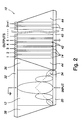
- Fig. 2 illustrates in greater detail the form of the IDTs 12 and 14 of the SAW device 10.
- the input AIDT 12 has a driven conductive rail 30 to which the input signal from the buffer 18 is applied, a grounded conductive rail 32, an apodization pattern having an axis, shown by a broken line 34, which has the shape of a V extending from the ends of the driven rail 30, and grounded front and rear tapered reflection suppressing dummy finger regions 36 and 38 respectively, all of the form known from Suthers et al. United States Patent No. 4,814,658 already referred to.
- the 2n+1 UIDTs 14 are all substantially identical to one another; they have a common grounded conductive rail 40, which is distinct from the grounded rail 32 to provide isolation between the input and output circuits of the SAW device, and respective output connections numbered 1 to 2n+1.
- the spacing of the IDTs 14 is such that a SAW propagated from the IDT 12 reaches successive output IDTs 14 after successive delays T, the delay period T being the reciprocal of the symbol rate.
- Grounded dummy fingers are provided in regions 42 between adjacent IDTs 14, and grounded tapered reflection suppressing regions 44 are provided adjacent the end IDTs 14 numbered 1 and 2n+1, the former region complementing the taper of the fingers 36 in the manner described in the Suthers et al. patent referred to above.
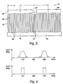
- Fig. 3 illustrates in greater detail the arrangement of two adjacent output IDTs 14, the output rails being referenced 46.
- each UIDT 14 is shown as extending over a distance of 3.5 wavelengths ⁇ at the IF, for which the SAW device 10 is designed, the fingers of each UIDT 14 having a pitch of ⁇ /2.
- the fingers are bifurcated to form pairs of inter-digital fingers 48 extending alternately from the grounded and output rails.
- each finger 48, and each gap between two adjacent fingers 48 has a width of ⁇ /8, the IDTs thereby having a metallization ratio of 0.5.
- Fig. 3 illustrates in greater detail the arrangement of two adjacent output IDTs 14, the output rails being referenced 46.
- each UIDT 14 is shown as extending over a distance of 3.5 wavelengths ⁇ at the IF, for which the SAW device 10 is designed, the fingers of each UIDT 14 having a pitch of ⁇ /2.
- the fingers are bifurcated to form pairs of inter-
- each UIDT 14 comprises 3 pairs of fingers 48 extending from the respective output rail 46 and 4 pairs of fingers extending from the grounded rail 40.
- the arrangement of the fingers of the AIDT 12 and of the grounded dummy fingers in the regions 36, 38, and 44 is similar, these fingers also being bifurcated with a finger pitch of ⁇ /2 (for each bifurcated finger pair) and also having a metallization ratio of 0.5.
- Fig. 3 also shows two grounded dummy fingers 50 in a region 42 between the two output IDTs 14. Because the symbol rate and the IF are independent and unrelated as already discussed above, the pitch or center-to-center spacing P of the UIDTs 14 is not an integral multiple of ⁇ /2, so that the grounded dummy fingers 50 in each region 42 between the IDTs 14 have a different width to that of the fingers 48 within the IDTs 14.
- the widths of the fingers 50 and the gaps therebetween are selected also to provide a metallization ratio of 0.5 to maintain a substantially constant SAW velocity. As can be seen in Fig. 3, in this case the fingers 50 and the associated gaps have slightly narrower widths than the fingers 48 and the gaps between them.
- the wavelength ⁇ is 1/140 MHz or 7.142857 ns.
- the pitch P of the UIDTs 14 is 1/35.84 MHz or 27.901785 ns, and the ratio of these is 3.90625.
- the pitch P corresponds to 3.90625 wavelengths ⁇ , of which 3.5 wavelengths are constituted by the finger pairs 48 of the output UIDTs 14 and the remaining 0.40625 wavelengths are taken up by the reduced-width dummy grounded fingers 50 and associated gaps.
- the reduced width of the fingers 50 in the regions 42 between the output IDTs 14 constitutes a discontinuity in the periodicity of fingers throughout the SAW device 10.
- This discontinuity is undesirable because it contributes to SAW reflections between the output IDTs, thereby detracting from the uniformity of the responses of the different output IDTs.
- the discontinuity can be avoided by constraining either the symbol rate of the system or the IF so that the IF is an integral multiple of half the symbol rate. However, this is also undesirable because it imposes a constraint upon either the symbol rate or the IF of the system.
- the present invention enables the IF and the symbol rate to be independent of one another, but avoids any discontinuity in the periodicity of fingers of the SAW device.
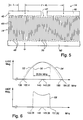
- Fig. 4 illustrates, at the top and bottom respectively, the frequency domain response magnitudes of a UIDT 14 and of an AIDT 12 of a SAW device 10 designed as described above to operate at a frequency of 140 MHz (the IF).
- This designed frequency is referred to below as the designed operating frequency of the SAW device 10, but it should be appreciated that the SAW device 10 actually has a bandpass filter characteristic with a pass band which, in the prior art, is centered on this designed operating frequency.
- the frequency domain response of an unapodized IDT such as the UIDTs 14 consists of a (sin x)/x function which is centered on the designed operating frequency of 140 MHz, the total response from 0 to twice this frequency, i.e. 280 MHz, being mirror imaged about the latter frequency so that a (sin x)/x function is also produced at the third harmonic of the operating frequency, i.e. centered on a frequency of 420 MHz.
- the frequency domain response of the apodized IDT which is determined by the apodization pattern of the AIDT, is designed to compensate for the (sin x)/x function, and also to give a desired overall frequency response for the IF signal in the microwave radio receiver.
- the apodization pattern of the AIDT 12 also serves as an IF spectral shaping filter.
- the frequency domain response of the AIDT 12 is thus designed to have a form such as that shown at the bottom of Fig. 4.
- This frequency response consists of pass bands centered at the operating frequency of 140 MHz and its third harmonic at 420 MHz, each extending, as is well known, by half the symbol rate of 35.84 MHz, i.e. by 17.92 MHz, above and below the center frequency.
- the attenuation of the AIDT in each pass band is complementary to the (sin x)/x function over the same frequency range.
- the desired frequency domain response of the AIDT 12 as shown at the bottom of Fig. 4 is used as an input to a Fast Fourier Transform (FFT) in order to synthesize the apodization pattern of the AIDT, i.e. to determine the finger lengths of the IDT throughout the apodization pattern.
- FFT Fast Fourier Transform
- using the frequency domain response directly would generally result in complex values for the length of each bifurcated finger pair.
- Each complex value can be considered to comprise a real value representing a finger length, which length is the same for the two fingers of a bifurcated finger pair, plus an imaginary value representing a phase shift or finger displacement in the direction of propagation of the SAW.
- Such finger displacement is undesirable and impractical to achieve with current photolithography techniques.
- the desired frequency domain response of the AIDT 12 is used to generate a Hermitian set of specifications, or Hermitian response, which when applied to the FFT to synthesize the AIDT apodization pattern results in real rather than complex values for the finger lengths or tap weights.
- the Hermitian response is such that the imaginary part of each result from the FFT is zero.
- a result of this process is that the individual fingers of each bifurcated finger pair, which would otherwise be of equal length, are now provided with individually determined and distinct lengths. (The use of the Hermitian response can be considered as transforming the finger displacement of two equal-length bifurcated fingers, as mentioned above, into unequal lengths of these fingers, without any finger displacement, to provide the same result.)
- the SAW device 10 is designed to have an operating frequency wavelength A which is determined in dependence upon the pitch or center-to-center spacing P of the consecutive output IDTs 14, so that the pitch P is an integral multiple of half the wavelength ⁇ .
- P k ⁇ /2, where k is an integer.
- this wavelength ⁇ is constant and determined for the entire SAW device 10, including the AIDT 12 and the grounded fingers in the regions 36, 38, and 44, as well as the UIDTs 14 and the grounded fingers in the regions 42.
- there is a constant periodicity of fingers i.e. the finger pitch of ⁇ /2 is constant), as well as a constant metallization ratio, throughout the entire SAW device 10, whereby SAW reflections between different parts of the device 10 are substantially eliminated.
- each UIDT 14 may be the same as the pitch P, so that the IDTs 14 are contiguous with one another and the regions 42 of grounded fingers 50 are dispensed with.
- the pitch P is 1/35.84 MHz or 27.901785 ns as before.
- the SAW device 10 is designed for an operating frequency wavelength of the symbol rate multiplied by k/2, i.e. 35.84 MHz multiplied by 4, or 143.36 MHz in this case.
- N is selected in this case to be equal to 3.5 (it must be an integral number of half-wavelengths) so that for each IDT 14 in Fig. 5, as in Fig. 3, there are three pairs of fingers 48 extending from each output rail 46, four associated pairs of fingers 48 extending from the grounded rail 40, and one pair of dummy grounded fingers 50 in each region 42 between adjacent output IDTs 14.
- Fig. 6 this illustrates, in a similar manner to Fig. 4 but on an expanded frequency scale in the region of the operating frequency, frequency domain responses for each UIDT 14 and for the AIDT 12.
- a dotted line curve 52 illustrates the response for each UIDT 14 in Fig. 4.
- this has a (sin x)/x shape centered on the operating frequency which is the IF of 140 MHz, and in accordance with the above equation has null frequencies at 100 and 180 MHz.
- a solid line curve 54 in the upper part of Fig. 6 each UIDT 14 in Fig.
- the UIDT response represented by the solid line curve 54 is asymmetric with respect to the IF.
- Fig. 6 illustrates by a curve 58 the complementary frequency domain response which the AIDT 12 is required to have in accordance with the invention.
- this has a pass band centered at the IF of 140 MHz and extending by half the symbol rate to the Nyquist frequencies above and below the IF, and within the pass band has an asymmetric attenuation which is complementary to the solid line curve 54 in the same frequency range.
- Fig. 7 illustrates, in a manner similar to that of Fig. 4, the frequency domain responses of each UIDT 14 and the AIDT 12 designed in accordance with the invention as described above with reference to Figs. 5 and 6, over the frequency range from 0 to 573.44 MHz (four times the designed operating frequency of 143.36 MHz).
- the UIDT response comprises a (sin x)/x function centered at the designed operating frequency of 143.36 MHz, the main central lobe of which corresponds to the solid line curve 54 in Fig. 6. This is mirror-imaged about twice the operating frequency, or 286.72 MHz, to produce a corresponding response centered at the third harmonic of 430.08 MHz.
- Fig. 7 shows the AIDT response curve 58 centered on the IF of 140 MHz, and hence offset from the center of the curve 54 so that it has the asymmetry as described above with reference to Fig. 6.
- the same design techniques are used as have already been described above.
- Hermitian specifications are created, in the known manner already referred to, to correspond to the response represented in the lower part of Fig. 7 and to result in real values when applied to an FFT to synthesize the AIDT apodization pattern.
- the FFT in this case has a maximum frequency of 573.44 MHz (i.e. 4 times 143.36 MHz, rather than 4 times 140 MHz as in the case of Figs. 3 and 4).
- the resulting real values determine the finger lengths or tap weights for the individual fingers of the bifurcated finger pairs of the AIDT 12.
- the SAW device 10 has a constant metallization ratio and a constant periodicity of fingers throughout its entire length, so that reflections and consequent impaired performance are avoided.
- the SAW device is designed so that its outputs at the IDTs 14 are successively delayed by the inverse of the symbol rate, as is desired for example for an ATDE, while the pass band of the SAW device is centered on a frequency which is independent of, and not integrally related to, the symbol rate, this frequency being the IF as described above. Accordingly, the SAW device eliminates any need for a predetermined relationship between the IF and the symbol rate.
- a pass band centered on the IF and with a bandwidth equal to the symbol rate (to provide a Nyquist filter) will initially be determined.
- a pass band centered on the IF and with a bandwidth equal to the symbol rate (to provide a Nyquist filter)
- the closest of these to the IF will be selected as the designed operating frequency of the SAW device.
- the wavelength ⁇ , and hence the finger pitch ⁇ /2, of the SAW device is thereby determined, and the remaining design follows the procedures described above.
- the output IDTs 14 have been described as being unapodized, and this would most conveniently be the case especially in view of the relatively small number of fingers in each IDT 14, this need not in fact be the case and an apodization pattern could be applied to the IDTs 14 (with all of these still being substantially identical to provide output signals which differ from one another only in their relative delays).
- the apodized IDT 12 has been referred to as an input IDT and the IDTs 14 have been referred to as output IDTs, and this would most conveniently be the case, the functions of these could be interchanged while still providing the advantages of the present invention.
- the SAW device 10 may take different forms from that specifically described above.
- the IDTs 14 may be distributed on both sides (front and rear) of the apodized IDT 12 instead of only on one side as illustrated in Fig. 2, thereby utilizing the SAWs propagated in opposite directions from the IDT 12.
- the IDTs 14 with odd-numbered outputs 1, 3,...2n+1 may be provided, with a pitch or center-to-center spacing of adjacent IDTs equal to twice the inverse of the symbol rate, and on the other side of the IDT 12 the IDTs 14 with even-numbered outputs 2, 4,...2n may be provided, also with a pitch or center-to-center spacing of adjacent IDTs equal to twice the inverse of the symbol rate.
Landscapes
- Physics & Mathematics (AREA)
- Acoustics & Sound (AREA)
- Surface Acoustic Wave Elements And Circuit Networks Thereof (AREA)
Abstract
Description
- This invention relates to SAW (surface acoustic wave) device tapped delay lines and to apparatus using such delay lines. Such apparatus may, for example, comprise an adaptive time delay equalizer of a receiver of a microwave radio digital signal communications system.
- It is well known to use SAW devices for filtering purposes. For example, Mitchell et al. United States Patent No. 3,968,461 issued July 6, 1976 and entitled "Acoustic Surface-Wave Devices" discloses a SAW device television intermediate frequency filter. This reference discusses Hermitian responses (symmetric amplitude and antisymmetric phase responses) of such filters, and describes a filter having an apodized interdigital transducer fingers of which are bifurcated, with the two halves of a finger having different lengths to provide the filter with a desired non-Hermitian response.
- SAW devices are also known to be used for filtering purposes in microwave radio communications systems. With increasing capacities of such systems, very stringent demands have been placed on the design and fabrication of such SAW devices, so that they have been developed to an advanced stage. For example, Suthers et al. United States Patent No. 4,814,658 issued March 21,1989 and entitled "SAW Device with Continuous Finger Pattern" describes and claims an advanced form of SAW device which is particularly useful for filtering purposes in microwave radio systems, and discusses earlier developments embodied in such a SAW device.
- In addition to filters, microwave radio systems include other circuits, such as equalizers, which can benefit by the incorporation therein of appropriate SAW devices. In particular, a microwave radio receiver invariably includes an ATDE (adaptive time domain equalizer), which may incorporate a transversal filter comprising a tapped delay line. In Birkett et al. United States Patent No. 5,051,709 issued September 24, 1991 and entitled "SAW Device Tapped Delay Line And Equalizer" there is described a SAW device tapped delay line which is particularly suitable for use at the IF (intermediate frequency) of a high capacity microwave radio communications system.
- A problem arises with such SAW device tapped delay lines in that the transmitted symbol rate of the system and the IF are independently determined. In particular, the IF is not an integral multiple of half the symbol rate. The symbol rate determines the pitch, or center-to-center spacing, of the IDTs (inter-digital transducers) which form the taps of the tapped delay line, whereas the pitch of the inter-digital fingers themselves is determined by the IF. Consequently, the IDT pitch is not an integral multiple of the finger pitch, so that there is necessarily a discontinuity in the finger pitch between adjacent IDTs. Such discontinuities give rise to reflections of a propagated SAW among the IDTs, with consequent deterioration in performance, and this is exacerbated by the large number (for example, 17) of IDT taps which may be necessary to achieve the required level of performance in a high capacity communications system.
- In the SAW device tapped delay line of Birkett et al., various arrangements of grounded dummy fingers are provided between adjacent IDT taps, but in each instance there is a discontinuity in periodicity due to the above consideration.
- There are various other arrangements of SAW device tapped delay line described in the prior art. However, again in each of these known arrangements there is a discontinuity in finger periodicity from each IDT tap to the next, usually no fingers at all being present in regions between the IDTs. As described above, these discontinuities give rise to impaired performance, which is sufficient largely to prevent SAW device tapped delay lines from being implemented in practical communications systems, in spite of the considerable advantages which they could otherwise provide.
- An object of this invention, therefore, is to provide an improved SAW device tapped delay line in which the problem described above is substantially eliminated.
- According to this invention there is provided a SAW (surface acoustic wave) device tapped delay line comprising: a first, apodized, IDT (inter-digital transducer) having a pass band centered at a first frequency; and a plurality of second IDTs, substantially identical to one another, arranged with a predetermined pitch P for consecutively receiving a SAW propagated from the first IDT with respective propagation delays; wherein each of the first and second IDTs comprises inter-digital fingers with a constant pitch, in the direction of SAW propagation, of λ/2 and P is an integral multiple of λ/2, where λ is the wavelength of a SAW at a second frequency within the pass band and different from the first frequency, and wherein the inter-digital fingers of the first IDT are bifurcated and weighted in accordance with a Hennitian response (symmetric amplitude and antisymmetric phase response) imaged about twice the second frequency.
- The SAW device preferably includes grounded dummy fingers in any regions between adjacent IDTs, all of the fingers of the IDTs and the dummy fingers being bifurcated and having said constant pitch whereby there is a constant finger periodicity throughout the SAW device. The second frequency is preferably an integral multiple of half the bandwidth of the pass band of the first IDT.
- The invention also extends to an ATDE (adaptive time delay equalizer) for operation at an IF (intermediate frequency) of a microwave radio communications system using QAM (quadrature-phase amplitude modulation) and communicating symbols at a predetermined symbol rate, comprising a SAW device tapped delay line as recited above wherein the first frequency is equal to the IF and the second frequency is an integral multiple of half the symbol rate.
- Thus the invention facilitates the provision of a SAW device tapped delay line, especially suitable for use in an ATDE of a high capacity microwave radio communications system, in which the pass band is centered on a first frequency (the IF) and the finger periodicity is dependent upon a second frequency, independent of the first frequency and within the pass band, which second frequency is made an integral multiple of half the symbol rate so that the finger periodicity can be constant throughout all of the SAW device.
- The invention will be further understood from the following description with reference to the accompanying drawings, in which similar references are used in different figures to denote similar components and in which:
- Fig. 1 is a block diagram illustrating an IF ATDE (intermediate frequency adaptive time delay equalizer), using a SAW (surface acoustic wave) device tapped delay line, for a microwave radio receiver;
- Fig. 2 illustrates the SAW device of Fig. 1 in greater detail;
- Fig. 3 illustrates in greater detail a previous arrangement of adjacent output IDTs (inter-digital transducers) of the SAW device of Fig. 2;
- Fig. 4 illustrates frequency domain responses of the unapodized and apodized IDTs of the SAW device of Figs. 2 and 3;
- Fig. 5 illustrates in greater detail an arrangement of adjacent output IDTs of the SAW device of Fig. 2 in accordance with this invention; and
- Figs. 6 and 7 illustrate frequency domain responses of the IDTs of the SAW device of Figs. 2 and 5 in accordance with this invention.
- Referring to Fig. 1, there is illustrated an ATDE for a QAM (quadrature-phase amplitude modulated) microwave radio receiver for equalizing I and Q carrier signal components, which are in phase quadrature, at an IF (intermediate frequency) of the receiver. Such an arrangement is described and claimed in United States Patent No. 5,051,709 already referred to.
- The ATDE of Fig. 1 comprises a transversal filter including a
SAW device 10 which provides a tapped delay line. TheSAW device 10 includes an apodized IDT (abbreviated below to AIDT) 12 and anumber 2n+1, where n is an integer, of unapodized IDTs (abbreviated below to UIDTs) 14 which serve as input and output IDTs respectively. An input IF signal is coupled to the input AIDT via abuffer 16 having a low output impedance, and optionally also via series tuning components which are not shown. The 2n+1 outputs from theUIDTs 14, each buffered by arespective buffer 18 having a low input impedance, are multiplied inmultipliers 20 by respective I component equalization coefficients I-n to I+n and Q component equalization coefficients Q-n to Q+n to produce currents throughresistors 22. These currents are summed insumming amplifiers quadrature hybrid 28 to produce an equalized IF output signal. The equalization coefficients are produced and automatically updated in known manner by control circuitry which is not shown. - Such an ATDE may be used for example in a 512-QAM digital microwave radio communications system in which each transmitted symbol represents 9 bits (2⁹=512), the transmitted symbol rate is 35.84 MHz (to be accommodated within a 40 MHz channel), and the IF is 140 MHz. The
SAW device 10 can have 17UIDTs 14, all substantially identical to one another, spaced apart from one another with a pitch (in the direction of propagation of a SAW from the input IDT 12) which corresponds to the symbol rate. It should be appreciated that in such a system the IF and symbol rate are independently determined, and there is not an integral multiple relationship between them. - Fig. 2 illustrates in greater detail the form of the
IDTs SAW device 10. The input AIDT 12 has a drivenconductive rail 30 to which the input signal from thebuffer 18 is applied, a groundedconductive rail 32, an apodization pattern having an axis, shown by abroken line 34, which has the shape of a V extending from the ends of the drivenrail 30, and grounded front and rear tapered reflection suppressingdummy finger regions UIDTs 14 are all substantially identical to one another; they have a common groundedconductive rail 40, which is distinct from the groundedrail 32 to provide isolation between the input and output circuits of the SAW device, and respective output connections numbered 1 to 2n+1. The spacing of theIDTs 14 is such that a SAW propagated from theIDT 12 reachessuccessive output IDTs 14 after successive delays T, the delay period T being the reciprocal of the symbol rate. Grounded dummy fingers are provided inregions 42 betweenadjacent IDTs 14, and grounded taperedreflection suppressing regions 44 are provided adjacent theend IDTs 14 numbered 1 and 2n+1, the former region complementing the taper of thefingers 36 in the manner described in the Suthers et al. patent referred to above. As a result of the presence of the grounded fingers in theregions SAW device 10 from the IDT 12 through all of theIDTs 14. - Fig. 3 illustrates in greater detail the arrangement of two
adjacent output IDTs 14, the output rails being referenced 46. In Fig. 3, eachUIDT 14 is shown as extending over a distance of 3.5 wavelengths λ at the IF, for which theSAW device 10 is designed, the fingers of eachUIDT 14 having a pitch of λ/2. In order to reduce reflections, as is well known the fingers are bifurcated to form pairs ofinter-digital fingers 48 extending alternately from the grounded and output rails. Within eachUIDT 14, eachfinger 48, and each gap between twoadjacent fingers 48, has a width of λ/8, the IDTs thereby having a metallization ratio of 0.5. Thus as shown in Fig. 3 eachUIDT 14 comprises 3 pairs offingers 48 extending from therespective output rail grounded rail 40. The arrangement of the fingers of the AIDT 12 and of the grounded dummy fingers in theregions - Fig. 3 also shows two grounded
dummy fingers 50 in aregion 42 between the twooutput IDTs 14. Because the symbol rate and the IF are independent and unrelated as already discussed above, the pitch or center-to-center spacing P of theUIDTs 14 is not an integral multiple of λ/2, so that the groundeddummy fingers 50 in eachregion 42 between theIDTs 14 have a different width to that of thefingers 48 within theIDTs 14. The widths of thefingers 50 and the gaps therebetween are selected also to provide a metallization ratio of 0.5 to maintain a substantially constant SAW velocity. As can be seen in Fig. 3, in this case thefingers 50 and the associated gaps have slightly narrower widths than thefingers 48 and the gaps between them. - More particularly, using the IF and symbol rate figures mentioned above, and representing distances in the SAW propagation direction by the times which it takes the SAW to propagate through such distances, the wavelength λ is 1/140 MHz or 7.142857 ns. The pitch P of the
UIDTs 14 is 1/35.84 MHz or 27.901785 ns, and the ratio of these is 3.90625. In other words, the pitch P corresponds to 3.90625 wavelengths λ, of which 3.5 wavelengths are constituted by the finger pairs 48 of the output UIDTs 14 and the remaining 0.40625 wavelengths are taken up by the reduced-width dummy groundedfingers 50 and associated gaps. - The reduced width of the
fingers 50 in theregions 42 between theoutput IDTs 14 constitutes a discontinuity in the periodicity of fingers throughout theSAW device 10. This discontinuity is undesirable because it contributes to SAW reflections between the output IDTs, thereby detracting from the uniformity of the responses of the different output IDTs. The discontinuity can be avoided by constraining either the symbol rate of the system or the IF so that the IF is an integral multiple of half the symbol rate. However, this is also undesirable because it imposes a constraint upon either the symbol rate or the IF of the system. The present invention enables the IF and the symbol rate to be independent of one another, but avoids any discontinuity in the periodicity of fingers of the SAW device. - Before describing the invention further, reference is made to Fig. 4 to provide an understanding of known design procedures for a SAW device such as the
device 10. Fig. 4 illustrates, at the top and bottom respectively, the frequency domain response magnitudes of aUIDT 14 and of anAIDT 12 of aSAW device 10 designed as described above to operate at a frequency of 140 MHz (the IF). This designed frequency is referred to below as the designed operating frequency of theSAW device 10, but it should be appreciated that theSAW device 10 actually has a bandpass filter characteristic with a pass band which, in the prior art, is centered on this designed operating frequency. - As illustrated at the top of Fig. 4, the frequency domain response of an unapodized IDT such as the
UIDTs 14 consists of a (sin x)/x function which is centered on the designed operating frequency of 140 MHz, the total response from 0 to twice this frequency, i.e. 280 MHz, being mirror imaged about the latter frequency so that a (sin x)/x function is also produced at the third harmonic of the operating frequency, i.e. centered on a frequency of 420 MHz. The frequency domain response of the apodized IDT, which is determined by the apodization pattern of the AIDT, is designed to compensate for the (sin x)/x function, and also to give a desired overall frequency response for the IF signal in the microwave radio receiver. In this respect, the apodization pattern of theAIDT 12 also serves as an IF spectral shaping filter. The frequency domain response of theAIDT 12 is thus designed to have a form such as that shown at the bottom of Fig. 4. This frequency response consists of pass bands centered at the operating frequency of 140 MHz and its third harmonic at 420 MHz, each extending, as is well known, by half the symbol rate of 35.84 MHz, i.e. by 17.92 MHz, above and below the center frequency. As is illustrated in Fig. 4, the attenuation of the AIDT in each pass band is complementary to the (sin x)/x function over the same frequency range. - The desired frequency domain response of the
AIDT 12 as shown at the bottom of Fig. 4 is used as an input to a Fast Fourier Transform (FFT) in order to synthesize the apodization pattern of the AIDT, i.e. to determine the finger lengths of the IDT throughout the apodization pattern. However, using the frequency domain response directly would generally result in complex values for the length of each bifurcated finger pair. (Each complex value can be considered to comprise a real value representing a finger length, which length is the same for the two fingers of a bifurcated finger pair, plus an imaginary value representing a phase shift or finger displacement in the direction of propagation of the SAW. However, such finger displacement is undesirable and impractical to achieve with current photolithography techniques.) - In order to avoid this problem, the desired frequency domain response of the
AIDT 12 is used to generate a Hermitian set of specifications, or Hermitian response, which when applied to the FFT to synthesize the AIDT apodization pattern results in real rather than complex values for the finger lengths or tap weights. In other words, the Hermitian response is such that the imaginary part of each result from the FFT is zero. A result of this process is that the individual fingers of each bifurcated finger pair, which would otherwise be of equal length, are now provided with individually determined and distinct lengths. (The use of the Hermitian response can be considered as transforming the finger displacement of two equal-length bifurcated fingers, as mentioned above, into unequal lengths of these fingers, without any finger displacement, to provide the same result.) - The use of a Hermitian response in this manner, together with the iterative use of a FFT to synthesize an AIDT, is known in the art. It is described, for example, in an article entitled "SAW Nyquist Filters For Digital Radio" by M. S. Suthers et al., IEEE 1987 Ultrasonics Symposium Proceedings, 1987, particularly in Sections 6.0 and 7.0 thereof. It is also described in greater detail in an article entitled "SAW Bandpass Filter Design Using Hermitian Function Techniques" by M. S. Suthers et al., IEEE Transactions on Sonics and Ultrasonics, Vol. SU-27, No. 2, March 1980.
- Referring now to Fig. 5, in accordance with this invention the
SAW device 10 is designed to have an operating frequency wavelength A which is determined in dependence upon the pitch or center-to-center spacing P of theconsecutive output IDTs 14, so that the pitch P is an integral multiple of half the wavelength λ. In other words, P = kλ/2, where k is an integer. It is important to appreciate that this wavelength λ is constant and determined for theentire SAW device 10, including theAIDT 12 and the grounded fingers in theregions UIDTs 14 and the grounded fingers in theregions 42. Thus there is a constant periodicity of fingers (i.e. the finger pitch of λ/2 is constant), as well as a constant metallization ratio, throughout theentire SAW device 10, whereby SAW reflections between different parts of thedevice 10 are substantially eliminated. - It should also be appreciated that in accordance with the invention the width of each UIDT 14 may be the same as the pitch P, so that the
IDTs 14 are contiguous with one another and theregions 42 of groundedfingers 50 are dispensed with. - Using the same figures as given above, in the
SAW device 10 whoseUIDTs 14 are as illustrated in Fig. 5 the pitch P is 1/35.84 MHz or 27.901785 ns as before. The designed operating frequency wavelength λ is determined in accordance with the equation P = kλ/2 so that the designed operating frequency is as close as possible to the IF of 140 MHz. This gives the result that k = 8 and P = 4λ as illustrated in Fig. 5. TheSAW device 10 is designed for an operating frequency wavelength of the symbol rate multiplied by k/2, i.e. 35.84 MHz multiplied by 4, or 143.36 MHz in this case. - As is well known, the bandwidth of each
output IDT 14 is determined by the total length N, in wavelengths λ at the operating frequency fo, of the IDT, in accordance with the equation fnull = (1 ± ¹/N) fo, where fnull gives the null frequencies on each side of the operating frequency. In view of the 40 MHz bandwidth already referred to, N is selected in this case to be equal to 3.5 (it must be an integral number of half-wavelengths) so that for eachIDT 14 in Fig. 5, as in Fig. 3, there are three pairs offingers 48 extending from eachoutput rail 46, four associated pairs offingers 48 extending from the groundedrail 40, and one pair of dummy groundedfingers 50 in eachregion 42 betweenadjacent output IDTs 14. - Referring to Fig. 6, this illustrates, in a similar manner to Fig. 4 but on an expanded frequency scale in the region of the operating frequency, frequency domain responses for each UIDT 14 and for the
AIDT 12. Initially referring only to the upper part of Fig. 6 showing the UIDT response, a dottedline curve 52 illustrates the response for each UIDT 14 in Fig. 4. As already described, this has a (sin x)/x shape centered on the operating frequency which is the IF of 140 MHz, and in accordance with the above equation has null frequencies at 100 and 180 MHz. In contrast, as shown by asolid line curve 54 in the upper part of Fig. 6, each UIDT 14 in Fig. 5 has its (sin x)/x shape centered on the operating frequency of 143.36 MHz determined as described above, so that as illustrated it has null frequencies at 102.4 and 184.32 MHz. As can be seen from the different heights at which dashedlines 56, representing the Nyquist frequencies (122.08 and 157.92 MHz) at half the symbol rate above and below the 140 MHz IF which the SAW device is intended to pass, the UIDT response represented by thesolid line curve 54 is asymmetric with respect to the IF. - The lower part of Fig. 6 illustrates by a
curve 58 the complementary frequency domain response which theAIDT 12 is required to have in accordance with the invention. As can be clearly seen from Fig. 6, this has a pass band centered at the IF of 140 MHz and extending by half the symbol rate to the Nyquist frequencies above and below the IF, and within the pass band has an asymmetric attenuation which is complementary to thesolid line curve 54 in the same frequency range. - Fig. 7 illustrates, in a manner similar to that of Fig. 4, the frequency domain responses of each UIDT 14 and the
AIDT 12 designed in accordance with the invention as described above with reference to Figs. 5 and 6, over the frequency range from 0 to 573.44 MHz (four times the designed operating frequency of 143.36 MHz). As illustrated in the upper part of Fig. 7, the UIDT response comprises a (sin x)/x function centered at the designed operating frequency of 143.36 MHz, the main central lobe of which corresponds to thesolid line curve 54 in Fig. 6. This is mirror-imaged about twice the operating frequency, or 286.72 MHz, to produce a corresponding response centered at the third harmonic of 430.08 MHz. - The lower part of Fig. 7 shows the
AIDT response curve 58 centered on the IF of 140 MHz, and hence offset from the center of thecurve 54 so that it has the asymmetry as described above with reference to Fig. 6. The imaged response is mirrored about twice the operating frequency, or 286.72 MHz, and hence is centered at a frequency of 286.72 x 2 - 140 = 433.44 MHz, so that it is also offset in frequency from the third harmonic response of the UIDT at 430.08 MHz, and is asymmetric as shown in Fig. 7. - In order to provide the
AIDT 12 with the response represented in the lower part of Fig. 7, the same design techniques are used as have already been described above. In other words Hermitian specifications are created, in the known manner already referred to, to correspond to the response represented in the lower part of Fig. 7 and to result in real values when applied to an FFT to synthesize the AIDT apodization pattern. The FFT in this case has a maximum frequency of 573.44 MHz (i.e. 4 times 143.36 MHz, rather than 4times 140 MHz as in the case of Figs. 3 and 4). The resulting real values determine the finger lengths or tap weights for the individual fingers of the bifurcated finger pairs of theAIDT 12. - The result of the above process in accordance with the invention is that the
SAW device 10 has a constant metallization ratio and a constant periodicity of fingers throughout its entire length, so that reflections and consequent impaired performance are avoided. At the same time, the SAW device is designed so that its outputs at theIDTs 14 are successively delayed by the inverse of the symbol rate, as is desired for example for an ATDE, while the pass band of the SAW device is centered on a frequency which is independent of, and not integrally related to, the symbol rate, this frequency being the IF as described above. Accordingly, the SAW device eliminates any need for a predetermined relationship between the IF and the symbol rate. - Although particular frequencies and time delays have been referred to above, it should be appreciated that the invention is not in any way limited by these, but that they are given by way of example to provide a full understanding of the invention. The same applies to the particular numbers of fingers used in each output IDT, the number of output IDTs, and other parameters.
- Thus considered more generally, for a SAW device tapped delay line to operate in an ATDE in a system with a given symbol rate and a given IF which are independent of one another, a pass band centered on the IF and with a bandwidth equal to the symbol rate (to provide a Nyquist filter) will initially be determined. Generally there will be two frequencies within this pass band which are integral multiples of half the symbol rate, and for ease of design the closest of these to the IF will be selected as the designed operating frequency of the SAW device. The wavelength λ, and hence the finger pitch λ/2, of the SAW device is thereby determined, and the remaining design follows the procedures described above.
- It should also be observed that, although for convenience the
output IDTs 14 have been described as being unapodized, and this would most conveniently be the case especially in view of the relatively small number of fingers in eachIDT 14, this need not in fact be the case and an apodization pattern could be applied to the IDTs 14 (with all of these still being substantially identical to provide output signals which differ from one another only in their relative delays). Furthermore, although the apodizedIDT 12 has been referred to as an input IDT and theIDTs 14 have been referred to as output IDTs, and this would most conveniently be the case, the functions of these could be interchanged while still providing the advantages of the present invention. - In addition, it should be appreciated that the
SAW device 10 may take different forms from that specifically described above. For example, in order to enable each of theIDTs 14 to extend over a greater number of wavelengths λ, to increase the number of groundedfingers 50 in each of theregions 42 between these IDTs 14, and/or to decrease insertion loss, theIDTs 14 may be distributed on both sides (front and rear) of the apodizedIDT 12 instead of only on one side as illustrated in Fig. 2, thereby utilizing the SAWs propagated in opposite directions from theIDT 12. Thus on one side of theIDT 12 theIDTs 14 with odd-numberedoutputs IDT 12 theIDTs 14 with even-numberedoutputs
Claims (5)
- A SAW (surface acoustic wave) device tapped delay line comprising:
a first, apodized, IDT (inter-digital transducer) (12) having a pass band (58) centered at a first frequency (140 MHz); and
a plurality of second IDTs (14), substantially identical to one another, arranged with a predetermined pitch P for consecutively receiving a SAW propagated from the first IDT with respective propagation delays;
wherein each of the first and second IDTs comprises inter-digital fingers (48) with a constant pitch, in the direction of SAW propagation, of λ/2 and P is an integral multiple of λ/2, when λ is the wavelength of a SAW at a second frequency (143.36 MHz) within the pass band and different from the first frequency, and wherein the inter-digital fingers of the first IDT are bifurcated and weighted in accordance with a Hermitian response imaged about twice the second frequency. - A SAW device tapped delay line as claimed in claim 1 wherein the fingers (48) of the second IDTs (14) are bifurcated.
- A SAW device tapped delay line as claimed in claim 1 and including grounded dummy fingers (42) in any regions between adjacent IDTs, all of the fingers (48) of the IDTs and the dummy fingers (42) being bifurcated and having said constant pitch whereby there is a constant finger periodicity throughout the SAW device.
- A SAW device tapped delay line as claimed in any of claims 1 to 3 wherein the second frequency (143.36 MHz) is an integral multiple of half the bandwidth (35.84 MHz) of the pass band of the first IDT (12).
- An ATDE (adaptive time delay equalizer) for operation at an IF (intermediate frequency) of a microwave radio communications system using QAM (quadrature-phase amplitude modulation) and communicating symbols at a predetermined symbol rate, comprising a SAW device tapped delay line as claimed in any of claims 1 to 3 wherein the first frequency is equal to the IF and the second frequency is an integral multiple of half the symbol rate.
Applications Claiming Priority (3)
| Application Number | Priority Date | Filing Date | Title |
|---|---|---|---|
| US07/639,606 US5122767A (en) | 1991-01-10 | 1991-01-10 | Saw device tapped delay lines |
| US639606 | 1991-01-10 | ||
| PCT/CA1991/000446 WO1992012573A1 (en) | 1991-01-10 | 1991-12-17 | Saw device tapped delay lines |
Publications (2)
| Publication Number | Publication Date |
|---|---|
| EP0566587A1 EP0566587A1 (en) | 1993-10-27 |
| EP0566587B1 true EP0566587B1 (en) | 1994-11-30 |
Family
ID=24564817
Family Applications (1)
| Application Number | Title | Priority Date | Filing Date |
|---|---|---|---|
| EP92900916A Expired - Lifetime EP0566587B1 (en) | 1991-01-10 | 1991-12-17 | Saw device tapped delay lines |
Country Status (6)
| Country | Link |
|---|---|
| US (1) | US5122767A (en) |
| EP (1) | EP0566587B1 (en) |
| JP (1) | JPH05509215A (en) |
| CA (1) | CA2096629C (en) |
| DE (1) | DE69105527T2 (en) |
| WO (1) | WO1992012573A1 (en) |
Families Citing this family (10)
| Publication number | Priority date | Publication date | Assignee | Title |
|---|---|---|---|---|
| FR2748872B1 (en) * | 1990-08-21 | 1998-11-27 | Thomson Trt Defense | MULTIPLE FRACTIONAL DIVISION PHASE LOCKED LOOP FREQUENCY SYNTHESIZER |
| JP4103666B2 (en) * | 2003-04-03 | 2008-06-18 | 株式会社村田製作所 | Wireless receiver |
| US20040239211A1 (en) * | 2003-06-02 | 2004-12-02 | Steve Beaudin | Surface wave device with weighted transducer |
| JP2006311353A (en) * | 2005-04-28 | 2006-11-09 | Samsung Electronics Co Ltd | Downconverter and upconverter |
| AU2009215118B2 (en) * | 2008-02-15 | 2015-01-22 | Tufts University | A humanized model of membrane attack complex (MAC) formation on murine retina and compositions, kits and methods for treatment of macular degeneration |
| US8877896B2 (en) | 2008-02-15 | 2014-11-04 | Tufts University | Compositions, methods and kits for modeling, diagnosing, and treating complement disorders |
| WO2012021891A2 (en) | 2010-08-13 | 2012-02-16 | Tufts University | Compositions, kits and methods for treatment of complement-related disorders |
| AU2015308773B2 (en) | 2014-08-28 | 2021-03-25 | Tufts University | Compositions, methods and kits for treating complement related disorders |
| KR20200119311A (en) | 2018-02-12 | 2020-10-19 | 트러스티즈 오브 터프츠 칼리지 | CD59 to inhibit inplasmasome activation |
| WO2023089564A1 (en) | 2021-11-19 | 2023-05-25 | Janssen Biotech, Inc. | Method of treating geographic atrophy with a gene therapy vector expressing soluble cd59 |
Family Cites Families (8)
| Publication number | Priority date | Publication date | Assignee | Title |
|---|---|---|---|---|
| GB1451326A (en) * | 1973-02-16 | 1976-09-29 | Nat Res Dev | Acoustic wave devices |
| GB1431112A (en) * | 1973-08-31 | 1976-04-07 | Mullard Ltd | Acoustic surface-wave devices |
| US4405874A (en) * | 1982-03-01 | 1983-09-20 | Northern Telecom Limited | Surface acoustic wave (saw) devices having series-connected inter-digital transducers |
| US4604595A (en) * | 1982-06-16 | 1986-08-05 | Murata Manufacturing Co., Ltd. | Surface acoustic wave device having interdigitated comb electrodes weighted for odd/even response |
| JPS598418A (en) * | 1982-07-06 | 1984-01-17 | Clarion Co Ltd | Surface acoustic wave device |
| JPH0773177B2 (en) * | 1984-12-17 | 1995-08-02 | 株式会社東芝 | Surface acoustic wave resonator |
| US4814658A (en) * | 1986-11-10 | 1989-03-21 | Northern Telecom Limited | SAW device with continuous finger pattern |
| CA1310079C (en) * | 1989-07-19 | 1992-11-10 | Alexander Neil Birkett | Saw device tapped delay line and apparatus using same |
-
1991
- 1991-01-10 US US07/639,606 patent/US5122767A/en not_active Expired - Lifetime
- 1991-12-17 WO PCT/CA1991/000446 patent/WO1992012573A1/en active IP Right Grant
- 1991-12-17 CA CA002096629A patent/CA2096629C/en not_active Expired - Fee Related
- 1991-12-17 DE DE69105527T patent/DE69105527T2/en not_active Expired - Fee Related
- 1991-12-17 JP JP4502019A patent/JPH05509215A/en active Pending
- 1991-12-17 EP EP92900916A patent/EP0566587B1/en not_active Expired - Lifetime
Non-Patent Citations (2)
| Title |
|---|
| IEEE 1987 ULTRASONICS SYMPOSIUM PROCEEDINGS vol. 1, 16 October 1987 New York, US pages 117-122; SUTHERS ET AL saw nyquist filters for digital radio cited in the application see page 118, left column, line 9 -right column, line 6 see page 118, right column, line 20 - page 120, right column, line 9; figures 4, 6, 11 * |
| TRANSACTIONS OF THE INSTITUTE OF ELECTRONICS AND COMMUNICATION vol. E62 no. 11, November 1979, TOKYO JP pages 775-778; TEMMYO et al. "A New Tapping Design for Low-Distortion SAW Tapped DElay Lines" see page 775, left column, line 13 - right column, line 4 see page 775, right column, line 23 - page 777, left column, line 34, see page 777, right column, line 8 - line 12; figure 1 * |
Also Published As
| Publication number | Publication date |
|---|---|
| CA2096629A1 (en) | 1992-07-11 |
| DE69105527T2 (en) | 1995-05-04 |
| DE69105527D1 (en) | 1995-01-12 |
| US5122767A (en) | 1992-06-16 |
| WO1992012573A1 (en) | 1992-07-23 |
| CA2096629C (en) | 1999-10-26 |
| EP0566587A1 (en) | 1993-10-27 |
| JPH05509215A (en) | 1993-12-16 |
Similar Documents
| Publication | Publication Date | Title |
|---|---|---|
| US6104260A (en) | Surface acoustic wave filter with first and second filter tracks and balanced or unbalanced terminals | |
| US6856214B2 (en) | Surface wave devices with low passband ripple | |
| US7532090B2 (en) | Acoustic wave filter device and duplexer | |
| US5486800A (en) | Surface acoustic wave device | |
| EP0566587B1 (en) | Saw device tapped delay lines | |
| US6462633B1 (en) | Surface acoustic wave device including parallel connected main and sub-filters | |
| EP0482033B1 (en) | Saw device tapped delay line and apparatus using same | |
| US5426339A (en) | Surface acoustic wave devices with mode changing characteristics | |
| US5670920A (en) | Multi-track SAW filter with reflectors and reversed polarity IDT connections | |
| US5300902A (en) | Surface acoustic wave device for band-pass filter having small insertion loss and predetermined pass-band characteristics for broad band | |
| EP0827274B1 (en) | Surface acoustic wave resonator filter | |
| JP4821079B2 (en) | Comb electrode section for surface acoustic wave, surface acoustic wave device, communication device | |
| EP0188604B1 (en) | Improved surface acoustic wave filter | |
| US4375624A (en) | Surface wave acoustic device with compensation for spurious frequency response modes | |
| KR100308867B1 (en) | Unidirectional surface acoustic wave transducer and transversal-type SAW filter having the same | |
| JP2004135259A (en) | Cascade-type surface acoustic wave filter system for eliminating temporal spurious response | |
| US20230130157A1 (en) | An alternative structure for realizing a transversal saw filter | |
| JP3196543B2 (en) | Surface wave filter | |
| Mishima et al. | IIDT type SAW filter using acoustic reflection cancel condition with solid IDT | |
| JP2003069371A (en) | Surface acoustic wave converter and saw filter employing the same | |
| JPH11243324A (en) | Surface acoustic wave transducer and surface acoustic wave filter |
Legal Events
| Date | Code | Title | Description |
|---|---|---|---|
| PUAI | Public reference made under article 153(3) epc to a published international application that has entered the european phase |
Free format text: ORIGINAL CODE: 0009012 |
|
| 17P | Request for examination filed |
Effective date: 19930610 |
|
| AK | Designated contracting states |
Kind code of ref document: A1 Designated state(s): DE FR GB |
|
| 17Q | First examination report despatched |
Effective date: 19940217 |
|
| GRAA | (expected) grant |
Free format text: ORIGINAL CODE: 0009210 |
|
| AK | Designated contracting states |
Kind code of ref document: B1 Designated state(s): DE FR GB |
|
| ET | Fr: translation filed | ||
| REF | Corresponds to: |
Ref document number: 69105527 Country of ref document: DE Date of ref document: 19950112 |
|
| PLBE | No opposition filed within time limit |
Free format text: ORIGINAL CODE: 0009261 |
|
| STAA | Information on the status of an ep patent application or granted ep patent |
Free format text: STATUS: NO OPPOSITION FILED WITHIN TIME LIMIT |
|
| 26N | No opposition filed | ||
| REG | Reference to a national code |
Ref country code: GB Ref legal event code: IF02 |
|
| REG | Reference to a national code |
Ref country code: FR Ref legal event code: CD |
|
| PGFP | Annual fee paid to national office [announced via postgrant information from national office to epo] |
Ref country code: GB Payment date: 20041119 Year of fee payment: 14 |
|
| PGFP | Annual fee paid to national office [announced via postgrant information from national office to epo] |
Ref country code: FR Payment date: 20041201 Year of fee payment: 14 |
|
| PGFP | Annual fee paid to national office [announced via postgrant information from national office to epo] |
Ref country code: DE Payment date: 20041230 Year of fee payment: 14 |
|
| PG25 | Lapsed in a contracting state [announced via postgrant information from national office to epo] |
Ref country code: GB Free format text: LAPSE BECAUSE OF NON-PAYMENT OF DUE FEES Effective date: 20051217 |
|
| PG25 | Lapsed in a contracting state [announced via postgrant information from national office to epo] |
Ref country code: DE Free format text: LAPSE BECAUSE OF NON-PAYMENT OF DUE FEES Effective date: 20060701 |
|
| GBPC | Gb: european patent ceased through non-payment of renewal fee |
Effective date: 20051217 |
|
| PG25 | Lapsed in a contracting state [announced via postgrant information from national office to epo] |
Ref country code: FR Free format text: LAPSE BECAUSE OF NON-PAYMENT OF DUE FEES Effective date: 20060831 |
|
| REG | Reference to a national code |
Ref country code: FR Ref legal event code: ST Effective date: 20060831 |