EP0565308B1 - Planar lens and low order array multiplexer - Google Patents
Planar lens and low order array multiplexer Download PDFInfo
- Publication number
- EP0565308B1 EP0565308B1 EP93302591A EP93302591A EP0565308B1 EP 0565308 B1 EP0565308 B1 EP 0565308B1 EP 93302591 A EP93302591 A EP 93302591A EP 93302591 A EP93302591 A EP 93302591A EP 0565308 B1 EP0565308 B1 EP 0565308B1
- Authority
- EP
- European Patent Office
- Prior art keywords
- waveguides
- input
- waveguide
- array
- output
- Prior art date
- Legal status (The legal status is an assumption and is not a legal conclusion. Google has not performed a legal analysis and makes no representation as to the accuracy of the status listed.)
- Expired - Lifetime
Links
Images


Classifications
-
- G—PHYSICS
- G02—OPTICS
- G02B—OPTICAL ELEMENTS, SYSTEMS OR APPARATUS
- G02B6/00—Light guides; Structural details of arrangements comprising light guides and other optical elements, e.g. couplings
- G02B6/10—Light guides; Structural details of arrangements comprising light guides and other optical elements, e.g. couplings of the optical waveguide type
- G02B6/12—Light guides; Structural details of arrangements comprising light guides and other optical elements, e.g. couplings of the optical waveguide type of the integrated circuit kind
- G02B6/12007—Light guides; Structural details of arrangements comprising light guides and other optical elements, e.g. couplings of the optical waveguide type of the integrated circuit kind forming wavelength selective elements, e.g. multiplexer, demultiplexer
- G02B6/12009—Light guides; Structural details of arrangements comprising light guides and other optical elements, e.g. couplings of the optical waveguide type of the integrated circuit kind forming wavelength selective elements, e.g. multiplexer, demultiplexer comprising arrayed waveguide grating [AWG] devices, i.e. with a phased array of waveguides
- G02B6/12011—Light guides; Structural details of arrangements comprising light guides and other optical elements, e.g. couplings of the optical waveguide type of the integrated circuit kind forming wavelength selective elements, e.g. multiplexer, demultiplexer comprising arrayed waveguide grating [AWG] devices, i.e. with a phased array of waveguides characterised by the arrayed waveguides, e.g. comprising a filled groove in the array section
-
- G—PHYSICS
- G02—OPTICS
- G02B—OPTICAL ELEMENTS, SYSTEMS OR APPARATUS
- G02B6/00—Light guides; Structural details of arrangements comprising light guides and other optical elements, e.g. couplings
- G02B6/10—Light guides; Structural details of arrangements comprising light guides and other optical elements, e.g. couplings of the optical waveguide type
- G02B6/12—Light guides; Structural details of arrangements comprising light guides and other optical elements, e.g. couplings of the optical waveguide type of the integrated circuit kind
- G02B6/122—Basic optical elements, e.g. light-guiding paths
- G02B6/124—Geodesic lenses or integrated gratings
- G02B6/1245—Geodesic lenses
-
- G—PHYSICS
- G02—OPTICS
- G02B—OPTICAL ELEMENTS, SYSTEMS OR APPARATUS
- G02B6/00—Light guides; Structural details of arrangements comprising light guides and other optical elements, e.g. couplings
- G02B6/24—Coupling light guides
- G02B6/26—Optical coupling means
- G02B6/28—Optical coupling means having data bus means, i.e. plural waveguides interconnected and providing an inherently bidirectional system by mixing and splitting signals
- G02B6/2804—Optical coupling means having data bus means, i.e. plural waveguides interconnected and providing an inherently bidirectional system by mixing and splitting signals forming multipart couplers without wavelength selective elements, e.g. "T" couplers, star couplers
Definitions
- This invention relates to an integrated optic device useful as a planar lens or a low order array multiplexer.
- the invention is particularly useful for broadband multiplexing or demultiplexing of optical signals.
- WDMs Broadband wavelength division multiplexers
- WDMs can be used to combine pump and signal wavelengths in an optical amplifying system.
- WDMs can be used to increase the long distance capacity of optical fibers by adding bands centered at different wavelengths. As an illustration, a band centered at 1.55 micrometers can be added to supplement capacity at the 1.30 micrometer band. The two bands can be used to provide bidirectional communications on a single fiber.
- WDMs require components capable of combining and separating optical signals in broad wavelength bands.
- Such components have been of primarily two types: Mach-Zehnder interferometers and wavelength dependent directional couplers.
- Mach-Zehnder interferometers and wavelength dependent directional couplers.
- Such devices are easily fabricated with optical waveguides using a single mask level, and they have low back reflection and high peak transmission. However, their spectral behavior is sinusoidal, and consequently they have low crosstalk over only a narrow wavelength range. Furthermore, it is very difficult to fabricate such devices with a precisely controlled wavelength of narrowband rejection. Consequently, interferometers and directional couplers are often inadequate for broadband applications, and thin film filters are needed to increase rejection ranges.
- FIG. 1 is a top view of a conventional waveguide array multiplexer 10 comprising a first array coupler 11 coupled via an array of n waveguides W 1 ,W 2 ,..., W n to a second array coupler 12.
- the array couplers 11 and 12 are typically slab waveguide regions each configured for providing substantially identical optical paths between an input or output point and a plurality of peripherally distributed waveguides.
- coupler 11 receives light at P i from an input waveguide 13, and coupler 12 distributes received light to a pair of output waveguides 14 and 15 near P o .
- the array of n waveguides between couplers 11 and 12 are arrayed in a "C" configuration with the waveguides spreading apart away from the couplers in order to reduce crosstalk.
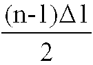
- Each successive waveguide provides an optical path which is longer than that of its predecessor by a constant amount ⁇ 1.
- An optical device useful as a planar lens or a low-order array multiplexer-demultiplexer comprises an input coupler, a plurality of closely spaced optical waveguides coupled by one of their ends to the output of the input coupler, at equal optical pathlengths from the input thereof, and an output coupler for receiving the other end of the plurality of closely spaced waveguides, wherein the waveguides are configured in an S-shaped array so as to present each a first region curved in a given direction and a second region curved in the opposite direction in a manner such that the total optical pathlength of the first and second curved regions is the same for each waveguide of the array.
- the second curved region of each waveguide of the array is directly connected to the first curved region thereof.
- each of the waveguides of the array comprises a third region between said first and second regions of opposite curvature, the third region presenting incrementally increasing lengths from one waveguide to the next.
- each successive waveguide has an increased length ⁇ 1 compared to its lower neighbor, and the waveguides terminate in a converging circle at coupler 12.
- ⁇ 1 m ⁇ o , where ⁇ 0 is the wavelength in the medium and m is an integer order number, then the phase front of the light in coupler 12 forms a circular wave converging on the coupler axis at P o .
- the phase front emerging from the array will be tilted at a small angle ⁇ relative to the coupler axis CC' and will couple efficiently near P 0 to waveguide 15 which is angularly displaced by ⁇ from the coupler axis.
- output waveguide 14 is positioned to couple to ⁇ o and output waveguide 15 to ⁇ 0 + ⁇ .
- This device can thus be used to receive a two wavelength input from waveguide 13 ( ⁇ o and ⁇ o + ⁇ ) and provide wavelength separated outputs, ⁇ o at 14 and ⁇ o + ⁇ at 15.
- the device thus acts as a grating and a demultiplexer. In the reverse direction it can act as a multiplexer.
- a difficulty with this conventional structure arises in efforts to make low order devices, i.e. devices with values of m less than about 10.
- Low order devices require path length differences ⁇ 1 on the order of a few wavelengths.
- the waveguides be separated for decoupling and that the waveguides avoid sharp bends to prevent loss.
- the "C" configuration array of FIG. 1 cannot be readily adapted to provide the small constant path length differences required for low order gratings.
- the conventional structure cannot be readily adapted for making broadband multiplexers or planar lenses.
- FIG. 2 is a schematic top view of a device adapted to operate as an integrated planar optic lens.
- the FIG. 2 device is similar to that of FIG. 1 except that the n waveguides (W 1 ,W 2 ,..., W n ) between array couplers 21 and 22 are arrayed in an "S" configuration rather than a "C” configuration.
- each waveguide comprises two substantially circular arcs which reverse direction of curvature at AA' half way between the couplers.
- each of the n waveguides presents the same length optical path between couplers 21 and 22.
- P i and P o are thus conjugate points, and the structure, with a single output waveguide 24, acts as a planar lens.
- coupler 21 is preferably a slab geometry waveguide in the configuration of a circular sector providing equal optical paths between an input waveguide 23 at P i and each of the plurality of circumferentially arrayed waveguides (W 1 , W 2 ,...,W n ).
- Coupler 22 is preferably a similar slab geometry waveguide receiving the plural waveguides at circumferential positions and providing equal paths from the guides to the center P o of 22.
- an "S" configuration integrated optic device can provide equal path lengths from P i to P o .
- each waveguide in the input section consists of straight segments connected with a circular arc having a radius of curvature equal to or larger than 15 mm.
- the input section waveguides have equal length differences between neighboring waveguides and are arranged in increasing length such that W 1 is the shortest and W n is the longest.
- the waveguides are also equally spaced at their intersection on line AA'.
- the output section is symmetrical with the direction of curvature reversed.
- ⁇ 0 was optimized at 30°.
- the total length and height of an exemplary device was 25 mm and 4 mm, respectively.
- the FIG. 2 device preferably comprises phosphorus doped glass waveguides on a silicon substrate advantageously fabricated as described in C. H. Henry, et al, "Glass Waveguides on Silicon for Hybrid Optical Packaging", 7 J . Lightwave Technol. , pp. 1530-1539 (1989).
- a silicon substrate is provided and a base layer of 15 micrometers of SiO 2 is grown on the silicon by high pressure steam oxidation.
- a core layer of 8% phosphorus doped glass having a thickness in the range of 3-4 micrometers is deposited on the oxide using LPCVD, and the core layer can be dry etched as by RIE to pattern the couplers and the waveguides.
- Typical waveguide core widths are in the range 4.5-6.5 micrometers, typical decoupling spacing between adjacent waveguides is thirty micrometers center-to-center, and typical minimum bending radius is about 15 mm.
- FIG. 3 is a schematic top view of a device in accordance with the invention adapted to act as a low order array demultiplexer.
- the "S" configuration grating is similar to the "S" configuration lens except that in the grating, substantially linear regions of incrementally increasing length are added to the waveguides in the region II of curve reversal. Specifically, the added segments 30 are the segments between AA' and BB'. With these added regions, each successive waveguide has a path length incrementally longer than its predecessor by an amount ⁇ 1. These increments are added without sharp bends or reduced spacing between waveguides. Thus successive waveguides in an "S" configuration grating can be readily provided with small incremental increases in length far smaller than the incremental increases in a "C" configuration device.
- the device can thus act as a demultiplexer like the device of FIG. 1, receiving channels of ⁇ 1 and ⁇ 2 on input waveguide 23 and providing separated output channels ⁇ 1 on output 24 and ⁇ 2 on 25.
- the device can act as a multiplexer presenting separate channels ⁇ 1 , ⁇ 2 at 24 and 25 to a single output guide 23.
- the mask layout for the FIG. 3 device is similar to that for the FIG. 2 device except for the extension section II located in the region of curve reversal between input section I and output section III.
- the waveguides in section II can conveniently be concentric arcs of small angle ⁇ w and radii of curvature equal to or greater than the minimum of 15 mm.
- FIGS. 4 and 5 are enlarged views of the regions near preferred couplers 21 and 22, respectively.
- a is the center-to-center spacing between waveguides W 1 , W 2 ,...,W n at the circumference of input coupler 21.
- the center of the circular wavefront is set back from the exit point of the waveguide by ⁇ Z.
- W is the waveguide width, and r is the array radius.
- ⁇ 1 and ⁇ 2 are the offset angles between the coupler axis CC' and the output waveguides 24 and 25 which receive wavebands centered at ⁇ 1 and ⁇ 2 respectively.
- ⁇ Za is the distance to the point at which the waveguides are directed for nearly symmetric array excitation.
- Table 1 Array 1 Array 2 Array 3 ⁇ 1 1.31 ⁇ m 1.475 ⁇ m 0.98 ⁇ m ⁇ 2 1.53 ⁇ m 1.55 ⁇ m 1.55 ⁇ m ⁇ 1 2.935 ⁇ m 8.356 ⁇ m 0.872 ⁇ m m(order) 3 8 1 a 9.0 ⁇ m 9.0 ⁇ m 9.0 ⁇ m w 5.5 ⁇ m 5.5 ⁇ m 4.5 ⁇ m ⁇ 1 -1.486° -1.340° -1.422° ⁇ 2 1.490° 1.341° 1.430° ⁇ Z 45 ⁇ m 45 ⁇ m 45 ⁇ m 45 ⁇ m ⁇ Za 220 ⁇ m 220 ⁇ m 220 ⁇ m r 590 mm 590 mm 600 mm
- the spectral transmission characteristics of the devices were then measured by coupling light through them using standard single mode fibers with a cutoff wavelength close to 1100 ⁇ m. Compared to conventional waveguide multiplexers, these devices exhibit wide spectral ranges of low crosstalk.
- the best performing device was array 1 whose measured transmission characteristics are plotted in FIG. 6.
- the crosstalk and fiber-to-fiber insertion loss for the device was about -35dB and -2dB, respectively, believed to be the lowest values yet reported for array multiplexers.
Landscapes
- Physics & Mathematics (AREA)
- General Physics & Mathematics (AREA)
- Optics & Photonics (AREA)
- Engineering & Computer Science (AREA)
- Microelectronics & Electronic Packaging (AREA)
- Optical Integrated Circuits (AREA)
- Optical Couplings Of Light Guides (AREA)
Description
- This invention relates to an integrated optic device useful as a planar lens or a low order array multiplexer. The invention is particularly useful for broadband multiplexing or demultiplexing of optical signals.
- Broadband wavelength division multiplexers (WDMs) have many applications in optical communications. For example, WDMs can be used to combine pump and signal wavelengths in an optical amplifying system. As another example, WDMs can be used to increase the long distance capacity of optical fibers by adding bands centered at different wavelengths. As an illustration, a band centered at 1.55 micrometers can be added to supplement capacity at the 1.30 micrometer band. The two bands can be used to provide bidirectional communications on a single fiber.
- WDMs require components capable of combining and separating optical signals in broad wavelength bands. Such components have been of primarily two types: Mach-Zehnder interferometers and wavelength dependent directional couplers. Such devices are easily fabricated with optical waveguides using a single mask level, and they have low back reflection and high peak transmission. However, their spectral behavior is sinusoidal, and consequently they have low crosstalk over only a narrow wavelength range. Furthermore, it is very difficult to fabricate such devices with a precisely controlled wavelength of narrowband rejection. Consequently, interferometers and directional couplers are often inadequate for broadband applications, and thin film filters are needed to increase rejection ranges.
- A new type of integrated optic multiplexer fabricated from waveguide arrays is described in US-A-5 002 350 or in EP-A-0 528652 (document under Art. 54(3) EPC). These integrated devices comprise an array of waveguides disposed between a pair of couplers. They are useful for making closely spaced, narrowband channels for dense wavelength division multiplexing. However, they are not suitable for broadband multiplexers requiring low order devices. Accordingly, there is a need for an integrated optic device which can be used as a low order grating or a lens.
- In the drawings:
- FIG. 1 is a schematic top view of a conventional integrated optic demultiplexer useful in illustrating the problems which the invention addresses;
- FIG. 2 is a schematic top view of an integrated planar optic lens in accordance with the invention;
- FIG. 3 is a schematic top view of an integrated low order grating in accordance with the invention;
- FIGS. 4 and 5 are schematic views of input and output array couplers, respectively, illustrating the structural parameters of the FIG. 3 device.
- FIG. 6 is a graphical illustration showing the performance characteristics of a device of the type shown in FIG. 3.
- Referring to the drawings, FIG. 1 is a top view of a conventional
waveguide array multiplexer 10 comprising afirst array coupler 11 coupled via an array of n waveguides W1 ,W2,..., Wn to asecond array coupler 12. Thearray couplers operation coupler 11 receives light at Pi from aninput waveguide 13, andcoupler 12 distributes received light to a pair ofoutput waveguides couplers - An optical device useful as a planar lens or a low-order array multiplexer-demultiplexer comprises an input coupler, a plurality of closely spaced optical waveguides coupled by one of their ends to the output of the input coupler, at equal optical pathlengths from the input thereof, and an output coupler for receiving the other end of the plurality of closely spaced waveguides, wherein the waveguides are configured in an S-shaped array so as to present each a first region curved in a given direction and a second region curved in the opposite direction in a manner such that the total optical pathlength of the first and second curved regions is the same for each waveguide of the array. For an optical lens the second curved region of each waveguide of the array is directly connected to the first curved region thereof. For a multiplexer-demultiplexer each of the waveguides of the array comprises a third region between said first and second regions of opposite curvature, the third region presenting incrementally increasing lengths from one waveguide to the next.
- In operation, light in the fundamental mode of
input waveguide 13 spreads by diffraction from the center ofcoupler 11, forming a circular wavefront of constant phase. The waveguides around the circumference ofcoupler 11 are all excited with the same phase. Since the waveguides separate, the optical signals become decoupled. However, after decoupling, the light in the waveguides initially continues with a circular phase front and retains nearly the same amplitude distribution as when the waveguides were initially excited. - The array is designed so that each successive waveguide has an increased length Δ1 compared to its lower neighbor, and the waveguides terminate in a converging circle at
coupler 12. If Δ1 = mλo, where λ0 is the wavelength in the medium and m is an integer order number, then the phase front of the light incoupler 12 forms a circular wave converging on the coupler axis at Po. At a different wavelength λo + Δλ, the phase front emerging from the array will be tilted at a small angle θ relative to the coupler axis CC' and will couple efficiently near P0 towaveguide 15 which is angularly displaced by θ from the coupler axis. In thisexample output waveguide 14 is positioned to couple to λo andoutput waveguide 15 to λ0+Δλ. This device can thus be used to receive a two wavelength input from waveguide 13 (λo andλo +Δλ) and provide wavelength separated outputs, λo at 14 and λo + Δλ at 15. The device thus acts as a grating and a demultiplexer. In the reverse direction it can act as a multiplexer. - A difficulty with this conventional structure arises in efforts to make low order devices, i.e. devices with values of m less than about 10. Low order devices require path length differences Δ1 on the order of a few wavelengths. There are also requirements that the waveguides be separated for decoupling and that the waveguides avoid sharp bends to prevent loss. In view of these competing requirements, the "C" configuration array of FIG. 1 cannot be readily adapted to provide the small constant path length differences required for low order gratings. Thus the conventional structure cannot be readily adapted for making broadband multiplexers or planar lenses.
- FIG. 2 is a schematic top view of a device adapted to operate as an integrated planar optic lens. The FIG. 2 device is similar to that of FIG. 1 except that the n waveguides (W 1,W 2,..., W n) between
array couplers couplers coupler 21 will arrive at the center Po ofcoupler 22 with the same phase from each of the n waveguides. Pi and Po are thus conjugate points, and the structure, with asingle output waveguide 24, acts as a planar lens. - Specifically,
coupler 21 is preferably a slab geometry waveguide in the configuration of a circular sector providing equal optical paths between aninput waveguide 23 at Pi and each of the plurality of circumferentially arrayed waveguides (W 1 , W 2,...,W n).Coupler 22 is preferably a similar slab geometry waveguide receiving the plural waveguides at circumferential positions and providing equal paths from the guides to the center Po of 22. - That the "S" configuration of waveguides can be designed to provide equal path lengths from 21 to 22 can be seen from FIG. 1 by considering a line of symmetry AA' perpendicular to the line Po Pi in the "C" configuration device. In the FIG. 1 device, the relationship between waveguide and pathlength is:

- As a guide to laying out the mask for the FIG. 2 structure, it can be seen from FIG. 2 that the straight waveguides forming the input coupler fanout are bent down to normal incidence on line AA', which is tilted by an angle of π/2 - γ0 relative to the input optical axis. Each waveguide in the input section consists of straight segments connected with a circular arc having a radius of curvature equal to or larger than 15 mm. The input section waveguides have equal length differences between neighboring waveguides and are arranged in increasing length such that W1 is the shortest and W n is the longest. The waveguides are also equally spaced at their intersection on line AA'. The output section is symmetrical with the direction of curvature reversed. In order to minimize the overall device dimension, γ0 was optimized at 30°. The total length and height of an exemplary device was 25 mm and 4 mm, respectively.
- The FIG. 2 device preferably comprises phosphorus doped glass waveguides on a silicon substrate advantageously fabricated as described in C. H. Henry, et al, "Glass Waveguides on Silicon for Hybrid Optical Packaging", 7 J. Lightwave Technol., pp. 1530-1539 (1989). In essence, a silicon substrate is provided and a base layer of 15 micrometers of SiO2 is grown on the silicon by high pressure steam oxidation. A core layer of 8% phosphorus doped glass having a thickness in the range of 3-4 micrometers is deposited on the oxide using LPCVD, and the core layer can be dry etched as by RIE to pattern the couplers and the waveguides. The core glass is then annealed, and thereafter a 7 micrometer layer of phosphorus and boron doped glass is deposited to act as a top cladding. Typical waveguide core widths are in the range 4.5-6.5 micrometers, typical decoupling spacing between adjacent waveguides is thirty micrometers center-to-center, and typical minimum bending radius is about 15 mm.
- FIG. 3 is a schematic top view of a device in accordance with the invention adapted to act as a low order array demultiplexer. The "S" configuration grating is similar to the "S" configuration lens except that in the grating, substantially linear regions of incrementally increasing length are added to the waveguides in the region II of curve reversal. Specifically, the added
segments 30 are the segments between AA' and BB'. With these added regions, each successive waveguide has a path length incrementally longer than its predecessor by an amount Δ1. These increments are added without sharp bends or reduced spacing between waveguides. Thus successive waveguides in an "S" configuration grating can be readily provided with small incremental increases in length far smaller than the incremental increases in a "C" configuration device. The device can thus act as a demultiplexer like the device of FIG. 1, receiving channels of λ1 and λ2 oninput waveguide 23 and providing separated output channels λ1 onoutput 24 and λ2 on 25. Alternatively, in the reverse direction, the device can act as a multiplexer presenting separate channels λ1, λ2 at 24 and 25 to asingle output guide 23. - The mask layout for the FIG. 3 device is similar to that for the FIG. 2 device except for the extension section II located in the region of curve reversal between input section I and output section III. The waveguides in section II can conveniently be concentric arcs of small angle θw and radii of curvature equal to or greater than the minimum of 15 mm. The path difference between the waveguides in section II -- which determines the total path length difference Δ1 -- is related to the angle θw and to the separation dh between waveguides along lines AA' and BB', by Δ1 = θwdh. By controlling θw, one can obtain array multiplexers of any desired order using the same design for sections I and III. In the limit of θw = 0, the device is a planar lens.
- "S" configuration arrays were fabricated in
orders preferred couplers input coupler 21. The center of the circular wavefront is set back from the exit point of the waveguide by ΔZ. W is the waveguide width, and r is the array radius. - As shown in FIG. 5, θ1 and θ2 are the offset angles between the coupler axis CC' and the
output waveguides - Applicants fabricated and tested three gratings (filters) having the parameters listed in Table 1 below:
Table 1 Array 1Array 2Array 3λ1 1.31 µm 1.475 µm 0.98 µm λ2 1.53 µm 1.55 µm 1.55 µm Δ1 2.935 µm 8.356 µm 0.872 µm m(order) 3 8 1 a 9.0 µm 9.0 µm 9.0 µm w 5.5 µm 5.5 µm 4.5 µm θ1 -1.486° -1.340° -1.422° θ2 1.490° 1.341° 1.430° ΔZ 45 µm 45 µm 45 µm ΔZa 220 µm 220 µm 220 µm r 590 mm 590 mm 600 mm - The spectral transmission characteristics of the devices were then measured by coupling light through them using standard single mode fibers with a cutoff wavelength close to 1100 µm. Compared to conventional waveguide multiplexers, these devices exhibit wide spectral ranges of low crosstalk. The best performing device was
array 1 whose measured transmission characteristics are plotted in FIG. 6. The crosstalk and fiber-to-fiber insertion loss for the device was about -35dB and -2dB, respectively, believed to be the lowest values yet reported for array multiplexers.
Claims (9)
- An optical device comprising an input coupler (21), a plurality of closely spaced optical waveguides (W1-Wn) coupled by one of their ends to the output of said input coupler, at equal optical pathlengths from the input thereof, and an output coupler (22) for receiving the other end of said plurality of closely spaced waveguides, CHARACTERISED IN THAT said waveguides are configured in an S-shaped array so as to present each a first region curved in a given direction and a second region curved in the opposite direction in a manner such that the total optical pathlength of said first and second curved regions is the same for each waveguide of the array.
- The device of claim 1, wherein said first and second curved regions have each a radius of curvature in excess of about 15 mm.
- The device of claim 1 or claim 2, wherein each waveguide in said array is normal to a line (A, A) tilted by an angle π/2-γ0 relative to the input optical axis (23).
- The device of claim 3, wherein γ0 is about 30°.
- The device of claim 3 or claim 4, wherein said waveguides are both normal to said line and equally spaced at said line.
- The device of any of the preceding claims, wherein said second curved region of each waveguide of the array is directly connected to said first curved region thereof so that all of said plurality of waveguides have equal optical pathlengths between said couplers, in order to act as a planar lens.
- The device of any of claims 1 to 5, wherein each of said waveguides of the array comprises a third region between said first and second regions of opposite curvature, wherein said third region presents an incrementally increasing length from one waveguide to the next so as to provide successive waveguides of said array with incrementally increasing optical pathlengths between said couplers, in order to act as a multiplexer or demultiplexer.
- The device of claim 7, wherein the input of said input coupler is provided with a single input waveguide (23) and the output of said output coupler is provided with plural output waveguides (24, 25) in order to act as a demultiplexer.
- The device of claim 7, wherein the input of said input coupler is provided with plural input waveguides and the output of said output coupler is provided with a single output waveguide in order to act as a multiplexer.
Applications Claiming Priority (2)
| Application Number | Priority Date | Filing Date | Title |
|---|---|---|---|
| US07/866,614 US5212758A (en) | 1992-04-10 | 1992-04-10 | Planar lens and low order array multiplexer |
| US866614 | 1992-04-10 |
Publications (2)
| Publication Number | Publication Date |
|---|---|
| EP0565308A1 EP0565308A1 (en) | 1993-10-13 |
| EP0565308B1 true EP0565308B1 (en) | 1997-07-23 |
Family
ID=25347994
Family Applications (1)
| Application Number | Title | Priority Date | Filing Date |
|---|---|---|---|
| EP93302591A Expired - Lifetime EP0565308B1 (en) | 1992-04-10 | 1993-04-01 | Planar lens and low order array multiplexer |
Country Status (4)
| Country | Link |
|---|---|
| US (1) | US5212758A (en) |
| EP (1) | EP0565308B1 (en) |
| JP (1) | JP2693354B2 (en) |
| DE (1) | DE69312369T2 (en) |
Families Citing this family (40)
| Publication number | Priority date | Publication date | Assignee | Title |
|---|---|---|---|---|
| JPH0310640A (en) * | 1989-06-09 | 1991-01-18 | Lotte Co Ltd | Fresh cream-containing chocolate and production thereof |
| US5425116A (en) * | 1993-11-16 | 1995-06-13 | At&T Corp. | Tunable optical waveguide grating arrangement |
| JP3425150B2 (en) * | 1994-02-11 | 2003-07-07 | コーニンクレッカ、フィリップス、エレクトロニクス、エヌ.ヴィ. | Optical device having a phase adjustment array |
| US5577141A (en) * | 1995-03-10 | 1996-11-19 | Lucent Technologies Inc. | Two-dimensional segmentation mode tapering for integrated optic waveguides |
| US5675675A (en) * | 1995-12-29 | 1997-10-07 | Corning Incorporated | Bandwidth-adjusted wavelength demultiplexer |
| JPH10509536A (en) * | 1995-09-20 | 1998-09-14 | フィリップス、エレクトロニクス、ネムローゼ、フェンノートシャップ | Optical integrated circuit including polarization converter |
| US5661825A (en) * | 1995-09-22 | 1997-08-26 | U.S. Philips Corporation | Integrated optical circuit comprising a polarization convertor |
| FR2743234B1 (en) | 1995-12-28 | 1998-01-23 | Alcatel Optronics | WAVELENGTH DEMULTIPLEXER |
| FR2743152B1 (en) * | 1995-12-28 | 1998-01-23 | Alcatel Optronics | OPTICAL DEMULTIPLEXER WITH GUIDE NETWORK |
| EP0786677B1 (en) * | 1996-01-25 | 2001-06-27 | Infineon Technologies AG | Method for operating a phased array |
| DE69723626T2 (en) * | 1996-08-06 | 2004-06-09 | Nippon Telegraph And Telephone Corp. | Waveguide array grating |
| DE69715043T2 (en) | 1996-12-23 | 2003-04-24 | Tellabs Denmark A/S, Ballerup | A BIDIRECTIONAL GUIDE AND A METHOD FOR UNIDIRECTIONAL REINFORCEMENT |
| JP2858655B2 (en) * | 1997-01-22 | 1999-02-17 | 日立電線株式会社 | Optical wavelength multiplexer / demultiplexer |
| EP0864891A1 (en) * | 1997-03-03 | 1998-09-16 | Akzo Nobel N.V. | Polymeric phased array |
| WO1998039676A1 (en) * | 1997-03-03 | 1998-09-11 | Akzo Nobel N.V. | Polymeric phased array |
| FR2772143B1 (en) * | 1997-12-08 | 2001-12-28 | France Telecom | OPTICAL COMPONENT WITH GUIDE NETWORK SPECTROGRAPH, WITH IMPROVED NETWORK GEOMETRY |
| FR2772144B1 (en) | 1997-12-08 | 2000-02-25 | France Telecom | OPTICAL SIGNAL EXCHANGE DEVICE THROUGH AN OPTICAL FIBER |
| FR2772145B1 (en) * | 1997-12-08 | 2003-06-27 | France Telecom | GUIDE NETWORK SPECTROGRAPH TYPE OPTICAL COMPONENT WITH CENTER OUTPUT CHANNELS |
| US6159526A (en) * | 1998-03-02 | 2000-12-12 | Fuji Oil Co., Ltd. | Method for manufacturing water-containing chocolates and chocolate compositions produced thereby |
| US6219471B1 (en) | 1999-01-15 | 2001-04-17 | Lucent Technologies Inc. | Optical device having equal length waveguide paths |
| US6947220B1 (en) | 1999-11-22 | 2005-09-20 | Ksm Associates, Inc. | Devices for information processing in optical communications |
| US6546161B2 (en) * | 2000-01-21 | 2003-04-08 | Nippon Telegraph And Telephone Corporation | No polarization dependent waveguide type optical circuit |
| US6529649B1 (en) * | 2000-05-01 | 2003-03-04 | Lucent Technologies Inc. | Optical filter with improved crosstalk rejection |
| US6473546B2 (en) * | 2000-07-28 | 2002-10-29 | Sumitomo Electric Industries, Ltd. | Optical multiplexer/demultiplexer |
| GB2366624A (en) * | 2000-09-01 | 2002-03-13 | Kymata Ltd | Optical arrayed waveguide grating |
| US6463197B1 (en) | 2000-11-01 | 2002-10-08 | Lucent Technologies Inc. | Coupling of optical signals to misaligned waveguides on different wafers |
| US6823096B2 (en) * | 2001-01-05 | 2004-11-23 | Lucent Technologies Inc. | Broadband optical switching arrangements with very low crosstalk |
| KR100401203B1 (en) * | 2001-11-13 | 2003-10-10 | 삼성전자주식회사 | Planar lightwave circuit with polynomial curve waveguide |
| GB2384320A (en) * | 2002-01-21 | 2003-07-23 | Bookham Technology Plc | Arrayed waveguide grating having opposing waveguide halves |
| WO2004083922A1 (en) * | 2003-03-21 | 2004-09-30 | Ignis Technologies As | Optical muliplexer based on arrayed waveguide grating |
| US8023822B2 (en) | 2005-02-10 | 2011-09-20 | Pirelli & C. S.P.A. | Optical band splitter/combiner device comprising a three-arms interferometer |
| JP4759423B2 (en) * | 2006-03-27 | 2011-08-31 | 富士通株式会社 | Optical transmission system |
| US7702200B2 (en) * | 2008-02-28 | 2010-04-20 | Corrado Pietro Dragone | Waveguide grating optical router suitable for CWDM |
| JP5644630B2 (en) * | 2011-03-30 | 2014-12-24 | 沖電気工業株式会社 | Optical waveguide device |
| US20150226367A1 (en) * | 2012-09-07 | 2015-08-13 | Creare Incorporated | Actuator for an in-line vacuum jacketed control valve for cryogenic fluids |
| JP6016312B2 (en) | 2012-09-14 | 2016-10-26 | 日本電信電話株式会社 | Optical multiplexer / demultiplexer |
| US10838146B2 (en) * | 2016-06-03 | 2020-11-17 | Rockley Photonics Limited | Single mode waveguide with an adiabatic bend |
| GB2572641B (en) | 2018-04-06 | 2021-06-02 | Rockley Photonics Ltd | Optoelectronic device and array thereof |
| WO2022184868A1 (en) | 2021-03-05 | 2022-09-09 | Rockley Photonics Limited | Waveguide facet interface |
| WO2022184869A1 (en) | 2021-03-05 | 2022-09-09 | Rockley Photonics Limited | Higher order mode filter |
Family Cites Families (10)
| Publication number | Priority date | Publication date | Assignee | Title |
|---|---|---|---|---|
| US3719462A (en) * | 1970-12-21 | 1973-03-06 | Bell Telephone Labor Inc | Light guide paths comprising densified regions in a transparent medium;and method of producing |
| US4763977A (en) * | 1985-01-09 | 1988-08-16 | Canadian Patents And Development Limited-Societe | Optical fiber coupler with tunable coupling ratio and method of making |
| JPH0718964B2 (en) * | 1987-06-29 | 1995-03-06 | 日本電信電話株式会社 | Integrated optical device and manufacturing method thereof |
| US4897671A (en) * | 1989-01-23 | 1990-01-30 | Polaroid Corporation | Integrated optic print head |
| DE3904752A1 (en) * | 1989-02-16 | 1990-08-23 | Siemens Ag | DEVICE FOR THE OPTICAL DIRECT RECEPTION OF SEVERAL WAVELENGTHS |
| US5117473A (en) * | 1989-08-08 | 1992-05-26 | E-Tek Dynamics, Inc. | Fiber optic coupler and method of making same |
| US5002350A (en) * | 1990-02-26 | 1991-03-26 | At&T Bell Laboratories | Optical multiplexer/demultiplexer |
| US5157746A (en) * | 1990-06-08 | 1992-10-20 | Brother Kogyo Kabushiki Kaisha | Optical waveguide array including two-dimensional lens and its manufacturing method |
| US5076654A (en) * | 1990-10-29 | 1991-12-31 | At&T Bell Laboratories | Packaging of silicon optical components |
| US5136671A (en) * | 1991-08-21 | 1992-08-04 | At&T Bell Laboratories | Optical switch, multiplexer, and demultiplexer |
-
1992
- 1992-04-10 US US07/866,614 patent/US5212758A/en not_active Expired - Lifetime
-
1993
- 1993-04-01 DE DE69312369T patent/DE69312369T2/en not_active Expired - Lifetime
- 1993-04-01 EP EP93302591A patent/EP0565308B1/en not_active Expired - Lifetime
- 1993-04-09 JP JP5106024A patent/JP2693354B2/en not_active Expired - Lifetime
Also Published As
| Publication number | Publication date |
|---|---|
| JP2693354B2 (en) | 1997-12-24 |
| EP0565308A1 (en) | 1993-10-13 |
| JPH0627339A (en) | 1994-02-04 |
| US5212758A (en) | 1993-05-18 |
| DE69312369T2 (en) | 1998-02-05 |
| DE69312369D1 (en) | 1997-08-28 |
Similar Documents
| Publication | Publication Date | Title |
|---|---|---|
| EP0565308B1 (en) | Planar lens and low order array multiplexer | |
| US5243672A (en) | Planar waveguide having optimized bend | |
| CA1265630A (en) | Multiplexer-demultiplexer using an elliptical concave garting and producted in integrated optics | |
| US6553165B1 (en) | Optical waveguide gratings | |
| US6768842B2 (en) | Arrayed waveguide grating | |
| EP0823647B1 (en) | Arrayed-waveguide grating | |
| US6434303B1 (en) | Optical waveguide slab structures | |
| US20020015559A1 (en) | Arrayed waveguide grating type optical multiplexer/demultiplexer and optical waveguide circuit | |
| US6501882B2 (en) | Arrayed waveguide grating type optical multiplexer/demultiplexer | |
| US6215924B1 (en) | Optical coupler device for dense wavelength division multiplexing | |
| US20020154861A1 (en) | Arrayed waveguide grating optical multiplexer/demultiplexer | |
| US7054526B2 (en) | Optical multiplexer/demultiplexer | |
| EP1113297A2 (en) | Arrayed waveguide grating multiplexer with tapered waveguides | |
| US6493487B1 (en) | Optical waveguide transmission devices | |
| US6665466B2 (en) | Optical multiplexer/demultiplexer | |
| US6591038B1 (en) | Optical interleaver and demultiplexing apparatus for wavelength division multiplexed optical communications | |
| US20030128927A1 (en) | Array waveguide grating | |
| EP1020740B1 (en) | Optical device having equal length waveguide paths | |
| US6714704B2 (en) | Optical component having selected bandwidth | |
| EP1430342B1 (en) | Passband flattening in an arrayed waveguide grating | |
| US6574397B2 (en) | Optical multiplexer/demultiplexer | |
| US6424760B1 (en) | Optical multiplexer/demultiplexer | |
| US6920265B2 (en) | Arrayed waveguide grating type optical multiplexer/demultiplexer | |
| US20030031412A1 (en) | Optical arrayed waveguide grating devices | |
| US6526202B1 (en) | Grating waveguide configuration for phasars |
Legal Events
| Date | Code | Title | Description |
|---|---|---|---|
| PUAI | Public reference made under article 153(3) epc to a published international application that has entered the european phase |
Free format text: ORIGINAL CODE: 0009012 |
|
| AK | Designated contracting states |
Kind code of ref document: A1 Designated state(s): DE FR GB |
|
| 17P | Request for examination filed |
Effective date: 19940331 |
|
| RAP3 | Party data changed (applicant data changed or rights of an application transferred) |
Owner name: AT&T CORP. |
|
| 17Q | First examination report despatched |
Effective date: 19960510 |
|
| GRAG | Despatch of communication of intention to grant |
Free format text: ORIGINAL CODE: EPIDOS AGRA |
|
| GRAH | Despatch of communication of intention to grant a patent |
Free format text: ORIGINAL CODE: EPIDOS IGRA |
|
| GRAH | Despatch of communication of intention to grant a patent |
Free format text: ORIGINAL CODE: EPIDOS IGRA |
|
| GRAA | (expected) grant |
Free format text: ORIGINAL CODE: 0009210 |
|
| AK | Designated contracting states |
Kind code of ref document: B1 Designated state(s): DE FR GB |
|
| REF | Corresponds to: |
Ref document number: 69312369 Country of ref document: DE Date of ref document: 19970828 |
|
| ET | Fr: translation filed | ||
| PLBE | No opposition filed within time limit |
Free format text: ORIGINAL CODE: 0009261 |
|
| STAA | Information on the status of an ep patent application or granted ep patent |
Free format text: STATUS: NO OPPOSITION FILED WITHIN TIME LIMIT |
|
| 26N | No opposition filed | ||
| REG | Reference to a national code |
Ref country code: GB Ref legal event code: IF02 |
|
| PGFP | Annual fee paid to national office [announced via postgrant information from national office to epo] |
Ref country code: DE Payment date: 20120411 Year of fee payment: 20 |
|
| PGFP | Annual fee paid to national office [announced via postgrant information from national office to epo] |
Ref country code: FR Payment date: 20120504 Year of fee payment: 20 Ref country code: GB Payment date: 20120404 Year of fee payment: 20 |
|
| REG | Reference to a national code |
Ref country code: DE Ref legal event code: R071 Ref document number: 69312369 Country of ref document: DE |
|
| REG | Reference to a national code |
Ref country code: GB Ref legal event code: PE20 Expiry date: 20130331 |
|
| PG25 | Lapsed in a contracting state [announced via postgrant information from national office to epo] |
Ref country code: GB Free format text: LAPSE BECAUSE OF EXPIRATION OF PROTECTION Effective date: 20130331 |
|
| PG25 | Lapsed in a contracting state [announced via postgrant information from national office to epo] |
Ref country code: DE Free format text: LAPSE BECAUSE OF EXPIRATION OF PROTECTION Effective date: 20130403 |