EP0565052A1 - Optical pick-up head apparatus wherein holographic optical element and photodetector are formed on semiconductor substrate - Google Patents
Optical pick-up head apparatus wherein holographic optical element and photodetector are formed on semiconductor substrate Download PDFInfo
- Publication number
- EP0565052A1 EP0565052A1 EP93105684A EP93105684A EP0565052A1 EP 0565052 A1 EP0565052 A1 EP 0565052A1 EP 93105684 A EP93105684 A EP 93105684A EP 93105684 A EP93105684 A EP 93105684A EP 0565052 A1 EP0565052 A1 EP 0565052A1
- Authority
- EP
- European Patent Office
- Prior art keywords
- photodetector
- optical element
- semiconductor substrate
- reflection type
- laser source
- Prior art date
- Legal status (The legal status is an assumption and is not a legal conclusion. Google has not performed a legal analysis and makes no representation as to the accuracy of the status listed.)
- Granted
Links
Images


Classifications
-
- G—PHYSICS
- G11—INFORMATION STORAGE
- G11B—INFORMATION STORAGE BASED ON RELATIVE MOVEMENT BETWEEN RECORD CARRIER AND TRANSDUCER
- G11B7/00—Recording or reproducing by optical means, e.g. recording using a thermal beam of optical radiation by modifying optical properties or the physical structure, reproducing using an optical beam at lower power by sensing optical properties; Record carriers therefor
- G11B7/12—Heads, e.g. forming of the optical beam spot or modulation of the optical beam
- G11B7/135—Means for guiding the beam from the source to the record carrier or from the record carrier to the detector
- G11B7/1353—Diffractive elements, e.g. holograms or gratings
-
- G—PHYSICS
- G11—INFORMATION STORAGE
- G11B—INFORMATION STORAGE BASED ON RELATIVE MOVEMENT BETWEEN RECORD CARRIER AND TRANSDUCER
- G11B7/00—Recording or reproducing by optical means, e.g. recording using a thermal beam of optical radiation by modifying optical properties or the physical structure, reproducing using an optical beam at lower power by sensing optical properties; Record carriers therefor
- G11B7/12—Heads, e.g. forming of the optical beam spot or modulation of the optical beam
- G11B7/123—Integrated head arrangements, e.g. with source and detectors mounted on the same substrate
Definitions
- the present invention relates to an optical pick-up head apparatus which can be used for recording and reproducing or erasing optical information on and from an optical storage medium such as an optical disc and an optical card.
- the optical memory technique utilizing a high-density and large-capacity storage medium such as an optical disc to record information by a pit-like pattern has been practiced as digital audio disc, video disc, document file disc and data file and has become widely applied to many fields.
- the reliability of the recording/reproduction of the optical information greatly depends upon the performance of an optical pick-up head apparatus used.
- the Japanese Utility Model Provisional Publication No. 58-162660 discloses a semiconductor apparatus in which a semiconductor laser, a reflector and a photodetector are formed in the same semiconductor substrate and the Japanese Patent Provisional Publication No.
- 2-52487 discloses an optical pick-up head apparatus in which a surface emitting laser is disposed on a photodetector.
- the Japanese Patent Provisional Publications Nos. 1-46243, 1-150244 and 2-253678 disclose optical pick-up head apparatus in which a photodetector and a reflector are formed in one semiconductor substrate and a semiconductor laser is disposed on the same semiconductor substrate.
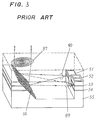
- Fig. 1 shows a conventional semiconductor apparatus as exemplified in the Japanese Utility Model Provisional Publication No. 58-162660.
- a semiconductor laser element 2 on a semiconductor substrate 1 there are formed a semiconductor laser element 2 and a reflection surface 3 whereby a laser beam emitted from the semiconductor laser 2 is reflected in a direction perpendicular to a surface of the semiconductor substrate 1 as indicated by an arrow A.
- a photodetector 4 is disposed on the surface of the semiconductor substrate 1 to receive an incident light beam as indicated by an arrow B.
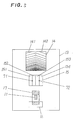
- Fig. 2 shows an optical pick-up head apparatus using as a light source the semiconductor apparatus as shown in Fig. 1, which apparatus is exemplified in the Japanese Patent Provisional Publication No. 64-27286.
- the laser beam A emitted from the semiconductor laser 2 and then reflected on the reflection surface 3 passes through a holographic optical element 5 and is converged by an objective lens 6 to be focused on an optical storage medium 7.
- the laser beam A is intensity-modulated in accordance with information recorded in the optical storage medium 7 and reflected therefrom.
- This reflected beam again passes through the objective lens 6 to be incident on the holographic optical element 5.
- this holographic optical element 5 has a function to generate a diffraction beam having an astigmatic aberration with respect to the reflected beam from the optical storage medium 7.
- This diffraction beam from the holographic optical element 5 is incident as the beam B on the photodetector 4.
- the photodetector 4 is divided into four areas which outputs electric signals in correspondence with the incident beams, respectively.
- the electric signals of the four-divided photodetector 4 are supplied to an adequate electric circuit to perform appropriate operations to provide a focusing error (FE) signal, a tracking error (TE) signal and an information (RF) signal corresponding to the information signal recorded on the optical storage medium 7.
- FE focusing error
- TE tracking error
- RF information
- Fig. 2 optical pick-up head apparatus since the semiconductor laser 2 and the photodetector 4 are formed on the same semiconductor substrate 1, the alignment therebetween can be made with an extremely high accuracy below 1 micron.
- the holographic optical element 5 is constructed as a different part spatially separated therefrom, and hence, in assembling the optical pick-up head apparatus, there is a problem that the holographic optical element 5 is required to be rotationally adjusted so that the beam from the holographic optical element 5 is incident on a desired position on the photodetector 4.
- an optical pick-up head apparatus comprising: a semiconductor laser source for emitting a coherent or semi-monochromatic beam; first reflection means for reflecting the beam from the semiconductor laser source to change the advancing direction of the beam therefrom; second reflection means for reflecting the beam reflected on the first reflection means to change the advancing direction thereof; third reflection means for reflecting the beam reflected on the second reflection means to change the advancing direction thereof; a converging optical system for receiving the beam reflected on the third reflection means to focus the beam on a microscopic spot on an optical storage medium; a reflection type holographic optical element for receiving the beam reflected and diffracted on the optical storage medium to generate a diffraction beam; and a photodetector having a plurality of photodetecting elements (light-receiving surfaces) to receive the diffraction beam from the reflection type holographic optical element to generate a photoelectric conversion signal, wherein the laser source is formed on a first semiconductor substrate so that the beam from the laser source is emitted in
- a diffraction grating is disposed in an optical path of the beam from the semiconductor laser source to the reflection type holographic optical element.
- an optical pick-up head apparatus comprising: a semiconductor laser source for emitting a coherent or semi-monochromatic beam; first reflection means for reflecting the beam from the semiconductor laser source to change the advancing direction of the beam therefrom; second reflection means for reflecting the beam reflected on the first reflection means to change the advancing direction thereof; third reflection means for reflecting the beam reflected on the second reflection means to change the advancing direction thereof; a converging optical system for receiving the beam reflected on the third reflection means to focus the beam on a microscopic spot on an optical storage medium; a reflection type holographic optical element for receiving the beam reflected and diffracted on the optical storage medium to generate a diffraction beam; and a photodetector having a plurality of photodetecting elements to receive the diffraction beam from the reflection type holographic optical element to generate a photoelectric conversion signal, wherein the laser source and the first reflection means are formed on a first semiconductor substrate, the beam from the laser source is emitted in a direction substantially parallel
- an optical pick-up head apparatus comprising: a semiconductor laser source for emitting a coherent or semi-monochromatic beam; first reflection means for reflecting the beam from the semiconductor laser source to change the advancing direction of the beam therefrom; second reflection means for reflecting the beam reflected on the first reflection means to change the advancing direction thereof; third reflection means for reflecting the beam reflected on the second reflection means to change the advancing direction thereof; a converging optical system for receiving the beam reflected on the third reflection means to focus the beam on a microscopic spot on an optical storage medium; a reflection type holographic optical element for receiving the beam reflected and diffracted on the optical storage medium to generate a diffraction beam; and a photodetector having a plurality of photodetecting elements to receive the diffraction beam from the reflection type holographic optical element to generate a photoelectric conversion signal, wherein the laser source, the first reflection means, the third reflection means and the photodetector are formed on one semiconductor substrate, the beam from the laser
- an optical pick-up head apparatus comprising: a semiconductor laser source for emitting a coherent or semi-monochromatic beam; first reflection means for reflecting the beam from the semiconductor laser source to change the advancing direction of the beam therefrom; second reflection means for reflecting the beam reflected on the first reflection means to change the advancing direction thereof; a converging optical system for receiving the beam reflected on the second reflection means to focus the beam on a microscopic spot on an optical storage medium; a reflection type holographic optical element for receiving the beam reflected and diffracted on the optical storage medium to generate a diffraction beam; and a photodetector having a plurality of photodetecting elements to receive the diffraction beam from the reflection type holographic optical element to generate a photoelectric conversion signal, wherein the reflection type holographic optical element is formed in the second reflection means, the diffraction beam from the reflection type holographic optical element is incident on the photodetector after being reflected on the first reflection means, the laser source is
- an optical pick-up head apparatus comprising: a semiconductor laser source for emitting a coherent or semi-monochromatic beam; first reflection means for reflecting the beam from the semiconductor laser source to change the advancing direction of the beam therefrom; second reflection means for reflecting the beam reflected on the first reflection means to change the advancing direction thereof; a converging optical system for receiving the beam reflected on the second reflection means to focus the beam on a microscopic spot on an optical storage medium; a reflection type holographic optical element for receiving the beam reflected and diffracted on the optical storage medium to generate a diffraction beam; and a photodetector having a plurality of photodetecting elements to receive the diffraction beam from the reflection type holographic optical element to generate a photoelectric conversion signal, wherein the reflection type holographic optical element is formed in the second reflection means, the diffraction beam from the reflection type holographic optical element is incident on the photodetector after being reflected on the first reflection means, the laser source,
- a reflection type diffraction grating is provided in the first or second reflection means and a second photodetector is disposed on the semiconductor substrate for receiving a portion of the beam from the semiconductor laser source which is not reflected and diffracted on the optical storage medium.
- the second photodetector is disposed to surround the reflection type holographic optical element.
- Fig. 4 A description will be made hereinbelow with reference to Fig. 4 in terms of an optical pick-up head apparatus according to a first embodiment of the present invention.
- This first semiconductor substrate 12 is mounted on a second semiconductor substrate 13.
- the first semiconductor substrate 12 is made of GaAs and the second semiconductor substrate is made of Si.
- Designated at numerals 15 and 16 are photodetectors formed on the second semiconductor substrate 13.
- the photodetector 15 is composed of a plurality of photodetecting elements (light-receiving surfaces) and the photodetector 16 is composed of one photodetecting element.
- first and third reflecting portions 17 and 14 are formed on the second semiconductor substrate 13 .
- the third reflecting portion 14 acts as a reflection type holographic optical element.
- the reflection type holographic optical element 14 is blazed in order to suppress generation of unnecessary diffraction beams causing noises.
- the semiconductor laser source 11 generates a laser beam toward the first reflector 17 in a direction parallel to the surface of the first semiconductor substrate 12.
- the beam 70 advances toward a second reflector 18 to be reflected thereon.
- the reflected beam from the second reflector 18 advances to be incident on the reflection type holographic optical element 14 formed on the second semiconductor substrate 13.
- the reflected beam on the reflection type holographic optical element 14 passes through an objective lens 19 so as to be converged to be focused on an optical storage medium 20 comprising a transparent substrate 21 having grooves or pits and a protective film 20 covering the transparent substrate 21.
- the reflection type holographic optical element 14 is blazed as described above, it is possible to prevent a diffraction beam generated due to the holographic optical element 14 from being incident as noises on the photodetector 15.
- the beam reflected and diffracted on the optical storage medium 20 advances along the return path, that is, the reflected and diffracted beam thereon is incident on the reflection type holographic optical element 14 after passing through the objective lens 19.
- the incident beam on the reflection type holographic optical element 14 is reflected whereby a plurality of diffraction beams generate.
- the zero order diffraction beam from the reflection type holographic optical element 14 advances along the same path in the opposite direction to be incident on the semiconductor laser source 11, that is, returns to the semiconductor laser source 11 after reflections on the second reflector 18 and the first reflector 17.
- the first order diffraction beams 71 and 72 from the reflection type holographic optical element 14 are incident on the photodetector 15 after being reflected on the second reflector 18.
- the relation between the hologram pattern recorded in the reflection type holographic optical element 14 and the first order diffraction beams 71, 72 and the methods to detecting the FE signal, TE signal and RF signal will hereinafter be described in detail
- the semiconductor laser source 11 also generates a laser beam 700 from its other end (rear end) toward the photodetector 16. This laser beam 700 is incident on the photodetector 16 to be converted into an electric signal which is in turn used as a reference signal for a control circuit, not shown, to keep the output of the semiconductor laser source 11 constant.
- the photodetector 15 and the reflection type holographic optical element 14 are formed on the same semiconductor substrate.
- the relative positional relation therebetween can be determined at a high accuracy below about 1 micron.
- the semiconductor laser source 11 is disposed at a position extremely close spatially to the second semiconductor substrate 13, as compared with the case that the semiconductor laser source 11 is spatially separated therefrom, it is possible to heighten the positional accuracy of the semiconductor laser source 11.
- the semiconductor laser source 11 if alignment marks are formed on the semiconductor substrate 13 and the semiconductor laser source 11, it is possible to mount the semiconductor laser source 11 on a desired position of the semiconductor substrate 13 with a high accuracy (for example, accuracy of several ⁇ m). As a result, it is possible to take the relative positional relation between the photodetector 15 and the semiconductor laser source 11 with a high accuracy. That is, the semiconductor laser source 11, reflection type holographic optical element 14 and the photodetector 15 can stably be arranged with a high accuracy.
- the semiconductor laser source 11, reflection type holographic optical element 14 and the photodetector 15 can stably be arranged with a high accuracy and the semiconductor laser source 11 and the photodetector 15 take a substantial conjugate relation to each other, the first order diffraction beams 71 and 72 to be incident on the photodetector 15 scarcely varies, thereby preventing the deterioration of the FE signal, TE signal and RF signal to be detected.
- this embodiment can increase the mass productivity of the optical pick-up head apparatus and decrease the assembling cost thereof.
- Fig. 5 is a top view of the second semiconductor substrate 13.
- the reflection type holographic optical element 14 has two hologram areas 141 and 142 which produce the first order diffraction beams 71 and 72, respectively.
- the photodetector 15 has four photodetecting elements 151, 152, 153 and 154.
- the first order diffraction beam 71 from the reflection type holographic optical element 14 is received by the photodetecting elements 151 and 152 and the first order diffraction beam 72 therefrom is received by the photodetecting elements 153 and 154.
- Each of the hologram areas 141 and 142 can be realized with the semiconductor laser source 11 and the converged point of the beam received at a desired position on the photodetector 15 being taken as virtual light sources and an interference pattern made on the reflection type holographic optical element 14 by the beams emitted from these light sources being calculated and recorded on the hologram area.
- the patterns of the reflection type hologram areas 141 and 142 is formed on a photomask and the reflection type holographic optical element 14 is formed on the semiconductor substrate 13 using the photomask and techniques such as exposure and etching generally taken in the semiconductor apparatus manufacturing process.
- the reflector 17 can be formed on the semiconductor substrate 13 in accordance with such techniques.
- a large number of semiconductor substrate 13 each having the reflection type holographic optical element 14 can be manufactured from one semiconductor substrate wafer.
- Figs. 6A to 6C show the first order diffraction beams 71 and 72 relative to the respective photodetecting elements 151 to 154 of the photodetector 15 in the optical pick-up head apparatus illustrated in Fig. 4.
- Fig. 6B shows the case that the beam 70 emitted from the semiconductor laser source 11 is focused on the optical storage medium 20, and
- Figs. 6A and 6C respectively show the cases that the beam 70 therefrom takes defocusing states with respect to the optical storage medium 20.
- the FE signal can be obtained by performing the differential operation between the sum of the outputs of the photodetecting elements 151 and 154 and the sum of the outputs of the photodetecting elements 152 and 153.
- This FE signal detecting method is so-called double knife edge method. After necessary processes such as amplification, phase-compensation and band-limitation, the FE signal is supplied to a focusing control actuator 91 shown in Fig. 4 whereby the position of the objective lens 19 in the focusing direction is controlled so that the focal point of the objective lens 19 is at a desired position on the optical storage medium 20.
- the TE signal can be obtained by performing the differential operation between the sum of the outputs of the photodetecting elements 151, 152 and the sum of the outputs of the photodetecting elements 153, 154 under the condition that the relation between farfield patterns of the first order diffraction beams 71, 72 and the photodetecting elements 151 to 154 is taken as illustrated in Fig.
- This TE signal detecting method is so-called push-pull method.
- the TE signal is supplied to a tracking control actuator 92 as illustrated in Fig. 4 whereby the position of the objective lens 19 in the radial direction of the optical storage medium 20 is controlled so that the focal point of the objective lens 19 is at a desired position such as a pit, track and land of the optical storage medium 20.
- the RF signal can be obtained on the basis of the total sum of the outputs of the photodetecting elements 151 to 154.
- the RF signal is led to a signal processing circuit, not shown, to reproduce the information recorded in the optical storage medium 20.
- An optical pick-up head apparatus using the double edge method and push-pull method to obtain the FE signal and the TE signal is known as exemplified in US Patent 4665310.
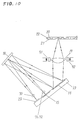
- numeral 51 designates a semiconductor laser source
- 52 represents a photodetector
- 53, 54 denote active layers
- 55 depicts a semiconductor substrate
- 56 indicates a reflection type holographic optical element
- 57 is a Fresnel's collimating lens.
- a beam 90 emitted from the semiconductor laser source 51 is reflected and diffracted on an optical storage medium and then incident on the reflection type holographic optical element 56 so as to produce a diffraction beam 89 which is in turn incident on the photodetector 52.
- Fig. 1 designates a semiconductor laser source
- 52 represents a photodetector
- 53, 54 denote active layers
- 55 depicts a semiconductor substrate
- 56 indicates a reflection type holographic optical element
- 57 is a Fresnel's collimating lens.
- a beam 90 emitted from the semiconductor laser source 51 is reflected and diffracted on an optical storage medium and then incident on the reflection type holographic optical element 56 so as to produce
- the diffraction beam 89 from the reflection type holographic optical element 56 is directly received by the photodetector 52.
- the light-receiving portion of the photodetector 52 is required to be formed in a plane perpendicular to the semiconductor substrate 55 disposed between the active layers 54 and 53. This region is required to be formed through the crystal growth.
- the width of the light-receiving portion is required to be about 10 to 100 microns and hence a very long time is required for the crystal growth.
- the photodetector 15 can be formed for a short time period without the crystal growth.
- the semiconductor laser source 51 is arranged to be close to the reflection type holographic optical element 56, the pattern of the reflection type holographic optical element 56 becomes very fine or minute, whereby difficulty is encountered to form the pattern of the reflection type holographic optical element 56.
- the distance between the semiconductor laser source 51 and the reflection type holographic optical element 56 is preferable to be above 1 mm in practice.
- the reflection type holographic optical element 56 is formed in a plane inclined with respect to the surface of the semiconductor substrate 55, as the reflection type holographic optical element 56 is separated from the semiconductor laser source 51, the thickness of the semiconductor substrate 55 is required to be increased. In addition, the time necessary for the etching to form the reflection type holographic optical element 56 becomes long.
- the reflection type holographic optical element 14 is formed in a plane parallel to the surface of the semiconductor substrate 13 and disposed at a position sufficiently separated from the semiconductor laser light source 11, and hence it is possible to prevent the pattern of the reflection type holographic optical element 14 from becoming fine and further prevent the time necessary for the etching from becoming long in manufacturing.
- the reflector 17 is also formed by the etching of the semiconductor substrate 13, any pattern is not formed in the reflector 17 and therefore the reflector 17 can be disposed at a position close to the semiconductor laser light source 11. Thus, it is possible to reduce the thickness of the semiconductor substrate 13 to shorten the time necessary for the etching.
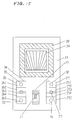
- FIG. 7 shows an optical pick-up head apparatus according to the second embodiment of this invention where parts corresponding to those in Fig. 4 are marked with the same numerals and the description thereof will be omitted for brevity.
- the first reflector 17, photodetector 15 and reflection type holographic optical element 14 are formed on the same semiconductor substrate 13 and the semiconductor laser source 11 is formed on the semiconductor substrate 12, in this embodiment the semiconductor laser source 11 and the first reflector 17 are formed on the semiconductor substrate 12 and the photodetector 15 and the reflection type holographic optical element 14 are formed on the semiconductor substrate 13.
- the beam 70 emitted from the semiconductor laser source 11 is successively reflected on the reflectors 17, 18 and the reflection type holographic optical element 14 and then focused on the optical storage medium 20 through the objective lens 19.
- the beam 70 reflected and diffracted on the optical storage medium 20 is incident on the reflection type holographic optical element 14 to become the first order diffraction beams 71 and 72.
- the first order diffraction beams 71 and 72 are reflected on the reflector 18 and then incident on the photodetector 15.
- the relative positional relation between the photodetector 15 and the reflection type holographic optical element 14 can be determined at a high accuracy below about 1 micron, thereby not requiring the positional or rotational adjustment of the reflection type holographic optical element 14 or the photodetector 15 in assembling the optical pick-up head apparatus.
- the semiconductor laser source 11 is mounted on the semiconductor substrate 13, i.e., disposed at a position extremely close spatially to the semiconductor substrate 13, the positional accuracy of the semiconductor laser source 11 becomes high.
- the semiconductor laser source 11, reflection type holographic optical element 14 and photodetector 15 can stably be arranged with a high accuracy and the semiconductor laser source 11 and photodetector 15 take a substantial conjugate relation to each other, the first order diffraction beams 71 and 72 to be received by the photodetector 15 scarcely vary, thereby preventing the deterioration of the FE, TE and RF signals. That is, because of scarcely requiring the adjustment in assembling, the mass productivity can be increased to reduce the assembling cost of the optical pick-up head apparatus.
- Fig. 8 shows an optical pick-up head apparatus according to the third embodiment of this invention where parts corresponding to those in Fig. 4 or 7 are marked with the same numerals and the description thereof will be omitted for brevity.
- the relative positional relation between the semiconductor laser source 11, photodetector 15 and the reflection type holographic optical element 14 can be determined with a high accuracy below about 1 micron, thereby not requiring the positional or rotational adjustment of the reflection type holographic optical element 14 or the photodetector 15 in assembling the optical pick-up head apparatus.
- the semiconductor laser source 11 is required to be mounted on the semiconductor substrate 13, this embodiment does not require such a mounting work, thereby improving the mass productivity.
- FIG. 9 shows an optical pick-up head apparatus according to the fourth embodiment of this invention where parts corresponding to those in Fig. 4, 7 or 8 are marked with the same numerals and the description thereof will be omitted for brevity.
- the first reflector 17, photodetector 15 and the reflection type holographic optical element 14 are formed on the same semiconductor substrate 13 and the semiconductor laser source 11 is formed on the semiconductor substrate 12, in this embodiment the photodetector 15 and reflection type holographic optical element 14 are formed on the semiconductor substrate 13 and a surface emitting laser source 23 is used in place of the semiconductor laser source 11. This arrangement does not require the first reflector 17.
- the surface emitting laser source 23 is formed on the semiconductor substrate 12 and then mounted on the semiconductor substrate 13.
- the beam 70 emitted from the surface emitting laser source 23 is reflected on the reflector 18 and further reflected on the reflection type holographic optical element 14 and then focused on the optical storage medium 20 through the objective lens 19.
- the beam 70 reflected and diffracted on the optical storage medium 20 is incident on the reflection type holographic optical element 14 so as to become the diffraction beams 71 and 72 which are in turn reflected on the reflector 18 to be incident on the photodetector 15.
- the relative positional relation therebetween can be determined with a high accuracy below about 1 micron, thereby not requiring the positional or rotational adjustment of the reflection type holographic optical element 14 and the photodetector 15 in assembling the optical pick-up head apparatus.
- the optical pick-up head apparatus which is capable of stably obtaining the signals irrespective of no adjustment.
- the beam 70 emitted from the semiconductor laser source 11 are reflected on three portions of the reflectors 17, 18 and the reflection type holographic optical element 14
- the beam 70 emitted from the surface emitting laser source 23 is reflected on the two portions of the reflector 18 and the reflection type holographic optical element 14.
- Fig. 10 shows an optical pick-up head apparatus according to the fifth embodiment where parts corresponding to those in Fig. 9 are marked with the same numerals.
- the photodetector 15 and reflection type holographic optical element 14 are formed on the same semiconductor substrate 13 and the surface emitting laser source 23 is formed on the semiconductor substrate 12, in this embodiment the surface emitting laser 23, photodetector 15 and reflection type holographic optical element 14 are formed on the same semiconductor substrate 13.
- the beam 70 emitted from the surface emitting laser source 23 is reflected on the reflector 18 and the reflection type holographic optical element 14 and then focused on the optical storage medium 20 through the objective lens 19.
- the beam 70 reflected and diffracted on the optical storage medium 20 is incident on the reflection type holographic optical element 14 to become the first order diffraction beams 71 and 72 which are in turn incident on the photodetector 15 after being reflected on the reflector 18.
- the surface emitting laser source 23 is used as a light source and, together with the photodetector 15 and reflection type holographic optical element 14, is formed on the semiconductor substrate 13.
- Fig. 11 shows an optical pick-up head apparatus according to the sixth embodiment of this invention where parts corresponding to those in Fig. 4 are marked with the same numerals and the description thereof will be omitted.
- a reflection type diffraction grating 25 is used in place of the reflector 18.
- This reflection type diffraction grating 25 is responsive to the beam 70 from the semiconductor laser source 11 to generate a zero order diffraction beam and two first order diffraction beams.
- a reflection type holographic optical element 24 is used in place of the reflection type holographic optical element 14.
- This reflection type holographic optical element 24 has in its hologram area a pattern different from that of the reflection type holographic optical element 14.
- the semiconductor laser source 11 emits the laser beam 70 toward the reflector 17 in a direction parallel to the surface of the semiconductor substrate 12.
- the beam 70 reflected on the reflector 17 is further reflected on the reflection type diffraction grating 25 and reflection type holographic optical element 24 so as to be incident on the optical storage medium 20 through the objective lens 19.
- the beam 70 to be focused on the optical storage medium 20 becomes three beams: one zero order diffraction beam and two first order diffraction beams by the reflection type diffraction grating 25, while in Fig. 11 only the zero order diffraction beam is illustrated.
- the three beams reflected and diffracted on the optical storage medium 20 are again reflected on the reflection type holographic optical element 24 so as to increase the number of diffraction beams.
- the first order diffraction beams produced by the reflection type holographic optical element 24 at this time are illustrated at numerals 73 to 78. These first order diffraction beams 73 to 78 are reflected on the reflection type diffraction grating 25 and then incident on photodetectors 26 and 27 (not illustrated in Fig. 11 but illustrated in Fig. 13).
- the reflection type diffraction grating 25 is arranged so as not to generate diffraction beams in response to the first order diffraction beams 73 to 78 incident thereon from the reflection type holographic optical element 24 as described below. That is, the reflection type diffraction grating 25 merely reflects the first order diffraction beams 73 to 78 toward the photodetectors 26 and 27.
- Fig. 12 shows the first order diffraction beams 73 to 78 incident from the reflection type holographic optical element 24 on the reflection type diffraction grating 25.
- the reflection type diffraction grating 25 comprises a diffraction grating area 25A having a pattern whereby a diffraction beam generates and a reflection area 25B not having a pattern to act as a reflector only.
- the first order diffraction beams 73 to 78 are designed to be incident on the reflection area 25B.
- numerals 79 to 81 are zero order diffraction beams produced by the reflection type holographic optical element 24 in response to the reflected light from the optical storage medium 20.
- Fig. 13 is a top view showing the semiconductor substrate 13.
- the reflection type holographic optical element 24 has one hologram area 241. Since the three beams are produced due to the reflection type diffraction grating 25 as described above, the number of the beams reflected and diffracted on the optical storage medium 20 to be incident on the reflection type holographic optical element 24 is also three.
- the reflection type holographic optical element 24 produces three + first order diffraction beams and three - first order diffraction beams.
- the beams 73 to 75 are the + first order diffraction beams due to the reflection type holographic optical element 24 and the beams 76 to 78 are the - first order diffraction beams due to the same reflection type holographic optical element 24.
- the photodetector 26 comprising photodetecting elements 261 to 265 and the photodetector 27 comprising photodetecting elements 271 to 275.
- the first order diffraction beams 73 from the reflection type holographic optical element 24 is received by the photodetecting element 265 of the photodetector 26, the first order diffraction beam 74 therefrom is received by the photodetecting elements 262 to 264, and the first order diffraction beam 75 therefrom is received by the photodetecting element 261.
- the first order diffraction beam 76 from the reflection type holographic optical element 24 is received by the photodetecting element 275 of the photodetector 27, the first order diffraction beam 77 is received by the photodetecting elements 272 to 274, and the first order diffraction beam 78 is received by the photodetecting element 271.
- the pattern of the reflection type holographic optical element 24 and the arrangements of the photodetectors 26 and 27 are made so that the two first order diffraction beams 74 and 77 have the same beam diameter on the photodetectors 26 and 27 when the beam 70 from the semiconductor laser source 11 is focused on the optical storage medium 20, while the focal point (converged point) of the first order diffraction beam 74 is positioned at the front side of the photodetector 26 and the focal point of the first order diffraction beam 77 is positioned at the rear side of the photodetector 27.
- a designing method of such a holographic optical element and a signal detecting method which will be described hereinbelow are known as exemplified in the U.S Patent 4929823.
- Figs. 14A to 14C show the first order diffraction beams 73 to 78 on the photodetecting elements 261 to 265 of the photodetector 26 and the photodetecting elements 271 to 275 of the photodetector 27.
- Fig. 14B shows the case that the beam 70 emitted from the semiconductor laser source 11 is focused on the optical storage medium 20, and Figs. 14A and 14C respectively show the defocusing states with respect to the optical storage medium 20.
- the FE signal can be obtained by the differential operation between the outputs of the photodetecting elements 263 and 273.
- the differential output enhances.
- the FE signal is supplied to the focusing control actuator 91 shown in Fig. 11 so that the position of the objective lens 19 in the focusing direction is controlled whereby the focal point of the objective lens 19 is at a desired position on the optical storage medium 20.
- the TE signal can be obtained by the differential operation between the outputs of the photodetecting elements 261 and 265, for example.
- the differential output increases.
- the TE signal is also amplified, phase-compensation-processed and band-limitation-processed and then supplied to the tracking control actuator 92 shown in Fig. 11, whereby the position of the objective lens 19 in the radial direction of the optical storage medium 20 is controlled so that the focal point of the objective lens 19 is at a desired position such as a pit, track, groove or land of the optical storage medium 20.
- the RF signal can be obtained by the total sum of the outputs of the photodetecting elements 262 to 264 and 272 to 274.
- the RF signal is led to a signal processing circuit, not shown, to obtain the information recorded on the optical storage medium 20.
- the above-mentioned FE signal detecting method is so-called spot size detection method and the above-mentioned TE signal detecting method is so-called three-beam method.
- the reflection type diffraction grating 25 is used for producing the three beams, this invention is not limited thereto. It is also appropriate that a diffraction grating is disposed at a desired position in the optical path that the beam 70 emitted from the semiconductor laser source 11 reaches the reflection type holographic optical element 24. Further, the diffraction grating is not limited to the reflection type. It is possible to use a transmission type diffraction grating.
- Fig. 15 is a top view of a semiconductor substrate 13 of an optical puck-up head apparatus according to the seventh embodiment where parts corresponding to those in Fig. 13 are marked with the same numerals.
- the two beams 70 and 700 are emitted from the semiconductor laser source 11 and received by the photodetectors 15 and 16, respectively
- the reflectance of the reflection surface of the rear side of the semiconductor laser source which constitutes a laser resonator is set to about 100% and only the beam 70 is emitted from the semiconductor laser source 11 and a photodetector 28 for receiving a portion of the beam 70 emitted is formed to surround the reflection type holographic optical element 24.
- the divergent angle of the beam emitted from the semiconductor laser source 11 is about 8 to 50 o in full angle at half maximum and is considerably greater than the effective aperture of an objective lens.
- the beam 700 is additionally emitted from the rear side of the semiconductor laser source 11 and received by the photodetector 16 so as to obtain a reference signal for a control circuit to make constant the output of the semiconductor laser source 11, the threshold of the inrush current for the oscillation of the semiconductor laser source 11 tends to become large.
- the light utilization efficiency can be improved to obtain the reference signal for the control circuit, which keeps the output of the semiconductor laser source 11, without increasing the threshold of the inrush current.
- the demand of the optical pick-up head apparatus according to this embodiment becomes low and the stability of the optical pick-up head becomes high.
- the number of parts of the optical pick-up apparatus increases and the number of steps in assembling also increases to increase the cost of the optical pick-up head apparatus.
- the photodetector 28 is provided around the reflection type holographic optical element 24, it is possible to substantially prevent the increase in the number of parts or steps to suppress the increase in the cost of the optical pick-up head apparatus.
Abstract
Description
- The present invention relates to an optical pick-up head apparatus which can be used for recording and reproducing or erasing optical information on and from an optical storage medium such as an optical disc and an optical card.
- The optical memory technique utilizing a high-density and large-capacity storage medium such as an optical disc to record information by a pit-like pattern has been practiced as digital audio disc, video disc, document file disc and data file and has become widely applied to many fields. The reliability of the recording/reproduction of the optical information greatly depends upon the performance of an optical pick-up head apparatus used. Recently, for mass production of an optical pick-up head apparatus, attempts to form optical devices on a semiconductor substrate are made, for example, the Japanese Utility Model Provisional Publication No. 58-162660 discloses a semiconductor apparatus in which a semiconductor laser, a reflector and a photodetector are formed in the same semiconductor substrate and the Japanese Patent Provisional Publication No. 2-52487 discloses an optical pick-up head apparatus in which a surface emitting laser is disposed on a photodetector. Further, the Japanese Patent Provisional Publications Nos. 1-46243, 1-150244 and 2-253678 disclose optical pick-up head apparatus in which a photodetector and a reflector are formed in one semiconductor substrate and a semiconductor laser is disposed on the same semiconductor substrate.
- Fig. 1 shows a conventional semiconductor apparatus as exemplified in the Japanese Utility Model Provisional Publication No. 58-162660. In Fig. 1, in this apparatus, on a semiconductor substrate 1 there are formed a
semiconductor laser element 2 and areflection surface 3 whereby a laser beam emitted from thesemiconductor laser 2 is reflected in a direction perpendicular to a surface of the semiconductor substrate 1 as indicated by an arrow A. Further, aphotodetector 4 is disposed on the surface of the semiconductor substrate 1 to receive an incident light beam as indicated by an arrow B. Fig. 2 shows an optical pick-up head apparatus using as a light source the semiconductor apparatus as shown in Fig. 1, which apparatus is exemplified in the Japanese Patent Provisional Publication No. 64-27286. In Fig. 2, the laser beam A emitted from thesemiconductor laser 2 and then reflected on thereflection surface 3 passes through a holographicoptical element 5 and is converged by anobjective lens 6 to be focused on anoptical storage medium 7. At this time, the laser beam A is intensity-modulated in accordance with information recorded in theoptical storage medium 7 and reflected therefrom. This reflected beam again passes through theobjective lens 6 to be incident on the holographicoptical element 5. Here, this holographicoptical element 5 has a function to generate a diffraction beam having an astigmatic aberration with respect to the reflected beam from theoptical storage medium 7. This diffraction beam from the holographicoptical element 5 is incident as the beam B on thephotodetector 4. Thephotodetector 4 is divided into four areas which outputs electric signals in correspondence with the incident beams, respectively. The electric signals of the four-dividedphotodetector 4 are supplied to an adequate electric circuit to perform appropriate operations to provide a focusing error (FE) signal, a tracking error (TE) signal and an information (RF) signal corresponding to the information signal recorded on theoptical storage medium 7. - In Fig. 2 optical pick-up head apparatus, since the
semiconductor laser 2 and thephotodetector 4 are formed on the same semiconductor substrate 1, the alignment therebetween can be made with an extremely high accuracy below 1 micron. However, the holographicoptical element 5 is constructed as a different part spatially separated therefrom, and hence, in assembling the optical pick-up head apparatus, there is a problem that the holographicoptical element 5 is required to be rotationally adjusted so that the beam from the holographicoptical element 5 is incident on a desired position on thephotodetector 4. - It is therefore an object of the present invention to provide an optical pick-up head apparatus which is capable of arranging the photodetector, semiconductor laser and holographic optical element with a high accuracy without requiring such a rotational or positional adjustment in assembling.
- In according with the present invention, there is provided an optical pick-up head apparatus comprising: a semiconductor laser source for emitting a coherent or semi-monochromatic beam; first reflection means for reflecting the beam from the semiconductor laser source to change the advancing direction of the beam therefrom; second reflection means for reflecting the beam reflected on the first reflection means to change the advancing direction thereof; third reflection means for reflecting the beam reflected on the second reflection means to change the advancing direction thereof; a converging optical system for receiving the beam reflected on the third reflection means to focus the beam on a microscopic spot on an optical storage medium; a reflection type holographic optical element for receiving the beam reflected and diffracted on the optical storage medium to generate a diffraction beam; and a photodetector having a plurality of photodetecting elements (light-receiving surfaces) to receive the diffraction beam from the reflection type holographic optical element to generate a photoelectric conversion signal, wherein the laser source is formed on a first semiconductor substrate so that the beam from the laser source is emitted in a direction substantially parallel to a surface of the first semiconductor substrate, the reflection type holographic optical element is formed in the third reflection means, the diffraction beam from the reflection type holographic optical element is incident on the photodetector after being reflected on the second reflection means, the first reflection means, the third reflection means and the photodetector are formed on a second semiconductor substrate, a light-receiving surface of the photodetector is arranged to be substantially parallel to a surface of the second semiconductor substrate, and the surface of the first semiconductor substrate is disposed to be substantially parallel to the surface of the second semiconductor substrate.
- It is also appropriate that a diffraction grating is disposed in an optical path of the beam from the semiconductor laser source to the reflection type holographic optical element.
- Further, according to this invention, there is provided an optical pick-up head apparatus comprising: a semiconductor laser source for emitting a coherent or semi-monochromatic beam; first reflection means for reflecting the beam from the semiconductor laser source to change the advancing direction of the beam therefrom; second reflection means for reflecting the beam reflected on the first reflection means to change the advancing direction thereof; third reflection means for reflecting the beam reflected on the second reflection means to change the advancing direction thereof; a converging optical system for receiving the beam reflected on the third reflection means to focus the beam on a microscopic spot on an optical storage medium; a reflection type holographic optical element for receiving the beam reflected and diffracted on the optical storage medium to generate a diffraction beam; and a photodetector having a plurality of photodetecting elements to receive the diffraction beam from the reflection type holographic optical element to generate a photoelectric conversion signal, wherein the laser source and the first reflection means are formed on a first semiconductor substrate, the beam from the laser source is emitted in a direction substantially parallel to a surface of the first semiconductor substrate, the reflection type holographic optical element is formed in the third reflection means, the diffraction beam from the reflection type holographic optical element is incident on the photodetector after being reflected on the second reflection means, the third reflection means and the photodetector are formed on a second semiconductor substrate, a light-receiving surface of the photodetector is arranged to be substantially parallel to a surface of the second semiconductor substrate, and the surface of the first semiconductor substrate is disposed to be substantially parallel to the surface of the second semiconductor substrate.
- Still further, according to this invention, there is provided an optical pick-up head apparatus comprising: a semiconductor laser source for emitting a coherent or semi-monochromatic beam; first reflection means for reflecting the beam from the semiconductor laser source to change the advancing direction of the beam therefrom; second reflection means for reflecting the beam reflected on the first reflection means to change the advancing direction thereof; third reflection means for reflecting the beam reflected on the second reflection means to change the advancing direction thereof; a converging optical system for receiving the beam reflected on the third reflection means to focus the beam on a microscopic spot on an optical storage medium; a reflection type holographic optical element for receiving the beam reflected and diffracted on the optical storage medium to generate a diffraction beam; and a photodetector having a plurality of photodetecting elements to receive the diffraction beam from the reflection type holographic optical element to generate a photoelectric conversion signal, wherein the laser source, the first reflection means, the third reflection means and the photodetector are formed on one semiconductor substrate, the beam from the laser source is emitted in a direction substantially parallel to a surface of the semiconductor substrate, the reflection type holographic optical element is formed in the third reflection means, the diffraction beam from the reflection type holographic optical element is incident on the photodetector after being reflected on the second reflection means, and a light-receiving surface of the photodetector is arranged to be substantially parallel to a surface of the semiconductor substrate.
- In addition, according to this invention, there is provided an optical pick-up head apparatus comprising: a semiconductor laser source for emitting a coherent or semi-monochromatic beam; first reflection means for reflecting the beam from the semiconductor laser source to change the advancing direction of the beam therefrom; second reflection means for reflecting the beam reflected on the first reflection means to change the advancing direction thereof; a converging optical system for receiving the beam reflected on the second reflection means to focus the beam on a microscopic spot on an optical storage medium; a reflection type holographic optical element for receiving the beam reflected and diffracted on the optical storage medium to generate a diffraction beam; and a photodetector having a plurality of photodetecting elements to receive the diffraction beam from the reflection type holographic optical element to generate a photoelectric conversion signal, wherein the reflection type holographic optical element is formed in the second reflection means, the diffraction beam from the reflection type holographic optical element is incident on the photodetector after being reflected on the first reflection means, the laser source is formed on a first semiconductor substrate, the beam from the laser source is emitted in a direction substantially parallel to a surface of the first semiconductor substrate, the second reflection means and the photodetector are formed on a second semiconductor substrate, a light-receiving surface of the photodetector is arranged to be substantially parallel to a surface of the second semiconductor substrate, and the first semiconductor substrate is disposed on the second semiconductor substrate so that the surface of the first semiconductor substrate is substantially parallel to the surface of the second semiconductor substrate.
- Moreover, according to this invention, there is provided an optical pick-up head apparatus comprising: a semiconductor laser source for emitting a coherent or semi-monochromatic beam; first reflection means for reflecting the beam from the semiconductor laser source to change the advancing direction of the beam therefrom; second reflection means for reflecting the beam reflected on the first reflection means to change the advancing direction thereof; a converging optical system for receiving the beam reflected on the second reflection means to focus the beam on a microscopic spot on an optical storage medium; a reflection type holographic optical element for receiving the beam reflected and diffracted on the optical storage medium to generate a diffraction beam; and a photodetector having a plurality of photodetecting elements to receive the diffraction beam from the reflection type holographic optical element to generate a photoelectric conversion signal, wherein the reflection type holographic optical element is formed in the second reflection means, the diffraction beam from the reflection type holographic optical element is incident on the photodetector after being reflected on the first reflection means, the laser source, the second reflection means and the photodetector are formed on one semiconductor substrate, the beam from the laser source is emitted in a direction substantially parallel to a surface of the semiconductor substrate, and a light-receiving surface of the photodetector is arranged to be substantially parallel to a surface of the semiconductor substrate.
- In the optical pick-up head apparatus, preferably, a reflection type diffraction grating is provided in the first or second reflection means and a second photodetector is disposed on the semiconductor substrate for receiving a portion of the beam from the semiconductor laser source which is not reflected and diffracted on the optical storage medium. The second photodetector is disposed to surround the reflection type holographic optical element.
- The object and features of the present invention will become more readily apparent from the following detailed description of the preferred embodiments taken in conjunction with the accompanying drawings in which:
- Fig. 1 is a cross-sectional view showing a conventional semiconductor apparatus;
- Fig. 2 is an illustration of an arrangement of an optical pick-up head apparatus including Fig. 1 semiconductor apparatus;
- Fig. 3 is a perspective view showing a conventional optical pick-up apparatus;
- Fig. 4 shows an arrangement of an optical pick-up head apparatus according to a first embodiment of this invention;
- Fig. 5 is a top view showing a semiconductor substrate to be used in the Fig. 4 optical pick-up head apparatus;
- Figs. 6A to 6C are illustrations for describing a signal detecting method in this invention;
- Fig. 7 shows an arrangement of an optical pick-up head apparatus according to a second embodiment of this invention;
- Fig. 8 shows an arrangement of an optical pick-up head apparatus according to a third embodiment of this invention;
- Fig. 9 shows an arrangement of an optical pick-up head apparatus according to a fourth embodiment of this invention;
- Fig. 10 shows an arrangement of an optical pick-up head apparatus according to a fifth embodiment of this invention;
- Fig. 11 shows an arrangement of an optical pick-up head apparatus according to a sixth embodiment of this invention;
- Fig. 12 shows an arrangement of a reflector to be used in the Fig. 11 optical pick-up head apparatus;
- Fig. 13 is top view showing an arrangement of a semiconductor substrate to be used in the Fig. 11 optical pick-up head apparatus;
- Figs. 14A to 14C are illustrations for describing a signal detecting method in the Fig. 11 optical pick-up head apparatus; and
- Fig. 15 is a top view showing a semiconductor substrate to be used in an optical pick-up head apparatus according to a seventh embodiment of this invention.
- A description will be made hereinbelow with reference to Fig. 4 in terms of an optical pick-up head apparatus according to a first embodiment of the present invention. In Fig. 4, designated at
numeral 11 is a semiconductor laser source arranged to generate a coherent light beam (for example, wavelength λ = 780 nm) 70 from its one end (front end) and formed on afirst semiconductor substrate 12. Thisfirst semiconductor substrate 12 is mounted on asecond semiconductor substrate 13. Thefirst semiconductor substrate 12 is made of GaAs and the second semiconductor substrate is made of Si. Designated atnumerals second semiconductor substrate 13. Thephotodetector 15 is composed of a plurality of photodetecting elements (light-receiving surfaces) and thephotodetector 16 is composed of one photodetecting element. In addition, on thesecond semiconductor substrate 13 there are formed first and third reflectingportions portion 14, a hologram is formed. That is, the third reflectingportion 14 acts as a reflection type holographic optical element. Here, the reflection type holographicoptical element 14 is blazed in order to suppress generation of unnecessary diffraction beams causing noises. - The
semiconductor laser source 11 generates a laser beam toward thefirst reflector 17 in a direction parallel to the surface of thefirst semiconductor substrate 12. After being reflected on thefirst reflector 17 , thebeam 70 advances toward asecond reflector 18 to be reflected thereon. The reflected beam from thesecond reflector 18 advances to be incident on the reflection type holographicoptical element 14 formed on thesecond semiconductor substrate 13. The reflected beam on the reflection type holographicoptical element 14 passes through anobjective lens 19 so as to be converged to be focused on anoptical storage medium 20 comprising atransparent substrate 21 having grooves or pits and aprotective film 20 covering thetransparent substrate 21. Here, since the reflection type holographicoptical element 14 is blazed as described above, it is possible to prevent a diffraction beam generated due to the holographicoptical element 14 from being incident as noises on thephotodetector 15. - The beam reflected and diffracted on the
optical storage medium 20 advances along the return path, that is, the reflected and diffracted beam thereon is incident on the reflection type holographicoptical element 14 after passing through theobjective lens 19. The incident beam on the reflection type holographicoptical element 14 is reflected whereby a plurality of diffraction beams generate. The zero order diffraction beam from the reflection type holographicoptical element 14 advances along the same path in the opposite direction to be incident on thesemiconductor laser source 11, that is, returns to thesemiconductor laser source 11 after reflections on thesecond reflector 18 and thefirst reflector 17. On the other hand, the first order diffraction beams 71 and 72 from the reflection type holographicoptical element 14 are incident on thephotodetector 15 after being reflected on thesecond reflector 18. The relation between the hologram pattern recorded in the reflection type holographicoptical element 14 and the first order diffraction beams 71, 72 and the methods to detecting the FE signal, TE signal and RF signal will hereinafter be described in detail. - The
semiconductor laser source 11 also generates alaser beam 700 from its other end (rear end) toward thephotodetector 16. Thislaser beam 700 is incident on thephotodetector 16 to be converted into an electric signal which is in turn used as a reference signal for a control circuit, not shown, to keep the output of thesemiconductor laser source 11 constant. - In this embodiment, the
photodetector 15 and the reflection type holographicoptical element 14 are formed on the same semiconductor substrate. In this case, because of manufacturing it in accordance with the planor technology, the relative positional relation therebetween can be determined at a high accuracy below about 1 micron. Thus, in assembling, it is not required to perform the positional or rotational adjustment of thephotodetector 15 and the reflection type holographicoptical element 14. In addition, since thesemiconductor laser source 11 is disposed at a position extremely close spatially to thesecond semiconductor substrate 13, as compared with the case that thesemiconductor laser source 11 is spatially separated therefrom, it is possible to heighten the positional accuracy of thesemiconductor laser source 11. Further, for example, if alignment marks are formed on thesemiconductor substrate 13 and thesemiconductor laser source 11, it is possible to mount thesemiconductor laser source 11 on a desired position of thesemiconductor substrate 13 with a high accuracy (for example, accuracy of several µm). As a result, it is possible to take the relative positional relation between thephotodetector 15 and thesemiconductor laser source 11 with a high accuracy. That is, thesemiconductor laser source 11, reflection type holographicoptical element 14 and thephotodetector 15 can stably be arranged with a high accuracy. Even if thesecond reflector 18,objective lens 19 and thesecond semiconductor substrate 13 are slightly shifted from the normal positions in assembling the optical pick-up head apparatus, according to this embodiment, since thesemiconductor laser source 11, reflection type holographicoptical element 14 and thephotodetector 15 can stably be arranged with a high accuracy and thesemiconductor laser source 11 and thephotodetector 15 take a substantial conjugate relation to each other, the first order diffraction beams 71 and 72 to be incident on thephotodetector 15 scarcely varies, thereby preventing the deterioration of the FE signal, TE signal and RF signal to be detected. In other words, even if the optical pick-up head apparatus is assembled without adjustment, the optical pick-up head apparatus can stably obtain signals required. Thus, this embodiment can increase the mass productivity of the optical pick-up head apparatus and decrease the assembling cost thereof. - Fig. 5 is a top view of the
second semiconductor substrate 13. In Fig. 5, the reflection type holographicoptical element 14 has twohologram areas photodetector 15 has fourphotodetecting elements order diffraction beam 71 from the reflection type holographicoptical element 14 is received by thephotodetecting elements order diffraction beam 72 therefrom is received by thephotodetecting elements hologram areas semiconductor laser source 11 and the converged point of the beam received at a desired position on thephotodetector 15 being taken as virtual light sources and an interference pattern made on the reflection type holographicoptical element 14 by the beams emitted from these light sources being calculated and recorded on the hologram area. In practice, when recording the patterns thehologram areas semiconductor substrate 13, the patterns of the reflectiontype hologram areas optical element 14 is formed on thesemiconductor substrate 13 using the photomask and techniques such as exposure and etching generally taken in the semiconductor apparatus manufacturing process. Similarly, thereflector 17 can be formed on thesemiconductor substrate 13 in accordance with such techniques. As well as the semiconductor apparatus, a large number ofsemiconductor substrate 13 each having the reflection type holographicoptical element 14 can be manufactured from one semiconductor substrate wafer. - Secondly, a detailed description will be made hereinbelow in terms of signal detecting methods in this embodiment. Figs. 6A to 6C show the first order diffraction beams 71 and 72 relative to the respective
photodetecting elements 151 to 154 of thephotodetector 15 in the optical pick-up head apparatus illustrated in Fig. 4. Fig. 6B shows the case that thebeam 70 emitted from thesemiconductor laser source 11 is focused on theoptical storage medium 20, and Figs. 6A and 6C respectively show the cases that thebeam 70 therefrom takes defocusing states with respect to theoptical storage medium 20. The FE signal can be obtained by performing the differential operation between the sum of the outputs of thephotodetecting elements photodetecting elements control actuator 91 shown in Fig. 4 whereby the position of theobjective lens 19 in the focusing direction is controlled so that the focal point of theobjective lens 19 is at a desired position on theoptical storage medium 20. On the other hand, the TE signal can be obtained by performing the differential operation between the sum of the outputs of thephotodetecting elements photodetecting elements photodetecting elements 151 to 154 is taken as illustrated in Fig. 6A, that is, the image corresponding to the track or pit train due to each of the first order diffraction beams 71, 72 is arranged to be substantially parallel to the elongating directions of thephotodetecting elements 151 to 154. This TE signal detecting method is so-called push-pull method. As well as the FE signal, after necessary processes such as amplification, phase-compensation and band-limitation, the TE signal is supplied to atracking control actuator 92 as illustrated in Fig. 4 whereby the position of theobjective lens 19 in the radial direction of theoptical storage medium 20 is controlled so that the focal point of theobjective lens 19 is at a desired position such as a pit, track and land of theoptical storage medium 20. Further, the RF signal can be obtained on the basis of the total sum of the outputs of thephotodetecting elements 151 to 154. The RF signal is led to a signal processing circuit, not shown, to reproduce the information recorded in theoptical storage medium 20. An optical pick-up head apparatus using the double edge method and push-pull method to obtain the FE signal and the TE signal is known as exemplified in US Patent 4665310. - Here, an effect of this invention will be described in comparison with an optical pick-up head apparatus illustrated in Fig. 3 and disclosed in the Japanese Patent Provisional Publication No. 1-303638. In Fig. 3, numeral 51 designates a semiconductor laser source, 52 represents a photodetector, 53, 54 denote active layers, 55 depicts a semiconductor substrate, 56 indicates a reflection type holographic optical element, and 57 is a Fresnel's collimating lens. A
beam 90 emitted from thesemiconductor laser source 51 is reflected and diffracted on an optical storage medium and then incident on the reflection type holographicoptical element 56 so as to produce adiffraction beam 89 which is in turn incident on thephotodetector 52. In the Fig. 3 optical pick-up head apparatus, thediffraction beam 89 from the reflection type holographicoptical element 56 is directly received by thephotodetector 52. At this time, the light-receiving portion of thephotodetector 52 is required to be formed in a plane perpendicular to thesemiconductor substrate 55 disposed between theactive layers optical element 14 are first reflected on thereflector 18 and then incident on thephotodetector 15 and thephotodetector 15 is formed in a plane parallel to the surface of thesemiconductor substrate 13, thephotodetector 15 can be formed for a short time period without the crystal growth. In addition, in the Fig. 3 optical pick-up head apparatus, when thesemiconductor laser source 51 is arranged to be close to the reflection type holographicoptical element 56, the pattern of the reflection type holographicoptical element 56 becomes very fine or minute, whereby difficulty is encountered to form the pattern of the reflection type holographicoptical element 56. Accordingly, the distance between thesemiconductor laser source 51 and the reflection type holographicoptical element 56 is preferable to be above 1 mm in practice. However, because the reflection type holographicoptical element 56 is formed in a plane inclined with respect to the surface of thesemiconductor substrate 55, as the reflection type holographicoptical element 56 is separated from thesemiconductor laser source 51, the thickness of thesemiconductor substrate 55 is required to be increased. In addition, the time necessary for the etching to form the reflection type holographicoptical element 56 becomes long. On the other hand, according to this invention, the reflection type holographicoptical element 14 is formed in a plane parallel to the surface of thesemiconductor substrate 13 and disposed at a position sufficiently separated from the semiconductorlaser light source 11, and hence it is possible to prevent the pattern of the reflection type holographicoptical element 14 from becoming fine and further prevent the time necessary for the etching from becoming long in manufacturing. Further, although in this invention thereflector 17 is also formed by the etching of thesemiconductor substrate 13, any pattern is not formed in thereflector 17 and therefore thereflector 17 can be disposed at a position close to the semiconductorlaser light source 11. Thus, it is possible to reduce the thickness of thesemiconductor substrate 13 to shorten the time necessary for the etching. -
- A description will be made hereinbelow in terms of a second embodiment of this invention. Fig. 7 shows an optical pick-up head apparatus according to the second embodiment of this invention where parts corresponding to those in Fig. 4 are marked with the same numerals and the description thereof will be omitted for brevity. Although in the above-described first embodiment the
first reflector 17,photodetector 15 and reflection type holographicoptical element 14 are formed on thesame semiconductor substrate 13 and thesemiconductor laser source 11 is formed on thesemiconductor substrate 12, in this embodiment thesemiconductor laser source 11 and thefirst reflector 17 are formed on thesemiconductor substrate 12 and thephotodetector 15 and the reflection type holographicoptical element 14 are formed on thesemiconductor substrate 13. In Fig. 7, as well as the first embodiment, thebeam 70 emitted from thesemiconductor laser source 11 is successively reflected on thereflectors optical element 14 and then focused on theoptical storage medium 20 through theobjective lens 19. Thebeam 70 reflected and diffracted on theoptical storage medium 20 is incident on the reflection type holographicoptical element 14 to become the first order diffraction beams 71 and 72. The first order diffraction beams 71 and 72 are reflected on thereflector 18 and then incident on thephotodetector 15. As well as the first embodiment, since thephotodetector 15 and the reflection type holographicoptical element 14 are also formed on thesame semiconductor substrate 13, the relative positional relation between thephotodetector 15 and the reflection type holographicoptical element 14 can be determined at a high accuracy below about 1 micron, thereby not requiring the positional or rotational adjustment of the reflection type holographicoptical element 14 or thephotodetector 15 in assembling the optical pick-up head apparatus. In addition, since thesemiconductor laser source 11 is mounted on thesemiconductor substrate 13, i.e., disposed at a position extremely close spatially to thesemiconductor substrate 13, the positional accuracy of thesemiconductor laser source 11 becomes high. Accordingly, it is possible to stably arrange thesemiconductor laser source 11, reflection type holographicoptical element 14 andphotodetector 15 with an extremely high accuracy. Even if the positions of thereflector 18,objective lens 19 andsemiconductor substrate 13 are slightly shifted from the normal positions, according to this embodiment, since thesemiconductor laser source 11, reflection type holographicoptical element 14 andphotodetector 15 can stably be arranged with a high accuracy and thesemiconductor laser source 11 andphotodetector 15 take a substantial conjugate relation to each other, the first order diffraction beams 71 and 72 to be received by thephotodetector 15 scarcely vary, thereby preventing the deterioration of the FE, TE and RF signals. That is, because of scarcely requiring the adjustment in assembling, the mass productivity can be increased to reduce the assembling cost of the optical pick-up head apparatus. - Further, a description will be made hereinbelow in terms of a third embodiment of this invention. Fig. 8 shows an optical pick-up head apparatus according to the third embodiment of this invention where parts corresponding to those in Fig. 4 or 7 are marked with the same numerals and the description thereof will be omitted for brevity. Although in the above-described first embodiment the
first reflector 17,photodetector 15 and reflection type holographicoptical element 14 are formed on thesame semiconductor substrate 13 and thesemiconductor laser source 11 is formed on thesemiconductor substrate 12, in this embodiment thesemiconductor laser source 11,first reflector 17,photodetector 15 and reflection type holographicoptical element 14 are formed on thesemiconductor substrate 13. Thus, the relative positional relation between thesemiconductor laser source 11,photodetector 15 and the reflection type holographicoptical element 14 can be determined with a high accuracy below about 1 micron, thereby not requiring the positional or rotational adjustment of the reflection type holographicoptical element 14 or thephotodetector 15 in assembling the optical pick-up head apparatus. As well as the above-described first and second embodiments, according to this embodiment, it is possible to stably obtain the signals without requiring such an adjustment. In addition, although in the first and second embodiments thesemiconductor laser source 11 is required to be mounted on thesemiconductor substrate 13, this embodiment does not require such a mounting work, thereby improving the mass productivity. - Moreover, a description will be made hereinbelow in terms of a fourth embodiment of this invention. Fig. 9 shows an optical pick-up head apparatus according to the fourth embodiment of this invention where parts corresponding to those in Fig. 4, 7 or 8 are marked with the same numerals and the description thereof will be omitted for brevity. Although in the first embodiment the
first reflector 17,photodetector 15 and the reflection type holographicoptical element 14 are formed on thesame semiconductor substrate 13 and thesemiconductor laser source 11 is formed on thesemiconductor substrate 12, in this embodiment thephotodetector 15 and reflection type holographicoptical element 14 are formed on thesemiconductor substrate 13 and a surface emittinglaser source 23 is used in place of thesemiconductor laser source 11. This arrangement does not require thefirst reflector 17. The surface emittinglaser source 23 is formed on thesemiconductor substrate 12 and then mounted on thesemiconductor substrate 13. In Fig. 9, as well as the first embodiment, thebeam 70 emitted from the surface emittinglaser source 23 is reflected on thereflector 18 and further reflected on the reflection type holographicoptical element 14 and then focused on theoptical storage medium 20 through theobjective lens 19. Thebeam 70 reflected and diffracted on theoptical storage medium 20 is incident on the reflection type holographicoptical element 14 so as to become the diffraction beams 71 and 72 which are in turn reflected on thereflector 18 to be incident on thephotodetector 15. As well as the above-described first embodiment, since thephotodetector 15 and reflection type holographicoptical element 14 are formed on thesame semiconductor substrate 13, the relative positional relation therebetween can be determined with a high accuracy below about 1 micron, thereby not requiring the positional or rotational adjustment of the reflection type holographicoptical element 14 and thephotodetector 15 in assembling the optical pick-up head apparatus. Similarly, it is possible to provide the optical pick-up head apparatus which is capable of stably obtaining the signals irrespective of no adjustment. Although in the first to third embodiments thebeam 70 emitted from thesemiconductor laser source 11 are reflected on three portions of thereflectors optical element 14, in this embodiment thebeam 70 emitted from the surface emittinglaser source 23 is reflected on the two portions of thereflector 18 and the reflection type holographicoptical element 14. Thus, it is possible to keep the quality of the wavefront excellent. That is, it is possible to more appropriately converge thebeam 70 on theoptical storage medium 20 so as to obtain the necessary signals with a higher accuracy. -
- Still further, a description will be made hereinbelow in terms of a fifth embodiment of this invention. Fig. 10 shows an optical pick-up head apparatus according to the fifth embodiment where parts corresponding to those in Fig. 9 are marked with the same numerals. Although in the fourth embodiment the
photodetector 15 and reflection type holographicoptical element 14 are formed on thesame semiconductor substrate 13 and the surface emittinglaser source 23 is formed on thesemiconductor substrate 12, in this embodiment thesurface emitting laser 23,photodetector 15 and reflection type holographicoptical element 14 are formed on thesame semiconductor substrate 13. As well as the fourth embodiment, thebeam 70 emitted from the surface emittinglaser source 23 is reflected on thereflector 18 and the reflection type holographicoptical element 14 and then focused on theoptical storage medium 20 through theobjective lens 19. Thebeam 70 reflected and diffracted on theoptical storage medium 20 is incident on the reflection type holographicoptical element 14 to become the first order diffraction beams 71 and 72 which are in turn incident on thephotodetector 15 after being reflected on thereflector 18. According to this embodiment, the surface emittinglaser source 23 is used as a light source and, together with thephotodetector 15 and reflection type holographicoptical element 14, is formed on thesemiconductor substrate 13. Thus, this embodiment can offer both the effects of the above-described third and fourth embodiments. -
- Moreover, a description will be made hereinbelow in terms of a sixth embodiment of this invention. Fig. 11 shows an optical pick-up head apparatus according to the sixth embodiment of this invention where parts corresponding to those in Fig. 4 are marked with the same numerals and the description thereof will be omitted. In comparison with the optical pick-up head apparatus according to the first embodiment, in this embodiment a reflection
type diffraction grating 25 is used in place of thereflector 18. This reflectiontype diffraction grating 25 is responsive to thebeam 70 from thesemiconductor laser source 11 to generate a zero order diffraction beam and two first order diffraction beams. In addition, a reflection type holographicoptical element 24 is used in place of the reflection type holographicoptical element 14. This reflection type holographicoptical element 24 has in its hologram area a pattern different from that of the reflection type holographicoptical element 14. - The
semiconductor laser source 11 emits thelaser beam 70 toward thereflector 17 in a direction parallel to the surface of thesemiconductor substrate 12. Thebeam 70 reflected on thereflector 17 is further reflected on the reflectiontype diffraction grating 25 and reflection type holographicoptical element 24 so as to be incident on theoptical storage medium 20 through theobjective lens 19. At this time, thebeam 70 to be focused on theoptical storage medium 20 becomes three beams: one zero order diffraction beam and two first order diffraction beams by the reflectiontype diffraction grating 25, while in Fig. 11 only the zero order diffraction beam is illustrated. After passing through theobjective lens 19, the three beams reflected and diffracted on theoptical storage medium 20 are again reflected on the reflection type holographicoptical element 24 so as to increase the number of diffraction beams. The first order diffraction beams produced by the reflection type holographicoptical element 24 at this time are illustrated atnumerals 73 to 78. These first order diffraction beams 73 to 78 are reflected on the reflectiontype diffraction grating 25 and then incident onphotodetectors 26 and 27 (not illustrated in Fig. 11 but illustrated in Fig. 13). Here, the reflectiontype diffraction grating 25 is arranged so as not to generate diffraction beams in response to the first order diffraction beams 73 to 78 incident thereon from the reflection type holographicoptical element 24 as described below. That is, the reflectiontype diffraction grating 25 merely reflects the first order diffraction beams 73 to 78 toward thephotodetectors - Fig. 12 shows the first order diffraction beams 73 to 78 incident from the reflection type holographic
optical element 24 on the reflectiontype diffraction grating 25. As seen from Fig. 12, the reflectiontype diffraction grating 25 comprises adiffraction grating area 25A having a pattern whereby a diffraction beam generates and areflection area 25B not having a pattern to act as a reflector only. The first order diffraction beams 73 to 78 are designed to be incident on thereflection area 25B. In Fig. 12,numerals 79 to 81 are zero order diffraction beams produced by the reflection type holographicoptical element 24 in response to the reflected light from theoptical storage medium 20. - Fig. 13 is a top view showing the
semiconductor substrate 13. As seen from Fig. 13, the reflection type holographicoptical element 24 has onehologram area 241. Since the three beams are produced due to the reflectiontype diffraction grating 25 as described above, the number of the beams reflected and diffracted on theoptical storage medium 20 to be incident on the reflection type holographicoptical element 24 is also three. The reflection type holographicoptical element 24 produces three + first order diffraction beams and three - first order diffraction beams. Thebeams 73 to 75 are the + first order diffraction beams due to the reflection type holographicoptical element 24 and thebeams 76 to 78 are the - first order diffraction beams due to the same reflection type holographicoptical element 24. On thesemiconductor substrate 13 there are formed thephotodetector 26 comprisingphotodetecting elements 261 to 265 and thephotodetector 27 comprisingphotodetecting elements 271 to 275. The first order diffraction beams 73 from the reflection type holographicoptical element 24 is received by thephotodetecting element 265 of thephotodetector 26, the firstorder diffraction beam 74 therefrom is received by thephotodetecting elements 262 to 264, and the firstorder diffraction beam 75 therefrom is received by thephotodetecting element 261. Further, the firstorder diffraction beam 76 from the reflection type holographicoptical element 24 is received by thephotodetecting element 275 of thephotodetector 27, the firstorder diffraction beam 77 is received by thephotodetecting elements 272 to 274, and the firstorder diffraction beam 78 is received by thephotodetecting element 271. Here, the pattern of the reflection type holographicoptical element 24 and the arrangements of thephotodetectors photodetectors beam 70 from thesemiconductor laser source 11 is focused on theoptical storage medium 20, while the focal point (converged point) of the firstorder diffraction beam 74 is positioned at the front side of thephotodetector 26 and the focal point of the firstorder diffraction beam 77 is positioned at the rear side of thephotodetector 27. A designing method of such a holographic optical element and a signal detecting method which will be described hereinbelow are known as exemplified in the U.S Patent 4929823. - Secondly, a detailed description will be made in terms of a signal detecting method in the sixth embodiment of this invention. Figs. 14A to 14C show the first order diffraction beams 73 to 78 on the
photodetecting elements 261 to 265 of thephotodetector 26 and thephotodetecting elements 271 to 275 of thephotodetector 27. Fig. 14B shows the case that thebeam 70 emitted from thesemiconductor laser source 11 is focused on theoptical storage medium 20, and Figs. 14A and 14C respectively show the defocusing states with respect to theoptical storage medium 20. For example, the FE signal can be obtained by the differential operation between the outputs of thephotodetecting elements photodetecting elements photodetecting element 263 and the outputs of thephotodetecting elements photodetecting element 273, the differential output enhances. After the necessary processes such as the amplification, phase-compensation and band-limitation, the FE signal is supplied to the focusingcontrol actuator 91 shown in Fig. 11 so that the position of theobjective lens 19 in the focusing direction is controlled whereby the focal point of theobjective lens 19 is at a desired position on theoptical storage medium 20. On the other hand, the TE signal can be obtained by the differential operation between the outputs of thephotodetecting elements photodetecting element 271 is added to the output of thephotodetecting element 261 and the output of thephotodetecting element 275 is added to the output of thephotodetecting element 265, the differential output increases. As well as the FE signal, the TE signal is also amplified, phase-compensation-processed and band-limitation-processed and then supplied to thetracking control actuator 92 shown in Fig. 11, whereby the position of theobjective lens 19 in the radial direction of theoptical storage medium 20 is controlled so that the focal point of theobjective lens 19 is at a desired position such as a pit, track, groove or land of theoptical storage medium 20. Further, the RF signal can be obtained by the total sum of the outputs of thephotodetecting elements 262 to 264 and 272 to 274. The RF signal is led to a signal processing circuit, not shown, to obtain the information recorded on theoptical storage medium 20. The above-mentioned FE signal detecting method is so-called spot size detection method and the above-mentioned TE signal detecting method is so-called three-beam method. - Here, although in this embodiment the reflection
type diffraction grating 25 is used for producing the three beams, this invention is not limited thereto. It is also appropriate that a diffraction grating is disposed at a desired position in the optical path that thebeam 70 emitted from thesemiconductor laser source 11 reaches the reflection type holographicoptical element 24. Further, the diffraction grating is not limited to the reflection type. It is possible to use a transmission type diffraction grating. - Further, a description will be made hereinbelow in terms of a seventh embodiment of this invention. Fig. 15 is a top view of a
semiconductor substrate 13 of an optical puck-up head apparatus according to the seventh embodiment where parts corresponding to those in Fig. 13 are marked with the same numerals. Although in the above-described first or sixth embodiment the twobeams semiconductor laser source 11 and received by thephotodetectors beam 70 is emitted from thesemiconductor laser source 11 and aphotodetector 28 for receiving a portion of thebeam 70 emitted is formed to surround the reflection type holographicoptical element 24. Generally, the divergent angle of the beam emitted from thesemiconductor laser source 11 is about 8 to 50o in full angle at half maximum and is considerably greater than the effective aperture of an objective lens. As a result, only a portion of thedivergent beam 70 from thesemiconductor laser source 11 is focused on theoptical storage medium 20 through theobjective lens 19. In this embodiment the other portion of thedivergent beam 70 directing to the outside of the aperture of theobjective lens 19 is arranged to be received by thephotodetector 28. In the case that as arranged in the first embodiment thebeam 700 is additionally emitted from the rear side of thesemiconductor laser source 11 and received by thephotodetector 16 so as to obtain a reference signal for a control circuit to make constant the output of thesemiconductor laser source 11, the threshold of the inrush current for the oscillation of thesemiconductor laser source 11 tends to become large. On the other hand, in this embodiment, since only thebeam 70 is emitted from thesemiconductor laser source 11 and the portion of thebeam 70 advancing to the outside of the aperture of theobjective lens 19 is received by thephotodetector 28, the light utilization efficiency can be improved to obtain the reference signal for the control circuit, which keeps the output of thesemiconductor laser source 11, without increasing the threshold of the inrush current. Thus, the demand of the optical pick-up head apparatus according to this embodiment becomes low and the stability of the optical pick-up head becomes high. Generally, in the case that a photodetector is provided as a different part at the outside of the objective lens in order to suppress the demand of thesemiconductor laser source 11, the number of parts of the optical pick-up apparatus increases and the number of steps in assembling also increases to increase the cost of the optical pick-up head apparatus. However, according to this embodiment, since as illustrated in Fig. 15 thephotodetector 28 is provided around the reflection type holographicoptical element 24, it is possible to substantially prevent the increase in the number of parts or steps to suppress the increase in the cost of the optical pick-up head apparatus. - It should be understood that the foregoing relates to only preferred embodiments of the present invention, and that it is intended to cover all changes and modifications of the embodiments of the invention herein used for the purposes of the disclosure, which do not constitute departures from the spirit and scope of the invention. For example, although in the above-described first to seventh embodiments the FE signal is obtained in accordance with the double knife edge method and the TE signal is obtained in accordance with the push-pull method or three beam method, this invention is not limited to these method. This invention can use the astigmatic aberration method or phase difference method for the detection of the FE signal and use the phase difference method or wobbling method for the detection of the TE signal.
Claims (25)
- An optical pick-up head apparatus comprising:
a semiconductor laser source for emitting a coherent or semi-monochromatic beam;
first reflection means for reflecting said beam from said semiconductor laser source to change the advancing direction of said beam therefrom;
second reflection means for reflecting the beam reflected on said first reflection means to change the advancing direction thereof;
third reflection means for reflecting the beam reflected on said second reflection means to change the advancing direction thereof;
a converging optical system for receiving the beam reflected on said third reflection means to focus the beam on a microscopic spot on an optical storage medium;
a reflection type holographic optical element for receiving the beam reflected and diffracted on said optical storage medium to generate a diffraction beam; and
a photodetector having a plurality of photodetecting elements to receive said diffraction beam from said reflection type holographic optical element to generate a photoelectric conversion signal,
wherein said laser source is formed on a first semiconductor substrate so that said beam from said laser source is emitted in a direction substantially parallel to a surface of said first semiconductor substrate, said reflection type holographic optical element is formed in said third reflection means, said diffraction beam from said reflection type holographic optical element is incident on said photodetector after being reflected on said second reflection means, said first reflection means, said third reflection means and said photodetector are formed on a second semiconductor substrate, a light-receiving surface of said photodetector is arranged to be substantially parallel to a surface of said second semiconductor substrate, and said surface of said first semiconductor substrate is disposed to be substantially parallel to said surface of said second semiconductor substrate. - An optical pick-up head apparatus as claimed in claim 1, wherein a diffraction grating is disposed in an optical path of the beam from said semiconductor laser source to said reflection type holographic optical element.
- An optical pick-up head apparatus as claimed in claim 1, wherein a reflection type diffraction grating is provided in said second reflection means.
- An optical pick-up head apparatus as claimed in claim 1, further comprising a second photodetector disposed on said second semiconductor substrate for receiving a portion of said beam from said semiconductor laser source which is not reflected and diffracted on said optical storage medium.
- An optical pick-up head apparatus as claimed in claim 4, wherein said second photodetector is disposed to surround said reflection type holographic optical element.
- An optical pick-up head apparatus comprising:
a semiconductor laser source for emitting a coherent or semi-monochromatic beam;
first reflection means for reflecting said beam from said semiconductor laser source to change the advancing direction of said beam therefrom;
second reflection means for reflecting the beam reflected on said first reflection means to change the advancing direction thereof;
third reflection means for reflecting the beam reflected on said second reflection means to change the advancing direction thereof;
a converging optical system for receiving the beam reflected on said third reflection means to focus the beam on a microscopic spot on an optical storage medium;
a reflection type holographic optical element for receiving the beam reflected and diffracted on said optical storage medium to generate a diffraction beam; and
a photodetector having a plurality of photodetecting elements to receive said diffraction beam from said reflection type holographic optical element to generate a photoelectric conversion signal,
wherein said laser source and said first reflection means are formed on a first semiconductor substrate, said beam from said laser source is emitted in a direction substantially parallel to a surface of said first semiconductor substrate, said reflection type holographic optical element is formed in said third reflection means, said diffraction beam from said reflection type holographic optical element is incident on said photodetector after being reflected on said second reflection means, said third reflection means and said photodetector are formed on a second semiconductor substrate, a light-receiving surface of said photodetector is arranged to be substantially parallel to a surface of said second semiconductor substrate, and said surface of said first semiconductor substrate is disposed to be substantially parallel to said surface of said second semiconductor substrate. - An optical pick-up head apparatus as claimed in claim 6, wherein a diffraction grating is disposed in an optical path of the beam from said semiconductor laser source to said reflection type holographic optical element.
- An optical pick-up head apparatus as claimed in claim 6, wherein a reflection type diffraction grating is provided in said second reflection means.
- An optical pick-up head apparatus as claimed in claim 6, further comprising a second photodetector disposed on said second semiconductor substrate for receiving a portion of said beam from said semiconductor laser source which is not reflected and diffracted on said optical storage medium.
- An optical pick-up head apparatus as claimed in claim 9, wherein said second photodetector is disposed to surround said reflection type holographic optical element.
- An optical pick-up head apparatus comprising:
a semiconductor laser source for emitting a coherent or semi-monochromatic beam;
first reflection means for reflecting said beam from said semiconductor laser source to change the advancing direction of said beam therefrom;
second reflection means for reflecting the beam reflected on said first reflection means to change the advancing direction thereof;
third reflection means for reflecting the beam reflected on said second reflection means to change the advancing direction thereof;
a converging optical system for receiving the beam reflected on said third reflection means to focus the beam on a microscopic spot on an optical storage medium;
a reflection type holographic optical element for receiving the beam reflected and diffracted on said optical storage medium to generate a diffraction beam; and
a photodetector having a plurality of photodetecting elements to receive said diffraction beam from said reflection type holographic optical element to generate a photoelectric conversion signal,
wherein said laser source, said first reflection means, said third reflection means and said photodetector are formed on one semiconductor substrate, said beam from said laser source is emitted in a direction substantially parallel to a surface of said semiconductor substrate, said reflection type holographic optical element is formed in said third reflection means, said diffraction beam from said reflection type holographic optical element is incident on said photodetector after being reflected on said second reflection means, and a light-receiving surface of said photodetector is arranged to be substantially parallel to a surface of said semiconductor substrate. - An optical pick-up head apparatus as claimed in claim 11, wherein a diffraction grating is disposed in an optical path of the beam from said semiconductor laser source to said reflection type holographic optical element.
- An optical pick-up head apparatus as claimed in claim 11, wherein a reflection type diffraction grating is provided in said second reflection means.
- An optical pick-up head apparatus as claimed in claim 11, further comprising a second photodetector disposed on said semiconductor substrate for receiving a portion of said beam from said semiconductor laser source which is not reflected and diffracted on said optical storage medium.
- An optical pick-up head apparatus as claimed in claim 14, wherein said second photodetector is disposed to surround said reflection type holographic optical element.
- An optical pick-up head apparatus comprising:
a semiconductor laser source for emitting a coherent or semi-monochromatic beam;
first reflection means for reflecting said beam from said semiconductor laser source to change the advancing direction of said beam therefrom;
second reflection means for reflecting the beam reflected on said first reflection means to change the advancing direction thereof;
a converging optical system for receiving the beam reflected on said second reflection means to focus the beam on a microscopic spot on an optical storage medium;
a reflection type holographic optical element for receiving the beam reflected and diffracted on said optical storage medium to generate a diffraction beam; and
a photodetector having a plurality of photodetecting elements to receive said diffraction beam from said reflection type holographic optical element to generate a photoelectric conversion signal,
wherein said reflection type holographic optical element is formed in said second reflection means, said diffraction beam from said reflection type holographic optical element is incident on said photodetector after being reflected on said first reflection means, said laser source is formed on a first semiconductor substrate, said beam from said laser source is emitted in a direction substantially parallel to a surface of said first semiconductor substrate, said second reflection means and said photodetector are formed on a second semiconductor substrate, a light-receiving surface of said photodetector is arranged to be substantially parallel to a surface of said second semiconductor substrate, and said first semiconductor substrate is disposed on said second semiconductor substrate so that said surface of said first semiconductor substrate is substantially parallel to said surface of said second semiconductor substrate. - An optical pick-up head apparatus as claimed in claim 16, wherein a diffraction grating is disposed in an optical path of the beam from said semiconductor laser source to said reflection type holographic optical element.
- An optical pick-up head apparatus as claimed in claim 16, wherein a reflection type diffraction grating is provided in said first reflection means.
- An optical pick-up head apparatus as claimed in claim 16, further comprising a second photodetector disposed on said second semiconductor substrate for receiving a portion of said beam from said semiconductor laser source which is not reflected and diffracted on said optical storage medium.
- An optical pick-up head apparatus as claimed in claim 19, wherein said second photodetector is disposed to surround said reflection type holographic optical element.
- An optical pick-up head apparatus comprising:
a semiconductor laser source for emitting a coherent or semi-monochromatic beam;
first reflection means for reflecting said beam from said semiconductor laser source to change the advancing direction of said beam therefrom;
second reflection means for reflecting the beam reflected on said first reflection means to change the advancing direction thereof;
a converging optical system for receiving the beam reflected on said second reflection means to focus the beam on a microscopic spot on an optical storage medium;
a reflection type holographic optical element for receiving the beam reflected and diffracted on said optical storage medium to generate a diffraction beam; and
a photodetector having a plurality of photodetecting elements to receive said diffraction beam from said reflection type holographic optical element to generate a photoelectric conversion signal,
wherein said reflection type holographic optical element is formed in said second reflection means, said diffraction beam from said reflection type holographic optical element is incident on said photodetector after being reflected on said first reflection means, said laser source, said second reflection means and said photodetector are formed on one semiconductor substrate, said beam from said laser source is emitted in a direction substantially parallel to a surface of said semiconductor substrate, and a light-receiving surface of said photodetector is arranged to be substantially parallel to a surface of said semiconductor substrate. - An optical pick-up head apparatus as claimed in claim 21, wherein a diffraction grating is disposed in an optical path of the beam from said semiconductor laser source to said reflection type holographic optical element.
- An optical pick-up head apparatus as claimed in claim 21, wherein a reflection type diffraction grating is provided in said first reflection means.
- An optical pick-up head apparatus as claimed in claim 21, further comprising a second photodetector disposed on said semiconductor substrate for receiving a portion of said beam from said semiconductor laser source which is not reflected and diffracted on said optical storage medium.
- An optical pick-up head apparatus as claimed in claim 24, wherein said second photodetector is disposed to surround said reflection type holographic optical element.
Applications Claiming Priority (2)
| Application Number | Priority Date | Filing Date | Title |
|---|---|---|---|
| JP86852/92 | 1992-04-08 | ||
| JP4086852A JPH05290403A (en) | 1992-04-08 | 1992-04-08 | Optical pickup head device |
Publications (2)
| Publication Number | Publication Date |
|---|---|
| EP0565052A1 true EP0565052A1 (en) | 1993-10-13 |
| EP0565052B1 EP0565052B1 (en) | 1998-03-18 |
Family
ID=13898347
Family Applications (1)
| Application Number | Title | Priority Date | Filing Date |
|---|---|---|---|
| EP93105684A Expired - Lifetime EP0565052B1 (en) | 1992-04-08 | 1993-04-06 | Optical pick-up head apparatus wherein holographic optical element and photodetector are formed on semiconductor substrate |
Country Status (4)
| Country | Link |
|---|---|
| US (1) | US5293038A (en) |
| EP (1) | EP0565052B1 (en) |
| JP (1) | JPH05290403A (en) |
| DE (1) | DE69317456T2 (en) |
Cited By (4)
| Publication number | Priority date | Publication date | Assignee | Title |
|---|---|---|---|---|
| EP0686969A1 (en) * | 1993-12-27 | 1995-12-13 | Sony Corporation | Optical device |
| EP0692785A3 (en) * | 1994-06-30 | 1996-06-12 | Matsushita Electric Ind Co Ltd | Optical head device |
| EP0729143A2 (en) * | 1995-02-24 | 1996-08-28 | Sony Corporation | Optical device |
| CN110965128A (en) * | 2019-12-24 | 2020-04-07 | 安徽省春谷3D打印智能装备产业技术研究院有限公司 | Laser annealing device for laser cutting |
Families Citing this family (16)
| Publication number | Priority date | Publication date | Assignee | Title |
|---|---|---|---|---|
| JP3362896B2 (en) * | 1993-01-25 | 2003-01-07 | ソニー株式会社 | Optical pickup and optical disk device |
| EP0627733B1 (en) * | 1993-06-02 | 2001-02-21 | Matsushita Electric Industrial Co., Ltd. | Optical head device and optical information apparatus |
| JPH07114746A (en) * | 1993-08-25 | 1995-05-02 | Sony Corp | Optical device |
| US6072607A (en) * | 1993-10-15 | 2000-06-06 | Sanyo Electric Co., Ltd. | Optical pickup device |
| US5748658A (en) * | 1993-10-22 | 1998-05-05 | Matsushita Electric Industrial Co., Ltd. | Semiconductor laser device and optical pickup head |
| KR100373801B1 (en) * | 1994-07-29 | 2003-05-09 | 산요 덴키 가부시키가이샤 | Semiconductor Laser Apparatus and Optical Pickup Apparatus Using the Same |
| JP3882210B2 (en) * | 1995-09-13 | 2007-02-14 | ソニー株式会社 | Optical device |
| JPH10172170A (en) * | 1996-10-09 | 1998-06-26 | Sanyo Electric Co Ltd | Optical pickup device and its production |
| TW365057B (en) | 1997-12-31 | 1999-07-21 | Ind Tech Res Inst | Manufacturing method for micro-mirror on the silicon substrate |
| JP2000132849A (en) | 1998-10-27 | 2000-05-12 | Matsushita Electric Ind Co Ltd | Optical head device |
| US6614743B1 (en) * | 1999-11-11 | 2003-09-02 | Matsushita Electric Industrial Co., Ltd. | Semiconductor laser device |
| JP2001184705A (en) * | 1999-12-27 | 2001-07-06 | Hitachi Ltd | Optical head and optical information recorder using the same |
| GB0121308D0 (en) | 2001-09-03 | 2001-10-24 | Thomas Swan & Company Ltd | Optical processing |
| JP2004296706A (en) * | 2003-03-26 | 2004-10-21 | Sony Corp | Optical resonator and laser oscillator |
| US7593306B2 (en) | 2004-11-18 | 2009-09-22 | Samsung Electronics Co., Ltd. | Diffraction element and optical pick-up apparatus having the same |
| GB2504970A (en) | 2012-08-15 | 2014-02-19 | Swan Thomas & Co Ltd | Optical device and methods to reduce cross-talk |
Citations (4)
| Publication number | Priority date | Publication date | Assignee | Title |
|---|---|---|---|---|
| EP0219908A1 (en) * | 1985-10-17 | 1987-04-29 | Koninklijke Philips Electronics N.V. | Apparatus for optically scanning an information plane |
| EP0348950A2 (en) * | 1988-06-30 | 1990-01-03 | Pencom International Corporation | Hybrid surface emitting laser and detector |
| EP0463295A2 (en) * | 1990-06-26 | 1992-01-02 | Matsushita Electric Industrial Co., Ltd. | Optical pickup head |
| EP0467303A2 (en) * | 1990-07-16 | 1992-01-22 | Matsushita Electric Industrial Co., Ltd. | An optical disk head and a method for producing the same |
Family Cites Families (9)
| Publication number | Priority date | Publication date | Assignee | Title |
|---|---|---|---|---|
| JPS58162660A (en) * | 1982-03-19 | 1983-09-27 | Toray Silicone Co Ltd | Primer composition |
| US4737946A (en) * | 1984-09-03 | 1988-04-12 | Omron Tateisi Electronics Co. | Device for processing optical data with improved optical allignment means |
| JPS6427286A (en) * | 1987-07-22 | 1989-01-30 | Mitsubishi Electric Corp | Semiconductor device |
| JP2590912B2 (en) * | 1987-08-13 | 1997-03-19 | ソニー株式会社 | Optical pickup device |
| US4929823A (en) * | 1987-10-05 | 1990-05-29 | Matsushita Electric Industrial Co., Ltd. | Optical pickup head with holographic servo signal detection using a spot size detection system |
| JPH07118087B2 (en) * | 1987-12-07 | 1995-12-18 | 松下電器産業株式会社 | Optical head device |
| JP2586578B2 (en) * | 1988-05-31 | 1997-03-05 | 松下電器産業株式会社 | Optical pickup device |
| JPH02253678A (en) * | 1989-03-27 | 1990-10-12 | Sharp Corp | Optical semiconductor device |
| DE69024959T2 (en) * | 1990-10-30 | 1996-11-14 | Ibm | Integrated optical head structure |
-
1992
- 1992-04-08 JP JP4086852A patent/JPH05290403A/en active Pending
-
1993
- 1993-03-23 US US08/035,777 patent/US5293038A/en not_active Expired - Lifetime
- 1993-04-06 EP EP93105684A patent/EP0565052B1/en not_active Expired - Lifetime
- 1993-04-06 DE DE69317456T patent/DE69317456T2/en not_active Expired - Fee Related
Patent Citations (4)
| Publication number | Priority date | Publication date | Assignee | Title |
|---|---|---|---|---|
| EP0219908A1 (en) * | 1985-10-17 | 1987-04-29 | Koninklijke Philips Electronics N.V. | Apparatus for optically scanning an information plane |
| EP0348950A2 (en) * | 1988-06-30 | 1990-01-03 | Pencom International Corporation | Hybrid surface emitting laser and detector |
| EP0463295A2 (en) * | 1990-06-26 | 1992-01-02 | Matsushita Electric Industrial Co., Ltd. | Optical pickup head |
| EP0467303A2 (en) * | 1990-07-16 | 1992-01-22 | Matsushita Electric Industrial Co., Ltd. | An optical disk head and a method for producing the same |
Non-Patent Citations (4)
| Title |
|---|
| PATENT ABSTRACTS OF JAPAN vol. 13, no. 216 (E-760)19 May 1989 & JP-A-01 027 286 ( MITSUBISHI ELECTRIC CORP ) 30 January 1989 * |
| PATENT ABSTRACTS OF JAPAN vol. 13, no. 409 (P-931)11 September 1989 & JP-A-01 150 244 ( MATSUSHITA ELECTRIC IND CO ) 13 June 1989 * |
| PATENT ABSTRACTS OF JAPAN vol. 14, no. 580 (E-1017)25 December 1990 & JP-A-02 253 678 ( SHARP CORP ) 12 October 1990 * |
| PATENT ABSTRACTS OF JAPAN vol. 14, no. 98 (P-1011)22 February 1990 & JP-A-01 303 638 ( MATSUSHITA ELECTRIC IND CO ) 7 December 1989 * |
Cited By (10)
| Publication number | Priority date | Publication date | Assignee | Title |
|---|---|---|---|---|
| EP0686969A1 (en) * | 1993-12-27 | 1995-12-13 | Sony Corporation | Optical device |
| EP0686969A4 (en) * | 1993-12-27 | 1996-05-22 | Sony Corp | Optical device |
| EP0692785A3 (en) * | 1994-06-30 | 1996-06-12 | Matsushita Electric Ind Co Ltd | Optical head device |
| US5748599A (en) * | 1994-06-30 | 1998-05-05 | Matsushita Electric Industrial Co., Ltd. | Holographic optical device |
| US5757754A (en) * | 1994-06-30 | 1998-05-26 | Matsushita Electric Industrial Co., Ltd. | Holographic optical head |
| EP0729143A2 (en) * | 1995-02-24 | 1996-08-28 | Sony Corporation | Optical device |
| EP0729143A3 (en) * | 1995-02-24 | 1996-09-04 | Sony Corp | |
| US5703861A (en) * | 1995-02-24 | 1997-12-30 | Sony Corporation | Integrated confocal optical pick-up head with a hologram and a polarizer mounted on each side of a transparent heat sink |
| CN110965128A (en) * | 2019-12-24 | 2020-04-07 | 安徽省春谷3D打印智能装备产业技术研究院有限公司 | Laser annealing device for laser cutting |
| CN110965128B (en) * | 2019-12-24 | 2020-12-29 | 安徽省春谷3D打印智能装备产业技术研究院有限公司 | Laser annealing device for laser cutting |
Also Published As
| Publication number | Publication date |
|---|---|
| EP0565052B1 (en) | 1998-03-18 |
| DE69317456T2 (en) | 1998-07-09 |
| JPH05290403A (en) | 1993-11-05 |
| DE69317456D1 (en) | 1998-04-23 |
| US5293038A (en) | 1994-03-08 |
Similar Documents
| Publication | Publication Date | Title |
|---|---|---|
| EP0565052B1 (en) | Optical pick-up head apparatus wherein holographic optical element and photodetector are formed on semiconductor substrate | |
| US6778475B2 (en) | Optical detector, optical pickup and optical information reproducing apparatus using optical pickup for detecting at least three light beams separated from one or more light sources | |
| US7508742B2 (en) | Optical pick-up, optical disk apparatus and information processing apparatus | |
| JPH04117635A (en) | Optical head assembly body of a semiconductor laser | |
| US6940789B2 (en) | Optical pickup device that corrects the spot shape of reflected light beams | |
| JP2684822B2 (en) | Optical pickup head device | |
| EP0463295B1 (en) | Optical pickup head | |
| US5450387A (en) | Optical pickup apparatus for phase changing optical disk | |
| JP2000048386A (en) | Wavelength photosensitive beam combiner having aberration compensation | |
| US5301182A (en) | Optical pickup head | |
| US6404709B1 (en) | Optical pickup device | |
| US6339570B1 (en) | Optical pickup system | |
| US6909687B2 (en) | Optical pickup with a diffraction element consist of six regions providing spatial variation corresponding to a focas state | |
| JPH11149657A (en) | Information recording and reproducing device, its method and optical pickup | |
| JP3500158B2 (en) | Light head | |
| US6167017A (en) | Optical head assembly having means for detecting tracking errors based on astigmatisms generated by returning beams | |
| EP0729138B1 (en) | Optical device | |
| US6975576B1 (en) | Optical head device and disk drive system having first and second light sources for emitting light beams of different wavelengths | |
| JP4549583B2 (en) | Optical pickup, optical disc apparatus, and information processing apparatus | |
| JPH083908B2 (en) | Photodetector alignment method and optical pickup head device | |
| JP3389416B2 (en) | Optical pickup device | |
| JP2629781B2 (en) | Optical head device | |
| JP3019867B2 (en) | Optical pickup device | |
| US20070247984A1 (en) | Optical Record Carrier and Optical Scanning Device | |
| JP2733246B2 (en) | Focus error signal detection method |
Legal Events
| Date | Code | Title | Description |
|---|---|---|---|
| PUAI | Public reference made under article 153(3) epc to a published international application that has entered the european phase |
Free format text: ORIGINAL CODE: 0009012 |
|
| 17P | Request for examination filed |
Effective date: 19930406 |
|
| AK | Designated contracting states |
Kind code of ref document: A1 Designated state(s): DE FR GB |
|
| 17Q | First examination report despatched |
Effective date: 19961014 |
|
| GRAG | Despatch of communication of intention to grant |
Free format text: ORIGINAL CODE: EPIDOS AGRA |
|
| GRAG | Despatch of communication of intention to grant |
Free format text: ORIGINAL CODE: EPIDOS AGRA |
|
| GRAH | Despatch of communication of intention to grant a patent |
Free format text: ORIGINAL CODE: EPIDOS IGRA |
|
| GRAH | Despatch of communication of intention to grant a patent |
Free format text: ORIGINAL CODE: EPIDOS IGRA |
|
| GRAA | (expected) grant |
Free format text: ORIGINAL CODE: 0009210 |
|
| AK | Designated contracting states |
Kind code of ref document: B1 Designated state(s): DE FR GB |
|
| REF | Corresponds to: |
Ref document number: 69317456 Country of ref document: DE Date of ref document: 19980423 |
|
| ET | Fr: translation filed | ||
| PLBE | No opposition filed within time limit |
Free format text: ORIGINAL CODE: 0009261 |
|
| STAA | Information on the status of an ep patent application or granted ep patent |
Free format text: STATUS: NO OPPOSITION FILED WITHIN TIME LIMIT |
|
| 26N | No opposition filed | ||
| REG | Reference to a national code |
Ref country code: GB Ref legal event code: IF02 |
|
| PGFP | Annual fee paid to national office [announced via postgrant information from national office to epo] |
Ref country code: FR Payment date: 20090417 Year of fee payment: 17 Ref country code: DE Payment date: 20090402 Year of fee payment: 17 |
|
| PGFP | Annual fee paid to national office [announced via postgrant information from national office to epo] |
Ref country code: GB Payment date: 20090401 Year of fee payment: 17 |
|
| GBPC | Gb: european patent ceased through non-payment of renewal fee |
Effective date: 20100406 |
|
| REG | Reference to a national code |
Ref country code: FR Ref legal event code: ST Effective date: 20101230 |
|
| PG25 | Lapsed in a contracting state [announced via postgrant information from national office to epo] |
Ref country code: DE Free format text: LAPSE BECAUSE OF NON-PAYMENT OF DUE FEES Effective date: 20101103 |
|
| PG25 | Lapsed in a contracting state [announced via postgrant information from national office to epo] |
Ref country code: GB Free format text: LAPSE BECAUSE OF NON-PAYMENT OF DUE FEES Effective date: 20100406 |
|
| PG25 | Lapsed in a contracting state [announced via postgrant information from national office to epo] |
Ref country code: FR Free format text: LAPSE BECAUSE OF NON-PAYMENT OF DUE FEES Effective date: 20100430 |