EP0559282B1 - Signal processing arrangements - Google Patents
Signal processing arrangements Download PDFInfo
- Publication number
- EP0559282B1 EP0559282B1 EP93200562A EP93200562A EP0559282B1 EP 0559282 B1 EP0559282 B1 EP 0559282B1 EP 93200562 A EP93200562 A EP 93200562A EP 93200562 A EP93200562 A EP 93200562A EP 0559282 B1 EP0559282 B1 EP 0559282B1
- Authority
- EP
- European Patent Office
- Prior art keywords
- current
- memory cells
- current memory
- memory cell
- bias
- Prior art date
- Legal status (The legal status is an assumption and is not a legal conclusion. Google has not performed a legal analysis and makes no representation as to the accuracy of the status listed.)
- Expired - Lifetime
Links
Images

Classifications
-
- G—PHYSICS
- G11—INFORMATION STORAGE
- G11C—STATIC STORES
- G11C27/00—Electric analogue stores, e.g. for storing instantaneous values
- G11C27/02—Sample-and-hold arrangements
- G11C27/024—Sample-and-hold arrangements using a capacitive memory element
- G11C27/028—Current mode circuits, e.g. switched current memories
Definitions
- the invention relates to a circuit arrangement for processing electrical signals in the form of sampled analogue currents, the circuit arrangement comprising a first current memory cell having a current input for receiving an input analogue current and a current output for producing a stored analogue current and comprising a first field effect transistor having its drain and gate electrodes coupled via a first switch which is controlled by means of a clock signal such that it is closed during a first portion of a clock period, means for coupling the current input to the drain electrode of the first transistor during the first portion of the clock period, means for coupling the current output to the drain electrode of the first transistor during a second portion of the clock period, and means for feeding a first bias current to the drain electrode of the first transistor, a second current memory cell connected in cascade with said first current memory cell, said second current memory cell having a current input for receiving an input analogue current and a current output for producing a stored analogue current and comprising a second field effect transistor having its drain and gate electrodes coupled via a second switch which is controlled by means
- a class of analogue signal processing arrangements which manipulates units of currents has become known as switched current circuits. These arrangements are constructed from current amplifying and summing circuits and current memory circuits.
- the current memory circuits or cells may comprise in their simplest form a field effect transistor having a switch connected between its gate and drain electrodes. An input current is fed to the drain electrode when the switch is closed and causes the gate-source capacitance to be charged. When the switch is opened the voltage at the gate electrode is maintained by the charge on the gate-source capacitance and this causes the transistor to reproduce the same current as was fed to it when the switch was closed.
- the current memory cell can act as an analogue signal delay circuit a unit delay of half a clock period being easily realisable.
- This basic current memory cell has certain limitations in its analogue performance due to non-ideal MOS transistor performance in particular non-zero output conductance, finite bandwidth, and switch charge injection.
- the present invention has as its primary objective the reduction of the effect of switch charge injection on the performance of signal processing arrangements for processing electrical signals in the form of sampled analogue currents.
- the invention provides a circuit arrangement for processing electrical signals in the form of sampled analogue currents, the circuit arrangement being as set forth in the opening paragraph and being characterised by means for causing the magnitudes of the bias currents to be such that errors due to charge injection in the first current memory cell are substantially cancelled by oppositely signed errors in the second current memory cell.
- the invention is based on the discovery that error currents caused by charge injection in current memory cells increase with an increasing input current up to a certain value and then start to decrease and that there is an area around the maximum which is relatively constant and that the error current reduction on each side of the maximum is relatively symmetrical. Since the basic current memory cell produces an inverted output, that is an input current flowing into the current memory cell will produce an output current flowing into the current memory cell, when two current memory cells are connected in cascade the error currents will tend to cancel.
- the bias current is then chosen so that it is at the value which produces the maximum error current caused by charge injection then the error currents caused by input signal currents will substantially cancel over two cascaded current memory cells since one cell will store a current J+i and the other a current J-i, where i is the input current and J the bias current.
- the circuit arrangement may comprise a control circuit for adjusting the bias current magnitude in the first and second current memory cells, the control circuit comprising third and fourth current memory cells connected in cascade, the third and fourth current memory cells each comprising a bias current source, the bias current sources in the third and fourth current memory cells producing mutually different bias currents, means for detecting an output current produced at the output of the fourth current memory cell and deriving therefrom a control signal to control two further current sources, one for each of the third and fourth current memory cells and each producing substantially the same current, such that the error current tends to a minimum value, and means for applying the control signal to the first and second current memory cells to adjust the magnitude of the bias current produced in the first and second current memory cells.
- third and fourth current memory cells which are similar in form to the first and second current memory cells and biassing them with different magnitude bias currents an output error current is produced.
- This can then be applied to a control circuit which controls a further current source in each of the current memory cells.
- the control circuit output forces the further current source in each current memory to produce a current which causes the total bias currents applied to the third and fourth current memory cells to be on either side of the value at which maximum error current occurs within a single cell.
- the output error current from the fourth current memory cell thus tends to zero causing the control signal to stabilise at the value which produces minimum total error over the two stages.
- the control signal can then be used to control the bias currents produced in all pairs of cascoded current memory cells within the signal processing arrangement.
- the control signal may be derived by charging a capacitor by the output current of the fourth current memory cell and using the voltage across the capacitor to control the currents produced by the two further current sources.
- This provides a control voltage which may be used to control the current produced by a field effect transistor acting as the bias current source by controlling its gate potential.
- the circuit arrangement may comprise control means for controlling the amplitude of the clock signal to cause the magnitude of the bias current to be such that errors due to charge injection in one current memory cell are substantially cancelled by oppositely signed errors in the second current memory.
- the current at which maximum error current due to charge injection is produced is dependent on the amplitude of the clock signal which controls the operation of the switches.
- this property is used to reduce the overall error current by adjusting the clock signal amplitude to reduce the total error current produced over the cascade arrangement of two current memory cells. This enables fixed value current sources to be used in the current memory cells.
- the control means may comprise third and fourth current memory cells connected in cascade, the third and fourth current memory cells being of the same form as the first and second current memory cells and each including a bias current source, the bias current sources in the third and fourth current memory cells producing mutually different currents, means for deriving a control signal from the output current of the fourth current memory cell, means for applying the control signal to a clock signal generator to control the amplitude of the clock signals produced, and means for applying the clock signals to the switches to control their operation, the control signal being such that the controlled amplitude of the clock signals cause substantially equal charge injection induced error currents to be produced in the first and second current memory cells.
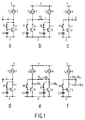
- Figure 1a - c illustrate the ideal transmission of a sample current through two cascaded current memory cells.
- Figure 1a shows the first current memory cell when sampling an input current i
- Figure 1b shows the first current memory cell connected in cascade with the second current memory cell when an output current -i from the first current memory cell is being transferred to the input of the second current memory cell
- Figure 1c shows the second current memory cell when storing the current sensed at its input or outputting the stored current i.
- the first current memory cell comprises an input 1 which receives the input current i and which is coupled to the junction of a current source 2 and the drain electrode of an n-channel field effect transistor T1.
- a switch S1 is connected between the drain and gate electrodes of transistor T1.
- the source electrode of transistor T1 is connected to a negative supply rail 3 while the other end of the current source 2 is connected to a positive supply rail 4.
- a capacitor C1 is connected between the gate electrode of transistor T1 and the negative supply rail 3.
- the capacitor C1 may be the intrinsic gate source capacitance of transistor T1.
- the second current memory cell comprises an n-channel field effect transistor T2 having a switch S2 connected between its drain and gate electrodes and its drain electrode connected via a current source 5 to the positive supply rail 4.
- the source electrode of transistor T2 is connected to the negative supply rail 3 while a capacitor C2 is connected between its gate electrode and the negative supply rail 3. Again the capacitor C2 may be formed by the intrinsic gate source capacitance of transistor T2.
- a further switch S3 couples the drain electrodes of transistors T1 and T2.
- the drain electrode of transistor T2 is connected to an output 6 from which an output current i may be derived.
- further switches may be connected between the input 1 and the junction of transistor T1 and current source 2 and between the output 6 and the junction of transistor T2 and the current source 5.
- the current sources 2 and 5 are arranged to produce equal currents J which enable bidirectional input current to be handled.
- the input currents should have a magnitude of less than J so that the diode connected transistors T1 and T2 do not become reverse biassed.
- switch S1 To sample an input current i the switch S1 is closed and switch S3 is open during a portion ⁇ 1 of each cycle of a clock signal.
- Transistor T1 is consequently connected as a diode and will pass the current J+i.
- the capacitor Cl will be charged through the switch S1 to store a charge which is dependent on the gate source voltage of the transistor T1.
- switch S1 When at the end of the portion ⁇ 1 the switch S1 is opened the charge remains on capacitor C1 and hence causes the transistor T1 to draw the same current J+i.
- Switches S2 and S3 are then closed during a portion ⁇ 2 of the clock signal.
- the current J+i in transistor T1 is then derived from the current sources 2 and 5 resulting in a current J-i being passed through transistor T2 which is now diode connected.
- the capacitor C2 becomes charged to the gate source potential of transistor T2 and when at the end of the portion ⁇ 2 switches S2 and S3 are opened the current through transistor T2 is maintained at the value J-i.
- a current of +i is available at output 6 while switches S2 and S3 are open.
- the current at output 6 is equal to the current applied to input 1 but is delayed in time depending on the sequential operation of the switches S1 to S3.
- the switch S1 would be closed during a first portion of a clock period while switches S2 and S3 are closed during a second portion of the clock period.
- the current i produced at output 6 is equal to the current i applied to input 1 in the previous clock cycle.
- Figure 1d-f illustrates the action of the cascaded memory cells in the same way but includes the effect of error currents produced by charge injection caused by the operation of switches S1 and S2.
- switch S1 is closed and the current i is fed to the diode connected transistor T1 and as a result when switch S1 opens a current J+i should be stored.
- switch S1 opens there is a transfer of charge between its capacitance and that of capacitor C1. This results in an error current of - ⁇ I 1 being produced in transistor T1.
- the current stored in transistor T1 when switch S1 opens become J+i- ⁇ I 1 .
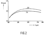
- Figure 2 shows a typical example of the characteristic of current against error current for a current memory cell as shown in Figure la.
- Curve a) is the result of plotting a simulated error current from a computer simulation of the circuit
- curve b) shows the error current which is calculated from an approximate mathematical representation of the device characteristics.
- Figure 2 there is a region of comparatively constant error around an optimum position. The optimum position is not sharp so that this error current may be reasonably constant around the optimum position.
- a wider signal current swing will again reach positions on the curve where the error current is approximately equal for equal current swings about the bias current.
- a possible explanation for the shape of the curve is as follows.
- the optimum bias current varies with process dependent parameters and in order to automatically obtain the optimum bias current a control circuit is needed to derive the bias current.
- the process parameters will be substantially constant and thus the same bias current can be generated for each of the current memory cells and only a single control circuit is necessary to control the generation of the bias currents.
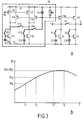
- the circuit arrangement shown in Figure 3 includes a first control arrangement 10 for producing the optimum bias current for the current memory cells.
- the control arrangement shown in Figure 3 is basically two current memory cells connected in cascade but to which only bias currents are applied.
- a first p-channel field effect transistor T10 is connected in series with a first n-channel field effect transistor T11 between a positive supply rail 11 and a negative supply rail 12.
- a first switch S11 is connected between the drain electrode of transistor T11 and its gate electrode while a capacitor C11 is connected between the gate electrode of transistor T11 and the supply rail 12.
- the junction of the drain electrodes of transistors T10 and T11 are connected via a switch S13 to the junction of the drain electrodes of a p-channel field effect transistor T12 and an n-channel field effect transistor T13.
- the source electrode of transistor T12 is connected to the positive supply rail 11 while the source electrode of transistor T13 is connected to the negative supply rail 12.
- a switch S12 is connected between the drain and gate electrodes of transistor T13 while a capacitor C12 is connected between its gate and source electrodes.
- the gate electrodes of transistors T10 and T12 are connected to a bias potential V B .
- Two further p-channel field effect transistors T14 and T15 have their source electrodes connected to the positive supply rail 11.
- the drain electrode of transistor T14 is connected to the drain electrode of transistor T11 while the drain electrode of T15 is connected to the drain electrode of transistor T13.
- the drain electrode of transistor T13 is connected through a switch S14 to one end of a capacitor Cx whose other end is connected to the positive supply rail 11.
- a resistor Rx is connected in parallel with the capacitor Cx and the gate electrodes of transistors T14 and T15 are connected to the junction of the switch S14 and the capacitor Cx.
- This junction is further connected to the gate electrodes of two p channel field effect transistors T16 and T17 which are equivalent to the current sources 2 and 5 of the cascaded current memory cells shown in Figure 1.
- the reference signs for the rest of the cascaded current memory cells are the same as those shown in Figure 1.
- capacitor Cx which is chosen to have a large enough value that charge injection into it has negligible effect is discharged by a large resistor Rx and the cells are biassed by the current in transistors T10 and T12 which are dimensioned such that the current I 1 produced by transistor T10 is smaller than the current I 2 produced by the transistor T12.
- the charge injection errors generate a current ⁇ I 2 - ⁇ I 1 which flows into capacitor Cx on each clock phase ⁇ 1 of the clock which operates the switch S11 to S14.
- transistors T14 and T15 supply additional equal bias currents to the memory cells.
- the currents supplied continue to increase as Cx continues to charge until the maximum of the ⁇ I/I characteristic is reached as shown in Figure 3b.
- ⁇ I 2 produced by current I 2 '
- ⁇ I 1 produced by current I' 1
- no current is available to charge capacitor Cx any further.
- the bias currents of the control circuit 10 stabilise at this value as do the bias currents supplied to other cells on the same chip.
- the current through transistor T14 (and T15) will be equal to J-I 1 , where J is the optimum bias current. Consequently the dimensions of transistors T14 and T15 will have to be scaled appropriately with respect to the bias current generation transistors, such as T16 and T17, in the signal processing current memory cells which will not include equivalent sources to those provided by transistors T10 and T12 in the control circuit 10.
- the optimum bias current is affected by the clock signal amplitude and consequently instead of varying the bias current it is possible to vary the clock signal amplitude to cause the bias current to be the optimum.
- Figure 4 shows a second control arrangement which in this case varies the clock signal amplitude to cause the error characteristic to become symmetrical about the bias current within the current memory cells.
- the arrangement shown in Figure 4 contains two current memory cells which are similar to those in Figure 3 and whose output is fed via the switch S14 to the parallel combination of capacitor Cx and resistor Rx.
- the bias current sources formed by transistors T10 and T12 are now arranged to produce bias currents J1 and J2 which are set symmetrically about the bias current J used by the current memory cells in the signal processing part of the circuitry.
- the additional components in the arrangement shown in Figures 4 are an amplifier 13 which produces a voltage V DD for the clock generator 14.
- the clock generator produces two clock signals ⁇ 1 and ⁇ 2 of the same frequency.
- the switches S11 and S14 are closed during phase ⁇ 1 while the switches S12 and S13 are closed during the phase ⁇ 2.
- the clock voltage V H will start initially as being equal to V DD the voltage on the positive supply rail 11, when capacitor Cx is completely discharged and the error characteristic will be as shown as curve a) in Figure 4b.
- the currents J1 and J2 cause error currents ⁇ J 1 and ⁇ J 2 which are different.
- the difference current will cause capacitor Cx to start to charge.
- This process continues and causes the voltage V H to decrease until the curve approaches curve b) of Figure 4b where ⁇ J 2 is equal to ⁇ J 1 .
- This clock signal is fed to all the other current memory cells in the signal processing circuitry.
- the bias current J will therefore be set at the optimum bias current as far as charge injection error reduction is concerned since the clock signal amplitude is adjusted to make this so.
- the present invention uses the principle of cancelling charge injection errors over two cascaded current memory cells and thus enables a current memory cell having a larger charge injection error to be used whilst still giving reasonable performance.
- this technique should not be combined with other techniques for reducing charge injection error in individual current memory cells though clearly only some charge injection reduction techniques are compatible for example the use of dummy switches would be entirely compatible with the present invention but it would not be possible to use the second technique described by Wegman and Vittoz of tailoring the clock signal voltage to the amplitude of the signal currents in the current memory cells as according to this invention the clock voltage is set to a value which gives the equal and opposite errors in successive cascaded stages.
- the invention has been described using a basic current memory cell of the simplest kind. It is equally applicable to other current memory cells which have circuit enhancements to reduce other inaccuracies within the current memory cell, thus enhancements to produce a more nearly zero output conductance, for example the use of cascode connected transistors could additionally be employed. Further, although the memory transistors shown have been n-channel field effect transistors it is of course equally usable with p-channel field effect transistors as the memory devices, the polarities of the supplies merely being reversed and n-channel devices used as the current sources.
Landscapes
- Dram (AREA)
- Semiconductor Memories (AREA)
- Analogue/Digital Conversion (AREA)
- Filters That Use Time-Delay Elements (AREA)
Description
Claims (6)
- A circuit arrangement for processing electrical signals in the form of sampled analogue currents, the circuit arrangement comprising a first current memory cell having a current input for receiving an input analogue current and a current output for producing a stored analogue current and comprising a first field effect transistor having its drain and gate electrodes coupled via a first switch which is controlled by means of a clock signal such that it is closed during a first portion of a clock period, means for coupling the current input to the drain electrode of the first transistor during the first portion of the clock period, means for coupling the current output to the drain electrode of the first transistor during a second portion of the clock period, and means for feeding a first bias current to the drain electrode of the first transistor, a second current memory cell connected in cascade with said first current memory cell, said second current memory cell having a current input for receiving an input analogue current and a current output for producing a stored analogue current and comprising a second field effect transistor having its drain and gate electrodes coupled via a second switch which is controlled by means of a clock signal such that it is closed during a second portion of the clock period, means for coupling the current input to the drain electrode of the second transistor during the second portion of the clock period, means for coupling the current output to the drain electrode of the transistor during the first portion of the clock period, and means for feeding a second bias current to the drain electrode of the transistor, characterised by means for causing the magnitude of the first and second bias currents to be such that errors due to charge injection in the first current memory cell are substantially cancelled by oppositely signed errors in the second current memory cell.
- A circuit arrangement as claimed in Claim 1 comprising a control circuit for adjusting the bias current magnitude in the first and second current memory cells, the control circuit comprising third and fourth current memory cells connected in cascade, the third and fourth current memory cells each comprising a bias current source, the bias current sources in the third and fourth current memory cells producing mutually different bias currents, means for detecting an output current produced at the output of the fourth current memory cell and deriving therefrom a control signal to control two further current sources, one for each of the third and fourth current memory cells, and each producing substantially the same current, such that the error current tends to a minimum value, and means for applying the control signal to the first and second current memory cells to adjust the magnitude of the bias current produced in the first and second current memory cells.
- A circuit arrangement as claimed in Claim 2 wherein the control signal is derived by charging a capacitor by the output current of the fourth current memory cell and using the voltage across the capacitor to control the currents produced by the two further current sources.
- A circuit arrangement as claimed in Claim 1 comprising control means for controlling the amplitude of the clock signal to cause the magnitude of the bias current to be such that errors due to charge injection in one current memory cell are substantially cancelled by oppositely signed errors in the second current memory.
- A circuit arrangement as claimed in Claim 4 in which the control means comprises third and fourth current memory cells connected in cascade, the third and fourth current memory cells being of the same form as the first and second current memory cells and each including a bias current source, the bias current sources in the third and fourth current memory cells producing mutually different currents, means for deriving a control signal from the output current of the fourth current memory cell, means for applying the control signal to a clock signal generator to control the amplitude of the clock signals produced, and means for applying the clock signals to the switches to control their operation, the control signal being such that the controlled amplitude of the clock signals cause substantially equal charge injection induced error currents to be produced in the first and second current memory cells.
- A circuit arrangement as claimed in Claim 5 in which the control signal deriving means comprises a capacitor which is charged by the output current of the fourth memory cell, the control signal being the voltage across the capacitor.
Applications Claiming Priority (2)
| Application Number | Priority Date | Filing Date | Title |
|---|---|---|---|
| GB9204763 | 1992-03-05 | ||
| GB929204763A GB9204763D0 (en) | 1992-03-05 | 1992-03-05 | Signal processing arrangements |
Publications (3)
| Publication Number | Publication Date |
|---|---|
| EP0559282A2 EP0559282A2 (en) | 1993-09-08 |
| EP0559282A3 EP0559282A3 (en) | 1994-09-28 |
| EP0559282B1 true EP0559282B1 (en) | 1998-06-03 |
Family
ID=10711538
Family Applications (1)
| Application Number | Title | Priority Date | Filing Date |
|---|---|---|---|
| EP93200562A Expired - Lifetime EP0559282B1 (en) | 1992-03-05 | 1993-03-01 | Signal processing arrangements |
Country Status (5)
| Country | Link |
|---|---|
| US (1) | US5349245A (en) |
| EP (1) | EP0559282B1 (en) |
| JP (1) | JPH0621766A (en) |
| DE (1) | DE69318866T2 (en) |
| GB (1) | GB9204763D0 (en) |
Families Citing this family (17)
| Publication number | Priority date | Publication date | Assignee | Title |
|---|---|---|---|---|
| GB9318640D0 (en) * | 1993-09-08 | 1993-10-27 | Philips Electronics Uk Ltd | Integrator |
| GB9500648D0 (en) * | 1995-01-13 | 1995-03-08 | Philips Electronics Uk Ltd | Switched current differentiator |
| US5572153A (en) * | 1995-03-03 | 1996-11-05 | Lucent Technologies Inc. | Low offset comparators based on current copiers |
| GB9517790D0 (en) * | 1995-08-31 | 1995-11-01 | Philips Electronics Uk Ltd | Switched current circuits |
| US5760616A (en) * | 1995-09-05 | 1998-06-02 | Lucent Technologies, Inc. | Current copiers with improved accuracy |
| US5783952A (en) * | 1996-09-16 | 1998-07-21 | Atmel Corporation | Clock feedthrough reduction system for switched current memory cells |
| US5959470A (en) * | 1997-08-25 | 1999-09-28 | Texas Instruments Incorporated | Operational amplifier with two sample and hold circuits |
| GB9720740D0 (en) * | 1997-10-01 | 1997-12-03 | Philips Electronics Nv | Switched-current memory |
| GB9720712D0 (en) * | 1997-10-01 | 1997-11-26 | Philips Electronics Nv | Current comparator |
| FR2770955B1 (en) * | 1997-11-12 | 2000-01-07 | Suisse Electronique Microtech | CELL COMPRISING A PSEUDO-CAPACITY, PARTICULARLY FOR ARTIFICIAL RETINA |
| US6028466A (en) * | 1998-02-05 | 2000-02-22 | Lucent Technologies Inc. | Integrated circuit including high transconductance voltage clamp |
| KR20000003558A (en) | 1998-06-29 | 2000-01-15 | 김영환 | Pulse generator |
| CN101257284B (en) * | 2002-01-17 | 2011-10-19 | 株式会社半导体能源研究所 | Semiconductor device |
| US10720541B2 (en) | 2012-06-26 | 2020-07-21 | Lockheed Martin Corporation | Foldable solar tracking system, assembly and method for assembly, shipping and installation of the same |
| US9496822B2 (en) | 2012-09-24 | 2016-11-15 | Lockheed Martin Corporation | Hurricane proof solar tracker |
| US9654310B1 (en) * | 2016-11-19 | 2017-05-16 | Nxp Usa, Inc. | Analog delay cell and tapped delay line comprising the analog delay cell |
| CN108963999B (en) * | 2018-08-07 | 2020-02-14 | 中国航空工业集团公司雷华电子技术研究所 | Surge current suppressor |
Family Cites Families (5)
| Publication number | Priority date | Publication date | Assignee | Title |
|---|---|---|---|---|
| GB2209895B (en) * | 1987-09-16 | 1991-09-25 | Philips Electronic Associated | A circuit arrangement for storing sampled analogue electrical currents |
| GB2225910A (en) * | 1988-12-08 | 1990-06-13 | Philips Electronic Associated | Processing sampled analogue electrical signals |
| GB2234835A (en) * | 1989-08-07 | 1991-02-13 | Philips Electronic Associated | Intergrator circuit |
| GB2235799A (en) * | 1989-09-06 | 1991-03-13 | Philips Electronic Associated | Differentiator circuit |
| US5296752A (en) * | 1991-05-08 | 1994-03-22 | U.S. Philips Corporation | Current memory cell |
-
1992
- 1992-03-05 GB GB929204763A patent/GB9204763D0/en active Pending
-
1993
- 1993-03-01 EP EP93200562A patent/EP0559282B1/en not_active Expired - Lifetime
- 1993-03-01 US US08/024,597 patent/US5349245A/en not_active Expired - Fee Related
- 1993-03-01 DE DE69318866T patent/DE69318866T2/en not_active Expired - Fee Related
- 1993-03-04 JP JP5043915A patent/JPH0621766A/en active Pending
Also Published As
| Publication number | Publication date |
|---|---|
| EP0559282A2 (en) | 1993-09-08 |
| DE69318866D1 (en) | 1998-07-09 |
| US5349245A (en) | 1994-09-20 |
| EP0559282A3 (en) | 1994-09-28 |
| DE69318866T2 (en) | 1998-12-24 |
| GB9204763D0 (en) | 1992-04-15 |
| JPH0621766A (en) | 1994-01-28 |
Similar Documents
| Publication | Publication Date | Title |
|---|---|---|
| US5349245A (en) | Signal processing arrangements | |
| KR100466082B1 (en) | Clock feedthrough reduction system for switched current memory cells | |
| EP0540052B1 (en) | Ripple-free phase detector using two sample-and-hold circuits | |
| US4585956A (en) | Switched capacitor feedback sample-and-hold circuit | |
| US4484089A (en) | Switched-capacitor conductance-control of variable transconductance elements | |
| US5400273A (en) | Analog current memory | |
| US4779012A (en) | Track-and-hold amplifier | |
| KR950014094B1 (en) | Sampled Analog Electrical Signal Processing Method and Apparatus | |
| KR0161512B1 (en) | Integrator circuit | |
| US5023489A (en) | Integrator circuit | |
| JP2975378B2 (en) | Track and hold circuit | |
| US6437620B1 (en) | Circuit and method for multi-phase alignment | |
| US5767708A (en) | Current integrator circuit with conversion of an input current into a capacitive charging current | |
| US5534815A (en) | Switching circuit for signal sampling with reduced residual charge effects | |
| Vittoz | Microwatt switched capacitor circuit design | |
| EP0107337B1 (en) | Improvements in or relating to sample-and-hold circuits and methods | |
| EP1014288A1 (en) | Improved method and circuit arrangement for signal processing | |
| EP0552883B1 (en) | High speed sample and hold signal generator | |
| JP2000132989A (en) | Track hold circuit | |
| EP0696804B1 (en) | Sampling and holding circuit | |
| JP2943702B2 (en) | Peak hold circuit for burst communication | |
| Zweigle et al. | High accuracy switched-current circuits using an improved dynamic mirror | |
| JPS63219219A (en) | Switched capacitor circuit | |
| Zweigle et al. | High Accuracy Switched-Current Circuits Using an | |
| Wang et al. | CMOS analog implementation of a discrete-time 9-tap FIR filter with circular buffer architecture |
Legal Events
| Date | Code | Title | Description |
|---|---|---|---|
| PUAI | Public reference made under article 153(3) epc to a published international application that has entered the european phase |
Free format text: ORIGINAL CODE: 0009012 |
|
| AK | Designated contracting states |
Kind code of ref document: A2 Designated state(s): DE FR GB IT |
|
| PUAL | Search report despatched |
Free format text: ORIGINAL CODE: 0009013 |
|
| AK | Designated contracting states |
Kind code of ref document: A3 Designated state(s): DE FR GB IT |
|
| 17P | Request for examination filed |
Effective date: 19950328 |
|
| 17Q | First examination report despatched |
Effective date: 19970131 |
|
| GRAG | Despatch of communication of intention to grant |
Free format text: ORIGINAL CODE: EPIDOS AGRA |
|
| GRAG | Despatch of communication of intention to grant |
Free format text: ORIGINAL CODE: EPIDOS AGRA |
|
| GRAG | Despatch of communication of intention to grant |
Free format text: ORIGINAL CODE: EPIDOS AGRA |
|
| GRAH | Despatch of communication of intention to grant a patent |
Free format text: ORIGINAL CODE: EPIDOS IGRA |
|
| GRAH | Despatch of communication of intention to grant a patent |
Free format text: ORIGINAL CODE: EPIDOS IGRA |
|
| GRAA | (expected) grant |
Free format text: ORIGINAL CODE: 0009210 |
|
| AK | Designated contracting states |
Kind code of ref document: B1 Designated state(s): DE FR GB IT |
|
| PG25 | Lapsed in a contracting state [announced via postgrant information from national office to epo] |
Ref country code: IT Free format text: LAPSE BECAUSE OF FAILURE TO SUBMIT A TRANSLATION OF THE DESCRIPTION OR TO PAY THE FEE WITHIN THE PRE;WARNING: LAPSES OF ITALIAN PATENTS WITH EFFECTIVE DATE BEFORE 2007 MAY HAVE OCCURRED AT ANY TIME BEFORE 2007. THE CORRECT EFFECTIVE DATE MAY BE DIFFERENT FROM THE ONE RECORDED.SCRIBED TIME-LIMIT Effective date: 19980603 |
|
| REF | Corresponds to: |
Ref document number: 69318866 Country of ref document: DE Date of ref document: 19980709 |
|
| ET | Fr: translation filed | ||
| RAP4 | Party data changed (patent owner data changed or rights of a patent transferred) |
Owner name: KONINKLIJKE PHILIPS ELECTRONICS N.V. Owner name: PHILIPS ELECTRONICS UK LIMITED |
|
| REG | Reference to a national code |
Ref country code: FR Ref legal event code: CD |
|
| PLBE | No opposition filed within time limit |
Free format text: ORIGINAL CODE: 0009261 |
|
| STAA | Information on the status of an ep patent application or granted ep patent |
Free format text: STATUS: NO OPPOSITION FILED WITHIN TIME LIMIT |
|
| 26N | No opposition filed | ||
| PGFP | Annual fee paid to national office [announced via postgrant information from national office to epo] |
Ref country code: FR Payment date: 20010326 Year of fee payment: 9 |
|
| PGFP | Annual fee paid to national office [announced via postgrant information from national office to epo] |
Ref country code: GB Payment date: 20010330 Year of fee payment: 9 |
|
| PGFP | Annual fee paid to national office [announced via postgrant information from national office to epo] |
Ref country code: DE Payment date: 20010516 Year of fee payment: 9 |
|
| REG | Reference to a national code |
Ref country code: GB Ref legal event code: IF02 |
|
| PG25 | Lapsed in a contracting state [announced via postgrant information from national office to epo] |
Ref country code: GB Free format text: LAPSE BECAUSE OF NON-PAYMENT OF DUE FEES Effective date: 20020301 |
|
| PG25 | Lapsed in a contracting state [announced via postgrant information from national office to epo] |
Ref country code: DE Free format text: LAPSE BECAUSE OF NON-PAYMENT OF DUE FEES Effective date: 20021001 |
|
| GBPC | Gb: european patent ceased through non-payment of renewal fee |
Effective date: 20020301 |
|
| PG25 | Lapsed in a contracting state [announced via postgrant information from national office to epo] |
Ref country code: FR Free format text: LAPSE BECAUSE OF NON-PAYMENT OF DUE FEES Effective date: 20021129 |
|
| REG | Reference to a national code |
Ref country code: FR Ref legal event code: ST |