EP0556655B1 - Device and method for testing optical elements - Google Patents
Device and method for testing optical elements Download PDFInfo
- Publication number
- EP0556655B1 EP0556655B1 EP93101739A EP93101739A EP0556655B1 EP 0556655 B1 EP0556655 B1 EP 0556655B1 EP 93101739 A EP93101739 A EP 93101739A EP 93101739 A EP93101739 A EP 93101739A EP 0556655 B1 EP0556655 B1 EP 0556655B1
- Authority
- EP
- European Patent Office
- Prior art keywords
- optical element
- light
- array
- photosensitive elements
- optical
- Prior art date
- Legal status (The legal status is an assumption and is not a legal conclusion. Google has not performed a legal analysis and makes no representation as to the accuracy of the status listed.)
- Expired - Lifetime
Links
- 230000003287 optical effect Effects 0.000 title claims abstract description 55
- 238000000034 method Methods 0.000 title claims description 20
- 238000012360 testing method Methods 0.000 title description 15
- 230000007547 defect Effects 0.000 claims abstract description 20
- 238000005286 illumination Methods 0.000 claims description 10
- 238000011156 evaluation Methods 0.000 claims description 9
- 239000013307 optical fiber Substances 0.000 claims description 2
- 230000000903 blocking effect Effects 0.000 claims 1
- 230000001360 synchronised effect Effects 0.000 abstract 1
- 230000010354 integration Effects 0.000 description 5
- 238000004519 manufacturing process Methods 0.000 description 4
- 238000003384 imaging method Methods 0.000 description 3
- 238000012545 processing Methods 0.000 description 3
- 230000000750 progressive effect Effects 0.000 description 3
- 239000000835 fiber Substances 0.000 description 2
- 238000007689 inspection Methods 0.000 description 2
- 238000001228 spectrum Methods 0.000 description 2
- 238000013459 approach Methods 0.000 description 1
- 238000007796 conventional method Methods 0.000 description 1
- 239000002537 cosmetic Substances 0.000 description 1
- 230000001419 dependent effect Effects 0.000 description 1
- 238000001514 detection method Methods 0.000 description 1
- 238000011161 development Methods 0.000 description 1
- 230000018109 developmental process Effects 0.000 description 1
- 229910052736 halogen Inorganic materials 0.000 description 1
- 150000002367 halogens Chemical class 0.000 description 1
- 238000003780 insertion Methods 0.000 description 1
- 230000037431 insertion Effects 0.000 description 1
- 239000000463 material Substances 0.000 description 1
- 238000012986 modification Methods 0.000 description 1
- 230000004048 modification Effects 0.000 description 1
- 230000035945 sensitivity Effects 0.000 description 1
- 238000002834 transmittance Methods 0.000 description 1
- 230000000007 visual effect Effects 0.000 description 1
Images


Classifications
-
- G—PHYSICS
- G01—MEASURING; TESTING
- G01M—TESTING STATIC OR DYNAMIC BALANCE OF MACHINES OR STRUCTURES; TESTING OF STRUCTURES OR APPARATUS, NOT OTHERWISE PROVIDED FOR
- G01M11/00—Testing of optical apparatus; Testing structures by optical methods not otherwise provided for
- G01M11/02—Testing optical properties
- G01M11/0242—Testing optical properties by measuring geometrical properties or aberrations
- G01M11/0278—Detecting defects of the object to be tested, e.g. scratches or dust
-
- G—PHYSICS
- G01—MEASURING; TESTING
- G01M—TESTING STATIC OR DYNAMIC BALANCE OF MACHINES OR STRUCTURES; TESTING OF STRUCTURES OR APPARATUS, NOT OTHERWISE PROVIDED FOR
- G01M11/00—Testing of optical apparatus; Testing structures by optical methods not otherwise provided for
- G01M11/02—Testing optical properties
- G01M11/0242—Testing optical properties by measuring geometrical properties or aberrations
- G01M11/0257—Testing optical properties by measuring geometrical properties or aberrations by analyzing the image formed by the object to be tested
- G01M11/0264—Testing optical properties by measuring geometrical properties or aberrations by analyzing the image formed by the object to be tested by using targets or reference patterns
-
- G—PHYSICS
- G01—MEASURING; TESTING
- G01N—INVESTIGATING OR ANALYSING MATERIALS BY DETERMINING THEIR CHEMICAL OR PHYSICAL PROPERTIES
- G01N21/00—Investigating or analysing materials by the use of optical means, i.e. using sub-millimetre waves, infrared, visible or ultraviolet light
- G01N21/84—Systems specially adapted for particular applications
- G01N21/88—Investigating the presence of flaws or contamination
-
- G—PHYSICS
- G01—MEASURING; TESTING
- G01N—INVESTIGATING OR ANALYSING MATERIALS BY DETERMINING THEIR CHEMICAL OR PHYSICAL PROPERTIES
- G01N21/00—Investigating or analysing materials by the use of optical means, i.e. using sub-millimetre waves, infrared, visible or ultraviolet light
- G01N21/84—Systems specially adapted for particular applications
- G01N21/88—Investigating the presence of flaws or contamination
- G01N21/8806—Specially adapted optical and illumination features
Definitions
- the invention relates to a method and a system for testing optical elements, made of optical material so as to determine the presence of any defects, and to decide whether such elements are of adequate quality or have to be discarded.
- the system is suited to test lenses, over a wide range of diopters, possibly also with cylindrical components.
- the system is suited for the testing of surface defects and also for detecting other internal faults.
- the system is suitable for use in the inspection of optical elements during the production process, and for the grading of such elements.
- Optical components must be tested prior to their utilization. Conventionally, the testing of optical components is carried out by trained personnel by visual manual inspection. This approach is not quantitative in nature, and thus can not be carried out objectively and reliably. The performance varies with different inspectors and with the same inspector from time to time.
- the lenses may be positive or negative, spherical, cylindrical or both, aspheric and progressive.
- Most solutions have difficulties in adapting to different batches of lenses that have different geometrical properties, using different illumination geometries for each batch, thus consuming time in arranging the set up between different batches.
- optical transparent elements which may have cylindrical component, progressive lenses, aspheric lenses, etc., so as to detect surface and internal defects.
- a method for such testing The system can be used in a mass production and gives rapid and reliable results. Means are advantageously provided for the automatic evaluation of the test results and for the grading of the optical elements.
- the basic features of the method of the invention comprises a scanning of the lens by the means of one,- or more light beams, so that any surface or internal defects scatter the light of the incident beam or beams, which scattered light is collected by a photo sensitive element, such as a CCD camera, the output of which is indicative of the presence or the absence of the defects, and the severity of such defects.
- a photo sensitive element such as a CCD camera
- the method is applicable for the testing of lenses having a wide range of diopters, and which may have a variety of cylindrical components., and for the automatic reliable and rapid evaluation so as to determine any possible production defects.
- the surface of the lens is scanned sector wise so as to cover the entire surface.
- the system provides one or more wedge shaped light beams, which are rotated and which illuminate simultaneously the same narrow strip of the lens surface. Any defect of the lens, such as surface scratches, irregularities and the like, scatter some of the light toward a light sensitive element, which is generally a suitable CCD camera, while in the absence of such defects light coming from the light source will not reach such a photoelectric array.
- the wedge shaped light beam aimed at the diameter of the lens is incident onto this diameter at a rather wide range of incidence angles, so that the light is scattered by a variety of flaws, which light passes through a suitable mask, which rotates synchronously with the scanning light beam and only light due to scattering from flaws passes said mask and reaches the said CCD camera.
- the mask allows illuminating the tested lens at relatively small angles without imaging the light source, and also blocks out images resulting from internal light reflections between the lens surfaces. The method gives reliable results and can be used to test defects according to the ANSI, DIN and other standards.
- the CCD camera is operated in a single shot mode wherein integration time can be controlled.
- the time is advantageously set to a period that equals one or more whole scanning revolutions, and at the end of such scan or sequence of scans, the information collected in the camera frame is fed as standard video to a frame grabber and evaluation system.
- an image processing algorithm which enhances the lens flaws, recognizes them, evaluates them according to predetermined parameters and decides whether to accept or to discard the tested lens.
- the testing sequence can be actuated by the insertion of the lens to be tested in place in the test system.
- the lenses are tested by means of white light, i.e. over a wide range of wavelengths, which is closest to the conditions under which the lens is used in spectacles or the like.
- the invention is illustrated by means of a system where two such parallel wedge shaped light beams are directed at the diameter of the lens.
- An important part of the system is the rotation mechanism, which comprises the two sub systems LS, the light source, and rotating light transformer and scanning device, LTS.
- the system further comprises the imaging system IS.
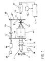
- the embodiment of the system of the invention comprises a lamp 11, a heat absorbing filter 12, a fan 13 for removing heat, an adjustable power supply 14.
- the light combing out of the lamp passes through the condenser 15 and enters the LTS 40, which is driven by the means of the timing wheel 16, which is connected with the timing wheel 17 by timing belt 18, this mechanism being actuated by motor 19 driven by motor controller 25.
- the motor is connected to shaft 20, the end of which is connected with similar mechanism, comprising a rotating mask 21, which is actuated via timing wheels 22 and 23, connected by belt 24.
- the light coming from the condenser 15 passes through rotating light transformer and scanning unit 40.
- Fig. 2 is a perspective view, showing the arrangement of part of the system set out in Fig. 1, where the parts are designed by identical numbers.
- FIG. 3 and 4 One embodiment is shown in Fig. 3 and 4 where 41 is a housing, the entry port of which, 42 is a hollow shaft housing the round light entrance member 43 of the light transformer, which passes the light via fiber bundles 44 and 45 to members 46 and 47, which emits the light linearly towards cylindrical lenses 50 and 51, which focus the light beams 48 and 49, in the vicinity of the frontal surface of the tested lens 52, in various angles and intensities which are set by using to two sets of three at the imaging system IS, which comprises a lens 70, a video camera 71, camera timing control 72, and image grabber and processor 73.
- the only light that reaches the CCD in the camera is the scattered light from the imperfections of the tested optical element.
- the system advantageously comprises beam splitters 62 and 63, which reflect back part of the light beams towards the dark background 61.
- the degree of illumination of the background is easily controlled by varying at will the coefficients of transmittance of the beam splitters.
- the partial illumination of the dark background is a requirement of certain standard of lens testing methods.
- angles b and g When two light beam groups are used they illuminate the lens simultaneously, at the angles b and g, by adjusting these angles, the illumination can be made to vary within a rather wide range of angles.
- angle a will be in the range of about 20° to about 35°.
- Angles b and g will generally be in the range from 15° to about 25°.
- the importance of the angles of the incident beams is in that various types of defects are more sensitive to illumination at a given angle than at another, and thus by using various angles of the light beams, the detection capability of the system is enhanced.
- a system was constructed according to the above principles, and the following data are to be constructed in a non restrictive manner. According to the nature of the tested optical element, such as type of lens, its diameter, etc., variations and modifications of the system may be restored to, and components with widely different values can be used.
- a 50 W halogen projector As light source there was used a 50 W halogen projector, with its main light spectrum in the 400 to 800 nm range.
- the bundles of optical fibers have a diameter of about 8.5 mm, and an effective surface area of about 56 mm .
- Fibers having a uniform attenuation of light over the spectrum 400 to 1200 nm was used.
- a wide range of rotation speeds can be used, which will generally be in the range of from about 125 RPM to about 1500 RPM. Good results were obtained with a model where the rate of revolution was 375 RPM.
- the mask is as illustrated in Fig. 2.
- the linear light beam directed at the diameter of the lens spreads out from the center towards the edge of the lens. This spread forms on the lens surface two illumination sectors. These sectors and the mask sectors rotate synchronously.
- the opening angle of the mask sectors is dictated by the said light spread.
- the two lenses used for the focusing of the light beams inside the inspected lens are cylindrical lenses of focal lengths 12 mm.
- the opening angles of each of the two beam groups was 32°, and the angle b and g were 15° and 19°, respectively.
- the principle of the operation of the camera timing and exposure control ia as follows:
- the camera is provided with integration time control means.
- the integration period continues as long as the integration signal is present.
- Information gathered in the CCD passes through the image grabber in standard video format, starting with the first vertical pulse after cessation of the integration signal.
- the described method can be alternatively realized using any optical and/or electro optical combination to implement the said optical element illumination and evaluation method, within the scope of the claims.
Landscapes
- Physics & Mathematics (AREA)
- General Physics & Mathematics (AREA)
- Chemical & Material Sciences (AREA)
- Analytical Chemistry (AREA)
- Life Sciences & Earth Sciences (AREA)
- Health & Medical Sciences (AREA)
- Geometry (AREA)
- Biochemistry (AREA)
- General Health & Medical Sciences (AREA)
- Immunology (AREA)
- Pathology (AREA)
- Testing Of Optical Devices Or Fibers (AREA)
- Testing Or Measuring Of Semiconductors Or The Like (AREA)
- Investigating Materials By The Use Of Optical Means Adapted For Particular Applications (AREA)
- Tests Of Electronic Circuits (AREA)
Abstract
Description
- The invention relates to a method and a system for testing optical elements, made of optical material so as to determine the presence of any defects, and to decide whether such elements are of adequate quality or have to be discarded.
- The system is suited to test lenses, over a wide range of diopters, possibly also with cylindrical components. This includes various types of lenses, such as progressive lenses, aspheric ones, optical filters, etc.
- The system is suited for the testing of surface defects and also for detecting other internal faults. The system is suitable for use in the inspection of optical elements during the production process, and for the grading of such elements.
- Optical components must be tested prior to their utilization. Conventionally, the testing of optical components is carried out by trained personnel by visual manual inspection. This approach is not quantitative in nature, and thus can not be carried out objectively and reliably. The performance varies with different inspectors and with the same inspector from time to time.
- Efforts have been made to develop methods and devices for automatic and objective testing of transparent optical components. The following patents deal with the subject matter: DE-A-36 20 146 (corresponding to US-A-4 841 139); DE-A-36 20 108 (corresponding to US-A-4 822 165); DE-A-36 20 129 (corresponding to US-A-4 815 844); DD-241120; US-A-3 988 068; and GB-34851/72 (corresponding to US-A-3 892 494).
- These have significant drawbacks. The proposed solutions in these patents are not cost effective in the sense that they are too complex and slow for use in mass production lines. Systems that utilize complex scanning means are too slow to inspect hundreds of lenses per hour, as required in such lines.
- Another problem arises from sensitivity to various lens parameters. The lenses may be positive or negative, spherical, cylindrical or both, aspheric and progressive. Most solutions have difficulties in adapting to different batches of lenses that have different geometrical properties, using different illumination geometries for each batch, thus consuming time in arranging the set up between different batches.
- Yet, a serious problem arises from the illumination methodology itself, patents using light sources with characteristics that are different in nature from the recommendation in the various cosmetic standards, lead to differences in the defects appearance in respect to their appearance in daily use of lenses, thus causing to a serious reliability problem by producing artifacts that are not detectable in daily use. Furthermore, some of the illumination methods are sensitive to different defects locations causing difficulties in simultaneously detecting defects in both faces and inside the lens and therefore resulting in non homogeneous yield.
- The present patent overcomes these difficulties and shortcomings of the said previous patents and publications by providing a method as defined in claim 1, a system as defined in claim 8 and the use of said system as defined in
claim 16. - Further developments of the invention are defined in the dependent claims.
- There is provided a system for testing optical transparent elements, which may have cylindrical component, progressive lenses, aspheric lenses, etc., so as to detect surface and internal defects. There is further provided a method for such testing. The system can be used in a mass production and gives rapid and reliable results. Means are advantageously provided for the automatic evaluation of the test results and for the grading of the optical elements.
- The basic features of the method of the invention comprises a scanning of the lens by the means of one,- or more light beams, so that any surface or internal defects scatter the light of the incident beam or beams, which scattered light is collected by a photo sensitive element, such as a CCD camera, the output of which is indicative of the presence or the absence of the defects, and the severity of such defects.
- The method is applicable for the testing of lenses having a wide range of diopters, and which may have a variety of cylindrical components., and for the automatic reliable and rapid evaluation so as to determine any possible production defects. According to the method of the invention the surface of the lens is scanned sector wise so as to cover the entire surface.
The system provides one or more wedge shaped light beams, which are rotated and which illuminate simultaneously the same narrow strip of the lens surface. Any defect of the lens, such as surface scratches, irregularities and the like, scatter some of the light toward a light sensitive element, which is generally a suitable CCD camera, while in the absence of such defects light coming from the light source will not reach such a photoelectric array. - The wedge shaped light beam aimed at the diameter of the lens is incident onto this diameter at a rather wide range of incidence angles, so that the light is scattered by a variety of flaws, which light passes through a suitable mask, which rotates synchronously with the scanning light beam and only light due to scattering from flaws passes said mask and reaches the said CCD camera. The mask allows illuminating the tested lens at relatively small angles without imaging the light source, and also blocks out images resulting from internal light reflections between the lens surfaces. The method gives reliable results and can be used to test defects according to the ANSI, DIN and other standards.
- The CCD camera is operated in a single shot mode wherein integration time can be controlled. The time is advantageously set to a period that equals one or more whole scanning revolutions, and at the end of such scan or sequence of scans, the information collected in the camera frame is fed as standard video to a frame grabber and evaluation system.
- Advantageously there is employed an image processing algorithm, which enhances the lens flaws, recognizes them, evaluates them according to predetermined parameters and decides whether to accept or to discard the tested lens.
- According to a preferred embodiment, the testing sequence can be actuated by the insertion of the lens to be tested in place in the test system.
- The use of a mono shot camera simplifies the computation and improves the signal to noise ratio. It is advantageous to hold the lens in place, while the light beam is rotated so as to scan the lens surface by wedge shaped beam or beams. The lenses are tested by means of white light, i.e. over a wide range of wavelengths, which is closest to the conditions under which the lens is used in spectacles or the like.
- The system and method of the invention are described by way of illustration, in a non restrictive manner, with reference to the inclosed drawings, which are schematic and not according to scale., in which:
- Fig. 1 is a schematic side view of an embodiment of a system of the invention;
- Fig. 2 is a perspective view of the rotating light transformer and scanning device of the system;
- Fig. 3 is a perspective view of the sub system for producing two linear light beams parallel with each other in a plane;
- Fig. 4 is a sectional side view of the preferred rotating light source and beams incident on the lens being tested.
- Although the testing of the optical elements can be carried out by means of a single rotating mirror, the invention is illustrated by means of a system where two such parallel wedge shaped light beams are directed at the diameter of the lens. An important part of the system is the rotation mechanism, which comprises the two sub systems LS, the light source, and rotating light transformer and scanning device, LTS. The system further comprises the imaging system IS.
- As shown in Fig. 1, the embodiment of the system of the invention comprises a
lamp 11, aheat absorbing filter 12, afan 13 for removing heat, anadjustable power supply 14. The light combing out of the lamp passes through thecondenser 15 and enters the LTS 40, which is driven by the means of thetiming wheel 16, which is connected with thetiming wheel 17 bytiming belt 18, this mechanism being actuated bymotor 19 driven bymotor controller 25. The motor is connected toshaft 20, the end of which is connected with similar mechanism, comprising arotating mask 21, which is actuated viatiming wheels belt 24. The light coming from thecondenser 15 passes through rotating light transformer and scanningunit 40. - Fig. 2 is a perspective view, showing the arrangement of part of the system set out in Fig. 1, where the parts are designed by identical numbers.
- One embodiment is shown in Fig. 3 and 4 where 41 is a housing, the entry port of which, 42 is a hollow shaft housing the round
light entrance member 43 of the light transformer, which passes the light viafiber bundles members cylindrical lenses light beams lens 52, in various angles and intensities which are set by using to two sets of three at the imaging system IS, which comprises alens 70, avideo camera 71,camera timing control 72, and image grabber andprocessor 73. The only light that reaches the CCD in the camera is the scattered light from the imperfections of the tested optical element. Each of thelight beams cylindrical lenses - The system advantageously comprises
beam splitters dark background 61. The degree of illumination of the background is easily controlled by varying at will the coefficients of transmittance of the beam splitters. The partial illumination of the dark background is a requirement of certain standard of lens testing methods. - When two light beam groups are used they illuminate the lens simultaneously, at the angles b and g, by adjusting these angles, the illumination can be made to vary within a rather wide range of angles. Generally the angle a will be in the range of about 20° to about 35°. Angles b and g will generally be in the range from 15° to about 25°. The importance of the angles of the incident beams is in that various types of defects are more sensitive to illumination at a given angle than at another, and thus by using various angles of the light beams, the detection capability of the system is enhanced.
- A system was constructed according to the above principles, and the following data are to be constructed in a non restrictive manner. According to the nature of the tested optical element, such as type of lens, its diameter, etc., variations and modifications of the system may be restored to, and components with widely different values can be used.
- As light source there was used a 50 W halogen projector, with its main light spectrum in the 400 to 800 nm range. The bundles of optical fibers have a diameter of about 8.5 mm, and an effective surface area of about 56 mm . Fibers having a uniform attenuation of light over the spectrum 400 to 1200 nm was used. A wide range of rotation speeds can be used, which will generally be in the range of from about 125 RPM to about 1500 RPM. Good results were obtained with a model where the rate of revolution was 375 RPM.
- There is used a 15 mm focal length condenser, and the mask is as illustrated in Fig. 2. As the surface area of the inspected lens is curved, the linear light beam directed at the diameter of the lens spreads out from the center towards the edge of the lens. This spread forms on the lens surface two illumination sectors. These sectors and the mask sectors rotate synchronously. The opening angle of the mask sectors is dictated by the said light spread. The two lenses used for the focusing of the light beams inside the inspected lens are cylindrical lenses of
focal lengths 12 mm. The opening angles of each of the two beam groups was 32°, and the angle b and g were 15° and 19°, respectively. There was used a CCD camera of the PULNIX 765E type, with a lens f = 25 mm, D = f25 mm at its front. The principle of the operation of the camera timing and exposure control ia as follows: - The camera is provided with integration time control means. The integration period continues as long as the integration signal is present. Information gathered in the CCD passes through the image grabber in standard video format, starting with the first vertical pulse after cessation of the integration signal.
- There was used an image grabbing and processing subsystem which consists of MATROX - Image series installed in an IBM/AT compatible computer, and evaluation of the incoming signals resulting from lens imperfections was carried out with the help of a suitable algorithm, using conventional techniques of image processing and evaluation.
- The described method can be alternatively realized using any optical and/or electro optical combination to implement the said optical element illumination and evaluation method, within the scope of the claims.
Claims (16)
- A method for evaluation of transparent optical elements (52) so as to detect surface and other defects of said optical element (52) and to grade the optical elements (52) according to predetermined criteria, comprising the steps of:(a) generating a beam of white light having a wedge-shaped longitudinal section and a linear axis,(b) illuminating said optical element (52) by focusing the beam onto a diameter of said optical element (52) to intersect said optical element (52) with said beam,(c) rotating the light beam with respect to said optical element (52) and scanning its entire surface at least once,(d) passing scattered light resulting from defects of said optical element (52) via a mask (21) disposed between said optical element (52) and an array (71) of photosensitive elements, and rotating said mask (21) in synchronisation with the rotation of the light beam so that said scattered light is passed to said array (71) of photosensitive elements while blocking out direct light from said light beam so that such light does not reach said array (71) of photosensitive elements (71),(e) passing signals resulting from said scattered light in said array (71) of photosensitive elements to an image grabbing and evaluation unit (73), and(f) evaluating the quality of said optical element (52).
- A method according to claim 1, wherein a mask (21) is used with openings in the form of segments.
- A method according to claim 1 or 2, wherein the wedge angle of said light beam is from 5 degrees to 35 degrees and the angle of the axis of said beam to the axis of said optical element (52) is from 10 degrees to 25 degrees.
- A method according to claim 1, 2 or 3, wherein a plurality of two or more light beams having each a wedge-shaped longitudinal section and a linear axis is directed simultaneously at the diameter of said optical element (52) from different directions.
- A method according to claim 4, wherein the angles of two beams respective the optical axis are different, each of them varying between 5 degrees and up to 35 degrees.
- A method according to any one of claims 1 to 5, wherein the tested optical element (52) is a lens, a reticle, a filter or a measuring plate, and the beam or plurality of beams is rotated about the optical axis of said optical element (52) to scan its entire surface.
- A method according to any one of claims 1 to 6, wherein a CCD or another video camera is used as said array (71) of photosensitive elements.
- A system for grading and evaluation of a transparent optical element (52) according to surface and internal defects and their severity, comprising:(a) a light source (11),(b) holding means for holding an optical element (52) to be tested with its optical axis aligned with that of the system,(c) means (40) for providing a light beam having a wedge-shaped longitudinal section and a linear axis and for directing said light beam so as to intersect the diameter of said optical element (52) with said beam intersecting the surface of said optical element (52) at an angle therewith,(d) means (16-20, 22-25) for rotating said beam in synchronisation with a mask (21) located between said optical element (52) and an array (71) of photosensitive elements so that the rotation of the beam is adapted to sweep the entire surface of said optical element (52) and direct light is prevented from reaching the array (71) of photosensitive elements and only light scattered by defects of said optical element (52) is received by said array (71) of photosensitive elements, and(e) means (73) for receiving signals from said array (71) of photosensitive elements and for evaluating these signals.
- A system according to claim 8, wherein the wedge-angle of the beam is from 5 to 35 degrees.
- A system according to claim 8 or 9, wherein the angle of the beam respective the axis of said optical element (52) varies between 10 and 25 degrees.
- A system according to claim 8, 9 or 10, wherein a plurality of rotating beams each having a wedge-shaped longitudinal section is used which is adapted for illumination of said optical element (52) with each beam being adapted to intersect the diameter of said optical element (52).
- A system according to claim 11, wherein the plurality of beams is rotatable for intersecting the optical element (52) at a different angle of incidence.
- A system according to any one of claims 8 to 12, wherein the axis of the light beam originating from the light source (11) is adapted to be coaxial with the center of said optical element (52) but routed and manipulated so that no direct light reaches the array (71) of photosensitive elements during the scan by the light beam or beams.
- A system according to any one of claims 8 to 13, wherein the light from the source (11) is conveyed via optical fibers (44, 45) as means for converting it to narrow linear light beam or beams and means (16-20, 22-25) are provided for the rotation of the source or sources of linear light adapted to be incident on the diameter of said optical element (52), synchronization with the mask (21) adapted to be positioned after said optical element (52) for allowing only passage of light scattered by imperfections of said optical element (52).
- A system according to any one of claims 8 to 14, wherein said array (71) of photosensitive elements is a CCD or another video camera.
- Use of the system according to any one of claims 8 to 15 with a lens, a reticle, a filter or a measuring plate as said optical element (52).
Applications Claiming Priority (2)
| Application Number | Priority Date | Filing Date | Title |
|---|---|---|---|
| IL100972 | 1992-02-17 | ||
| IL100972A IL100972A0 (en) | 1992-02-17 | 1992-02-17 | Device for testing optical elements |
Publications (3)
| Publication Number | Publication Date |
|---|---|
| EP0556655A2 EP0556655A2 (en) | 1993-08-25 |
| EP0556655A3 EP0556655A3 (en) | 1993-10-13 |
| EP0556655B1 true EP0556655B1 (en) | 1997-10-29 |
Family
ID=11063373
Family Applications (1)
| Application Number | Title | Priority Date | Filing Date |
|---|---|---|---|
| EP93101739A Expired - Lifetime EP0556655B1 (en) | 1992-02-17 | 1993-02-04 | Device and method for testing optical elements |
Country Status (6)
| Country | Link |
|---|---|
| US (1) | US5438405A (en) |
| EP (1) | EP0556655B1 (en) |
| JP (1) | JPH05346368A (en) |
| AT (1) | ATE159814T1 (en) |
| DE (1) | DE69314821D1 (en) |
| IL (1) | IL100972A0 (en) |
Families Citing this family (7)
| Publication number | Priority date | Publication date | Assignee | Title |
|---|---|---|---|---|
| JP3417738B2 (en) * | 1995-09-06 | 2003-06-16 | ペンタックス株式会社 | Optical member inspection device |
| JP3417737B2 (en) * | 1995-08-29 | 2003-06-16 | ペンタックス株式会社 | Optical member inspection device |
| US6437857B1 (en) * | 1999-08-31 | 2002-08-20 | Eastman Kodak Company | Variable field angle and test pattern spatial frequency system for testing a lens |
| EP1605241A1 (en) | 2004-06-09 | 2005-12-14 | Automation & Robotics | Device for the optical test of transparent or reflective samples |
| US7564556B2 (en) * | 2007-04-02 | 2009-07-21 | Taiwan Semiconductor Manufacturing Company | Method and apparatus for lens contamination control |
| JP2015225059A (en) * | 2014-05-30 | 2015-12-14 | 株式会社リコー | Inspection device for optical element, inspection method for optical element, and inspection system for optical element |
| JP7046819B2 (en) * | 2016-02-24 | 2022-04-04 | ベクトン ディキンソン フランス | Systems and methods for inspecting transparent cylinders |
Family Cites Families (7)
| Publication number | Priority date | Publication date | Assignee | Title |
|---|---|---|---|---|
| US3813173A (en) * | 1972-02-22 | 1974-05-28 | Corning Glass Works | Defect sensing apparatus and method |
| US3788749A (en) * | 1972-03-13 | 1974-01-29 | N George | Image quality rating system |
| GB1403911A (en) * | 1972-07-26 | 1975-08-28 | Sira Institute | Method and apparatus for testing optical components |
| US3988068A (en) * | 1974-05-09 | 1976-10-26 | Itek Corporation | Method and apparatus for detecting cosmetic defects in opthalmic lenses |
| DE3620146A1 (en) * | 1986-06-14 | 1987-12-17 | Zeiss Carl Fa | METHOD FOR TESTING COMPONENTS MADE OF TRANSPARENT MATERIAL FOR SURFACE DEFECTS AND INCLUDES |
| DE3620129A1 (en) * | 1986-06-14 | 1987-12-17 | Zeiss Carl Fa | DEVICE FOR TESTING TRANSPARENT MATERIAL COMPONENTS FOR SURFACE DEFECTS AND INCLUDES |
| DE3620108A1 (en) * | 1986-06-14 | 1987-12-17 | Zeiss Carl Fa | DEVICE FOR LIGHTING COMPONENT MATERIAL COMPONENTS IN THE ERROR TESTING |
-
1992
- 1992-02-17 IL IL100972A patent/IL100972A0/en unknown
-
1993
- 1993-02-04 DE DE69314821T patent/DE69314821D1/en not_active Expired - Lifetime
- 1993-02-04 EP EP93101739A patent/EP0556655B1/en not_active Expired - Lifetime
- 1993-02-04 AT AT93101739T patent/ATE159814T1/en not_active IP Right Cessation
- 1993-02-09 US US08/015,006 patent/US5438405A/en not_active Expired - Fee Related
- 1993-02-17 JP JP5028221A patent/JPH05346368A/en active Pending
Also Published As
| Publication number | Publication date |
|---|---|
| EP0556655A2 (en) | 1993-08-25 |
| EP0556655A3 (en) | 1993-10-13 |
| IL100972A0 (en) | 1992-11-15 |
| JPH05346368A (en) | 1993-12-27 |
| DE69314821D1 (en) | 1997-12-04 |
| US5438405A (en) | 1995-08-01 |
| ATE159814T1 (en) | 1997-11-15 |
Similar Documents
| Publication | Publication Date | Title |
|---|---|---|
| US5805278A (en) | Particle detection method and apparatus | |
| US4895446A (en) | Particle detection method and apparatus | |
| EP0500293B1 (en) | Particle detection method and apparatus | |
| US5241369A (en) | Two-dimensional optical scatterometer apparatus and process | |
| KR100861604B1 (en) | Optical inspection method and apparatus using variable angle design | |
| US5659390A (en) | Method and apparatus for detecting particles on a surface of a semiconductor wafer having repetitive patterns | |
| US9140545B2 (en) | Object inspection system | |
| CA2153774C (en) | Particle detection system with reflective line-to-spot collector | |
| JP3692685B2 (en) | Defect inspection equipment | |
| US4815844A (en) | Device for testing components of transparent material for surface irregularities and occlusions | |
| JPS58219441A (en) | Apparatus for detecting defect on surface of convex object | |
| US5274243A (en) | Cylindrical allumination system for inspection of sheet material | |
| WO1996005503A1 (en) | Device for testing optical elements | |
| US5438405A (en) | Device and method for testing optical elements | |
| JPH0933446A (en) | Surface defect inspection equipment | |
| JPH08271433A (en) | Tablet inspection device | |
| JPH09311074A (en) | Illumination apparatus | |
| CN208350678U (en) | Transparent vessel oral area crackle on-line measuring device | |
| JPH0882602A (en) | Method and apparatus for inspecting fault of plate glass | |
| US5278411A (en) | Residual ink measurement | |
| EP0338442B1 (en) | A method and apparatus for the inspection of specularly reflective surfaces | |
| JPH11248643A (en) | Foreign film inspection device for transparent film | |
| JPH04348050A (en) | Material surface inspection apparatus | |
| CN110658207A (en) | Detection method and device for distinguishing foreign matters inside and outside non-polarizing film | |
| JP2895773B2 (en) | Inspection equipment for transparent articles |
Legal Events
| Date | Code | Title | Description |
|---|---|---|---|
| PUAI | Public reference made under article 153(3) epc to a published international application that has entered the european phase |
Free format text: ORIGINAL CODE: 0009012 |
|
| AK | Designated contracting states |
Kind code of ref document: A2 Designated state(s): AT BE CH DE DK ES FR GB GR IE IT LI LU MC NL PT SE |
|
| PUAL | Search report despatched |
Free format text: ORIGINAL CODE: 0009013 |
|
| AK | Designated contracting states |
Kind code of ref document: A3 Designated state(s): AT BE CH DE DK ES FR GB GR IE IT LI LU MC NL PT SE |
|
| 17P | Request for examination filed |
Effective date: 19940318 |
|
| 17Q | First examination report despatched |
Effective date: 19950823 |
|
| GRAG | Despatch of communication of intention to grant |
Free format text: ORIGINAL CODE: EPIDOS AGRA |
|
| GRAH | Despatch of communication of intention to grant a patent |
Free format text: ORIGINAL CODE: EPIDOS IGRA |
|
| GRAH | Despatch of communication of intention to grant a patent |
Free format text: ORIGINAL CODE: EPIDOS IGRA |
|
| GRAA | (expected) grant |
Free format text: ORIGINAL CODE: 0009210 |
|
| AK | Designated contracting states |
Kind code of ref document: B1 Designated state(s): AT BE CH DE DK ES FR GB GR IE IT LI LU MC NL PT SE |
|
| PG25 | Lapsed in a contracting state [announced via postgrant information from national office to epo] |
Ref country code: NL Free format text: LAPSE BECAUSE OF FAILURE TO SUBMIT A TRANSLATION OF THE DESCRIPTION OR TO PAY THE FEE WITHIN THE PRESCRIBED TIME-LIMIT Effective date: 19971029 Ref country code: LI Free format text: LAPSE BECAUSE OF FAILURE TO SUBMIT A TRANSLATION OF THE DESCRIPTION OR TO PAY THE FEE WITHIN THE PRESCRIBED TIME-LIMIT Effective date: 19971029 Ref country code: IT Free format text: LAPSE BECAUSE OF FAILURE TO SUBMIT A TRANSLATION OF THE DESCRIPTION OR TO PAY THE FEE WITHIN THE PRESCRIBED TIME-LIMIT;WARNING: LAPSES OF ITALIAN PATENTS WITH EFFECTIVE DATE BEFORE 2007 MAY HAVE OCCURRED AT ANY TIME BEFORE 2007. THE CORRECT EFFECTIVE DATE MAY BE DIFFERENT FROM THE ONE RECORDED. Effective date: 19971029 Ref country code: GR Free format text: LAPSE BECAUSE OF FAILURE TO SUBMIT A TRANSLATION OF THE DESCRIPTION OR TO PAY THE FEE WITHIN THE PRESCRIBED TIME-LIMIT Effective date: 19971029 Ref country code: FR Free format text: LAPSE BECAUSE OF FAILURE TO SUBMIT A TRANSLATION OF THE DESCRIPTION OR TO PAY THE FEE WITHIN THE PRESCRIBED TIME-LIMIT Effective date: 19971029 Ref country code: ES Free format text: THE PATENT HAS BEEN ANNULLED BY A DECISION OF A NATIONAL AUTHORITY Effective date: 19971029 Ref country code: DK Free format text: LAPSE BECAUSE OF NON-PAYMENT OF DUE FEES Effective date: 19971029 Ref country code: CH Free format text: LAPSE BECAUSE OF FAILURE TO SUBMIT A TRANSLATION OF THE DESCRIPTION OR TO PAY THE FEE WITHIN THE PRESCRIBED TIME-LIMIT Effective date: 19971029 Ref country code: BE Free format text: LAPSE BECAUSE OF FAILURE TO SUBMIT A TRANSLATION OF THE DESCRIPTION OR TO PAY THE FEE WITHIN THE PRESCRIBED TIME-LIMIT Effective date: 19971029 Ref country code: AT Free format text: LAPSE BECAUSE OF FAILURE TO SUBMIT A TRANSLATION OF THE DESCRIPTION OR TO PAY THE FEE WITHIN THE PRESCRIBED TIME-LIMIT Effective date: 19971029 |
|
| REF | Corresponds to: |
Ref document number: 159814 Country of ref document: AT Date of ref document: 19971115 Kind code of ref document: T |
|
| REG | Reference to a national code |
Ref country code: CH Ref legal event code: EP |
|
| REF | Corresponds to: |
Ref document number: 69314821 Country of ref document: DE Date of ref document: 19971204 |
|
| PG25 | Lapsed in a contracting state [announced via postgrant information from national office to epo] |
Ref country code: SE Effective date: 19980129 Ref country code: PT Free format text: LAPSE BECAUSE OF FAILURE TO SUBMIT A TRANSLATION OF THE DESCRIPTION OR TO PAY THE FEE WITHIN THE PRESCRIBED TIME-LIMIT Effective date: 19980129 |
|
| PG25 | Lapsed in a contracting state [announced via postgrant information from national office to epo] |
Ref country code: DE Free format text: LAPSE BECAUSE OF FAILURE TO SUBMIT A TRANSLATION OF THE DESCRIPTION OR TO PAY THE FEE WITHIN THE PRESCRIBED TIME-LIMIT Effective date: 19980130 |
|
| PG25 | Lapsed in a contracting state [announced via postgrant information from national office to epo] |
Ref country code: LU Free format text: LAPSE BECAUSE OF NON-PAYMENT OF DUE FEES Effective date: 19980204 Ref country code: IE Free format text: LAPSE BECAUSE OF NON-PAYMENT OF DUE FEES Effective date: 19980204 Ref country code: GB Free format text: LAPSE BECAUSE OF NON-PAYMENT OF DUE FEES Effective date: 19980204 |
|
| EN | Fr: translation not filed | ||
| NLV1 | Nl: lapsed or annulled due to failure to fulfill the requirements of art. 29p and 29m of the patents act | ||
| REG | Reference to a national code |
Ref country code: CH Ref legal event code: PL |
|
| PG25 | Lapsed in a contracting state [announced via postgrant information from national office to epo] |
Ref country code: MC Free format text: LAPSE BECAUSE OF NON-PAYMENT OF DUE FEES Effective date: 19980831 |
|
| PLBE | No opposition filed within time limit |
Free format text: ORIGINAL CODE: 0009261 |
|
| STAA | Information on the status of an ep patent application or granted ep patent |
Free format text: STATUS: NO OPPOSITION FILED WITHIN TIME LIMIT |
|
| GBPC | Gb: european patent ceased through non-payment of renewal fee |
Effective date: 19980204 |
|
| 26N | No opposition filed |