EP0556147A2 - Three phase reversal detection system - Google Patents
Three phase reversal detection system Download PDFInfo
- Publication number
- EP0556147A2 EP0556147A2 EP93630012A EP93630012A EP0556147A2 EP 0556147 A2 EP0556147 A2 EP 0556147A2 EP 93630012 A EP93630012 A EP 93630012A EP 93630012 A EP93630012 A EP 93630012A EP 0556147 A2 EP0556147 A2 EP 0556147A2
- Authority
- EP
- European Patent Office
- Prior art keywords
- signal
- phase
- output
- half cycle
- integrated signal
- Prior art date
- Legal status (The legal status is an assumption and is not a legal conclusion. Google has not performed a legal analysis and makes no representation as to the accuracy of the status listed.)
- Withdrawn
Links
Images


Classifications
-
- G—PHYSICS
- G01—MEASURING; TESTING
- G01R—MEASURING ELECTRIC VARIABLES; MEASURING MAGNETIC VARIABLES
- G01R25/00—Arrangements for measuring phase angle between a voltage and a current or between voltages or currents
- G01R25/005—Circuits for comparing several input signals and for indicating the result of this comparison, e.g. equal, different, greater, smaller, or for passing one of the input signals as output signal
Definitions
- the present invention relates generally to a method and apparatus for measuring phase difference between electrical wave forms of a polyphase alternating current signal for use with A. C. Motors or the like, and more particularly, to a phase reversal detection and correction circuit which would operate over a wide range of line frequencies and voltages to insure proper rotation of the motors or the like.
- Prior art phase detectors employ bi-stable multi-vibrators or diode configurations with a plurality of transformers to measure the presence or absence of proper phase between incoming sine wave cycles and the required phase sequence of a driven polyphase device.
- Such circuits operate at a single voltage and are unable to be detect when the incoming three phase power is out of phase if the frequency is not at a single setpoint.
- a solid state detection device generates an integrated signal which starts to integrate during the positive half cycle of the sine wave of the first incoming phase of the alternating line current when the sine wave of the second incoming phase of the alternating line current is in the negative half cycle of the sine wave, and which resets the integration of this integrated signal when the negative half cycle of the sine wave of the second incoming phase of the alternating line current starts the positive half cycle of the sine wave.
- the integrated signal is compared to a reference signal generated by the positive half cycle of the sine wave of one incoming phase of the alternating line current by a comparator which produces an output depending upon the relation between the reference signal and the integrated signal.
- the relation between the reference signal and the integrated signal is a function of the sequence of the phases of the incoming signal at the driven device.
- opto-couplers 21, 23, 25 each receive a single phase of the incoming polyphase alternating line current generally designated Phase A, Phase B, and Phase C which corresponds to the proper phase rotation of the driven device.
- the outputs of the opto-couplers are fed to comparator/integrators 27, 20 in the manner shown.
- Comparator/integrators 27, 20 integrate the output signals of the opto-couplers to a positive peak level.
- the outputs of the comparator/integrators 27, 20 are fed to peak detector 24.
- Opto-coupler 21 also provides a signal to reference integrator 22 which integrates to a positive peak level which varies with incoming line frequency.
- the output of the integrator 22 is fed to peak detector 26.
- the outputs of the two peak detectors 24, 26 are fed to a comparator 28 which compares the peak integrated amplitude of the input signals and provides an output signal if the incoming three phase power is out of phase.
- the circuits shown therein are arranged to monitor three phase power sources and include separate opto-couplers 21, 23, 25, respectively, for each of the three phases. Specifically, as shown in Fig. 3, when the input signal at opto-coupler 21 goes from the negative to the positive half cycle of the incoming sine wave, opto-coupler 21 is turned ON, which in turn turns ON transistor 32 and forces the output of the integrator 22 to integrate to a positive peak level or a high state, which is fed to peak detector 26 which in turn has an output that is the input reference voltage for comparator 28. When the incoming sine wave at opto-coupler 21 goes negative integrator 22 is reset to a low state.
- the opto-coupler 21 When the opto-coupler 21 turns ON it also provides an input signal to comparator/integrator 27 (comprising comparator section 27 a and integrator section 27 b ) which forces the output of the comparator/integrator 27 to integrate to a positive potential if the opto-coupler 23 is off, and continued to integrate until opto-coupler 23 is turned ON which forces the reset of the integrator section 27 b of comparator/ integrator 27 to a low state.
- comparator/integrator 27 comprising comparator section 27 a and integrator section 27 b
- opto-coupler 23 As the incoming sine wave signal at opto-coupler 23 goes from the negative to the positive half cycle opto-coupler 23 turns ON which also provides an input signal to comparator/ integrator 20 (comprising comparator section 20 a and integrator section 20 b ) which integrates to a positive DC level or a high state if the opto-couple 25 is off, and continues to integrate until opto-coupler 25 turns ON which forces the output of the integrator section 20 b of comparator/integrator 20 to be reset to a low state.
- This positive peak level is fed to peak detector 24 which in turn provides a positive DC input signal to comparator 28.
- Comparator 28 compares the outputs of peak detectors 24, 26 and when the input phase sequence is proper, the output of the comparator 28 will be low and will hold transistor 34 of output switch 36 cut off.
- the comparator/integrators 27, 20 will integrate to a higher potential by way of the RC time constant of the respective input resistors 40, 41 and capacitors 42, 43 which maintain the input voltage above the reference input voltage on the respective comparators 27 a , 20 a . These inputs will keep the comparator/integrators 27, 20 functioning by way of a start signal from a single phase and a stop signal from the next phase in the proper sequence.
- the integration process of the comparator/integrators 27, 20 taking longer, the input to the comparator 28 from the peak detector 24 will be at a higher potential then the input of comparator 28 from peak detector 26 and the transistor 34 of the output switch 36 will be turned ON and the phase reversal relay 46 will be energized.
- the phase reversal relay 46 two of the input phases can be reversed to an output device which puts the input phase sequence in proper phase.
- the operational waveforms of the three phase detection circuit of Fig. 3, when the incoming three phase power is "in-phase” is illustrated in Fig. 4.
- the incoming three phases are designated Phase A( ⁇ A), Phase B( ⁇ B), and Phase C( ⁇ C) respectively.
- the respective opto-couplers are turned ON to produce outputs 50, 51, 52 and allows comparator/integrators 27, 20 to integrate to a positive potential 53, 54 which is reset to zero by the leading edge of the square-wave output of the next incoming phase.
- ⁇ A opto-coupler 21 When ⁇ A goes from negative to the positive half cycle of the incoming sine wave ⁇ A opto-coupler 21 generates a square-wave and also forces ⁇ C reference integrator 22 to integrate to a higher positive peak level 55 than either ⁇ A or ⁇ B comparator/integrator outputs.
- the operational wave forms of the three phase detection circuit, when the incoming three phase power is "out-of-phase" is illustrated in Fig. 5.
- the comparator/integrators 27, 20 integrate to a higher positive potential 56, 57 than the output 58 of the reference integrator 22.
- the input 48 to the comparator 28 from the peak detector 26, and the inputs 47, 49 to the comparator 28 from the peak detector 24 when the incoming power is "in-phase” and "out-of-phase", respectively, over a wide range of frequencies, is shown in Fig. 6.
- the present invention provides polyphase detection over a wide frequency range.
Landscapes
- Physics & Mathematics (AREA)
- General Physics & Mathematics (AREA)
- Measuring Phase Differences (AREA)
Abstract
Description
- The present invention relates generally to a method and apparatus for measuring phase difference between electrical wave forms of a polyphase alternating current signal for use with A. C. Motors or the like, and more particularly, to a phase reversal detection and correction circuit which would operate over a wide range of line frequencies and voltages to insure proper rotation of the motors or the like.
- Prior art phase detectors employ bi-stable multi-vibrators or diode configurations with a plurality of transformers to measure the presence or absence of proper phase between incoming sine wave cycles and the required phase sequence of a driven polyphase device. Typically, such circuits operate at a single voltage and are unable to be detect when the incoming three phase power is out of phase if the frequency is not at a single setpoint.
- A solid state detection device generates an integrated signal which starts to integrate during the positive half cycle of the sine wave of the first incoming phase of the alternating line current when the sine wave of the second incoming phase of the alternating line current is in the negative half cycle of the sine wave, and which resets the integration of this integrated signal when the negative half cycle of the sine wave of the second incoming phase of the alternating line current starts the positive half cycle of the sine wave. The integrated signal is compared to a reference signal generated by the positive half cycle of the sine wave of one incoming phase of the alternating line current by a comparator which produces an output depending upon the relation between the reference signal and the integrated signal. The relation between the reference signal and the integrated signal is a function of the sequence of the phases of the incoming signal at the driven device.
-
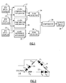
- Figure 1 is a block diagram of a three phase detection circuit according to the principles of the present invention;
- Figure 2 is a schematic diagram of the optically coupled input for the three phase detection circuit of the present invention;
- Figure 3 is a schematic circuit diagram of a three phase detection circuit according to the principles of the present invention;
- Figure 4 illustrates the operational wave forms of the illustrated embodiment shown in Figure 1 under conditions of proper phase rotation;
- Figure 5 illustrates operational wave forms of the illustrative embodiment shown in Figure 1 when the incoming three phase power is out-of-phase; and
- Figure 6 illustrates wave forms of out-of-phase sequence, in-phase sequence and reference level of the illustrative embodiment shown in Figure 1 over a wide range of frequencies.
- Referring to Figure 1, opto-
couplers integrators integrators integrators peak detector 24. Opto-coupler 21 also provides a signal to referenceintegrator 22 which integrates to a positive peak level which varies with incoming line frequency. The output of theintegrator 22 is fed topeak detector 26. The outputs of the twopeak detectors comparator 28 which compares the peak integrated amplitude of the input signals and provides an output signal if the incoming three phase power is out of phase. - Referring now to Figures 2 and 3 for details of specific circuits which may be utilized for the phase reversal detection of the present invention, the circuits shown therein are arranged to monitor three phase power sources and include separate opto-
couplers coupler 21 goes from the negative to the positive half cycle of the incoming sine wave, opto-coupler 21 is turned ON, which in turn turns ONtransistor 32 and forces the output of theintegrator 22 to integrate to a positive peak level or a high state, which is fed to peakdetector 26 which in turn has an output that is the input reference voltage forcomparator 28. When the incoming sine wave at opto-coupler 21 goesnegative integrator 22 is reset to a low state. - When the opto-
coupler 21 turns ON it also provides an input signal to comparator/integrator 27 (comprisingcomparator section 27a andintegrator section 27b) which forces the output of the comparator/integrator 27 to integrate to a positive potential if the opto-coupler 23 is off, and continued to integrate until opto-coupler 23 is turned ON which forces the reset of theintegrator section 27b of comparator/integrator 27 to a low state. - As the incoming sine wave signal at opto-
coupler 23 goes from the negative to the positive half cycle opto-coupler 23 turns ON which also provides an input signal to comparator/ integrator 20 (comprising comparator section 20a andintegrator section 20b) which integrates to a positive DC level or a high state if the opto-couple 25 is off, and continues to integrate until opto-coupler 25 turns ON which forces the output of theintegrator section 20b of comparator/integrator 20 to be reset to a low state. This positive peak level is fed topeak detector 24 which in turn provides a positive DC input signal tocomparator 28.Comparator 28 compares the outputs ofpeak detectors comparator 28 will be low and will holdtransistor 34 ofoutput switch 36 cut off. - If the incoming three phase power is out of phase the comparator/
integrators respective input resistors capacitors respective comparators 27a, 20a. These inputs will keep the comparator/integrators integrators comparator 28 from thepeak detector 24 will be at a higher potential then the input ofcomparator 28 frompeak detector 26 and thetransistor 34 of theoutput switch 36 will be turned ON and thephase reversal relay 46 will be energized. Upon energization of the phasereversal relay 46 two of the input phases can be reversed to an output device which puts the input phase sequence in proper phase. - The operational waveforms of the three phase detection circuit of Fig. 3, when the incoming three phase power is "in-phase" is illustrated in Fig. 4. As shown the incoming three phases are designated Phase A(ΦA), Phase B(ΦB), and Phase C(ΦC) respectively. When the incoming phases go from the negative to the positive half cycle of the respective incoming sine waves the respective opto-couplers are turned ON to produce
outputs integrators positive potential coupler 21 generates a square-wave and also forcesΦC reference integrator 22 to integrate to a higherpositive peak level 55 than either ΦA or ΦB comparator/integrator outputs. - Further, the operational wave forms of the three phase detection circuit, when the incoming three phase power is "out-of-phase" is illustrated in Fig. 5. As noted the comparator/
integrators positive potential output 58 of thereference integrator 22. - The
input 48 to thecomparator 28 from thepeak detector 26, and theinputs comparator 28 from thepeak detector 24 when the incoming power is "in-phase" and "out-of-phase", respectively, over a wide range of frequencies, is shown in Fig. 6. Thus, the present invention provides polyphase detection over a wide frequency range. - While the present invention has been described in detail with reference to the illustrative embodiment; many modifications and variations would present themselves to those skilled in the art, for example, optical couplers may be replaced with direct coupled switches with departing from the true spirit and scope of the invention.
Claims (3)
- A polyphase line signal reversal detection system characterized by:
at least first, second, and third input signal coupling means adapted to be coupled to the polyphase line signal for generating output waveforms indicative of the input signals;
a first integrating circuit means having an integrating means coupled to said first and second input signal coupling means and responsive to the respective output waveforms for generating a first peak integrated signal, said first peak integrated signal is initiated during the positive half cycle of the first output wave only when the second output waveform is in the negative half cycle and said first peak integrated signal is terminated when the second output waveform starts the positive half cycle;
a second integrating circuit means having an integrating means coupled to said second and third input signal coupling means and responsive to the respective output waveforms for generating a second peak integrated signal, said second peak integrated signal is initiated during the positive half cycle of the second output waveform only when the third output waveform is in the negative half cycle and said second peak integrated signal is terminated when the third output waveform starts the positive half cycle;
a reference integrating circuit means having an integrating means coupled to said first waveform coupling means and responsive to the first output for generating a reference integrated signal, said reference integrated signal is initiated at the start of the positive half cycle of the first output waveform and is terminated at the start of the negative half cycle of the first output waveform; and
a comparator circuit means for comparing said first peak integrated signal, said second integrated signal, and
said reference integrated signal, for providing an output indication signal of the phase sequence of the poly phase line signal. - A polyphase line signal reversal detection system as setforth in claim 1 further characterized by a switch means responsive to said output indication signal of said comparator circuit means for switching at least two of the phase sequences when the polyphase line signal is out of sequence.
- A polyphase line signal reversal detection system as setforth in claim 1 wherein said at least first, second, and third input signal coupling means includes an optical coupling means connected to respective phases of the polyphase line.
Applications Claiming Priority (2)
| Application Number | Priority Date | Filing Date | Title |
|---|---|---|---|
| US834748 | 1992-02-13 | ||
| US07/834,748 US5184063A (en) | 1992-02-13 | 1992-02-13 | Three phase reversal detection system |
Publications (2)
| Publication Number | Publication Date |
|---|---|
| EP0556147A2 true EP0556147A2 (en) | 1993-08-18 |
| EP0556147A3 EP0556147A3 (en) | 1995-04-12 |
Family
ID=25267704
Family Applications (1)
| Application Number | Title | Priority Date | Filing Date |
|---|---|---|---|
| EP93630012A Withdrawn EP0556147A3 (en) | 1992-02-13 | 1993-02-11 | Three phase reversal detection system |
Country Status (4)
| Country | Link |
|---|---|
| US (1) | US5184063A (en) |
| EP (1) | EP0556147A3 (en) |
| JP (1) | JPH05302942A (en) |
| CA (1) | CA2088640A1 (en) |
Families Citing this family (10)
| Publication number | Priority date | Publication date | Assignee | Title |
|---|---|---|---|---|
| US5039936A (en) * | 1989-12-13 | 1991-08-13 | Houston Industries Incorporated | Voltage rotation indicator mounting apparatus |
| JPH08289466A (en) * | 1995-04-17 | 1996-11-01 | Sanyo Electric Co Ltd | Erroneous wiring detector for power supply |
| US5652505A (en) * | 1995-12-18 | 1997-07-29 | Neilsen-Kuljian, Inc. | Power consumption measurement device for a multiphase alternating current system |
| US5796565A (en) * | 1996-12-02 | 1998-08-18 | Verkhovskiy; Yan | Apparatus and method for starting and protecting a three-phase motor |
| JP4107789B2 (en) * | 2000-08-10 | 2008-06-25 | 三洋電機株式会社 | Power supply reverse phase detection circuit |
| JP2007505327A (en) * | 2003-05-27 | 2007-03-08 | コニンクリユケ フィリップス エレクトロニクス エヌ.ブイ. | Phase detector and phase detection method |
| AU2008321378B2 (en) * | 2007-11-13 | 2012-04-12 | Emerson Climate Technologies, Inc. | Three-phase detection module |
| WO2009082395A1 (en) * | 2007-12-21 | 2009-07-02 | Carrier Corporation | Method and system for low-power three-phase detection |
| KR101614797B1 (en) * | 2008-09-22 | 2016-04-22 | 삼성전자 주식회사 | Device for protection of power factor correction in three phase power supply and control method thereof |
| CN102664568B (en) * | 2012-04-23 | 2014-12-24 | 库顿电子科技(上海)有限公司 | Novel solid-state relay aiming at running direction control of three-phase alternating current motor and method |
Citations (4)
| Publication number | Priority date | Publication date | Assignee | Title |
|---|---|---|---|---|
| US3825768A (en) * | 1973-02-15 | 1974-07-23 | Eaton Corp | Phase sequence and power loss detector |
| US4333119A (en) * | 1980-04-28 | 1982-06-01 | Purex Corporation | Power monitor system |
| US4636720A (en) * | 1984-11-30 | 1987-01-13 | Abex Corporation | Phase detector |
| US4802053A (en) * | 1987-03-11 | 1989-01-31 | Square D Company | Control circuitry including phase failure relay |
Family Cites Families (5)
| Publication number | Priority date | Publication date | Assignee | Title |
|---|---|---|---|---|
| US3848160A (en) * | 1973-05-21 | 1974-11-12 | Gen Electric Canada | Circuit for detecting phase unbalance in a three phase supply |
| US4121271A (en) * | 1973-12-26 | 1978-10-17 | General Electric Company | Reverse power flow detector and control circuit |
| US3976919A (en) * | 1975-06-04 | 1976-08-24 | Borg-Warner Corporation | Phase sequence detector for three-phase AC power system |
| US3999087A (en) * | 1975-08-15 | 1976-12-21 | Westinghouse Electric Corporation | Missing phase detection circuit for use with three-phase power sources |
| JPS5547459A (en) * | 1978-09-30 | 1980-04-03 | Fanuc Ltd | Dc motor driving reverse and missing phase detector circuit |
-
1992
- 1992-02-13 US US07/834,748 patent/US5184063A/en not_active Expired - Fee Related
-
1993
- 1993-02-02 CA CA002088640A patent/CA2088640A1/en not_active Abandoned
- 1993-02-10 JP JP5022201A patent/JPH05302942A/en active Pending
- 1993-02-11 EP EP93630012A patent/EP0556147A3/en not_active Withdrawn
Patent Citations (4)
| Publication number | Priority date | Publication date | Assignee | Title |
|---|---|---|---|---|
| US3825768A (en) * | 1973-02-15 | 1974-07-23 | Eaton Corp | Phase sequence and power loss detector |
| US4333119A (en) * | 1980-04-28 | 1982-06-01 | Purex Corporation | Power monitor system |
| US4636720A (en) * | 1984-11-30 | 1987-01-13 | Abex Corporation | Phase detector |
| US4802053A (en) * | 1987-03-11 | 1989-01-31 | Square D Company | Control circuitry including phase failure relay |
Non-Patent Citations (1)
| Title |
|---|
| IBM TECHNICAL DISCLOSURE BULLETIN, vol.19, no.11, April 1977 pages 4297 - 4298 K.R.WILLIAMS 'Primary power phase monitor' * |
Also Published As
| Publication number | Publication date |
|---|---|
| CA2088640A1 (en) | 1993-08-14 |
| US5184063A (en) | 1993-02-02 |
| EP0556147A3 (en) | 1995-04-12 |
| JPH05302942A (en) | 1993-11-16 |
Similar Documents
| Publication | Publication Date | Title |
|---|---|---|
| US4631536A (en) | Multiplex submersible pump telemetry system | |
| US4658241A (en) | Surveillance system including transmitter and receiver synchronized by power line zero crossings | |
| US5184063A (en) | Three phase reversal detection system | |
| US4780656A (en) | Drive and protection system for variable speed motor | |
| US5442278A (en) | Apparatus for detecting the frequency of an input signal by counting pulses during an input signal cycle | |
| US5959858A (en) | Electric power conversion apparatus | |
| EP0372240A3 (en) | Zero voltage crossover detector for polyphase systems | |
| EP1380096B1 (en) | Control means and method for a resonant transistor halfbridge with critical conduction mode | |
| EP0479525A2 (en) | Absolute position measuring resolver apparatus with backup means in power failure | |
| US4066959A (en) | Electronic volt-square-hour metering method and apparatus | |
| JPH01107663A (en) | Method and apparatus for determining extinction angle of valve of inverter | |
| RU2014707C1 (en) | Equipment for automatic synchronization of synchronous generators | |
| SU1308908A1 (en) | Device for comparing amplitudes of two low-frequency harmonic voltages | |
| US4351194A (en) | Gyro autophase system | |
| RU1814138C (en) | Protected self-contained three-phase network | |
| GB2047024A (en) | Commutating capacitor charge detection circuit and method | |
| JP3060400B2 (en) | Inverter monitoring device | |
| SU1302416A1 (en) | Frequency regulator of d.c.voltage-to-a.c.voltage electric machine converter | |
| JPS6227037Y2 (en) | ||
| JPS61210967A (en) | Phase detecting circuit for three-phase ac | |
| SU1381671A1 (en) | Two-cycle transistor converter | |
| JP2648604B2 (en) | Open phase detector | |
| SU1038960A1 (en) | Signal receiving device | |
| SU546925A1 (en) | Device for monitoring resolver sensors | |
| SU864000A1 (en) | Angular displacement-to-voltage cinverter |
Legal Events
| Date | Code | Title | Description |
|---|---|---|---|
| PUAI | Public reference made under article 153(3) epc to a published international application that has entered the european phase |
Free format text: ORIGINAL CODE: 0009012 |
|
| AK | Designated contracting states |
Kind code of ref document: A2 Designated state(s): DE ES FR GB IT |
|
| PUAL | Search report despatched |
Free format text: ORIGINAL CODE: 0009013 |
|
| AK | Designated contracting states |
Kind code of ref document: A3 Designated state(s): DE ES FR GB IT |
|
| 17P | Request for examination filed |
Effective date: 19951002 |
|
| 17Q | First examination report despatched |
Effective date: 19960918 |
|
| STAA | Information on the status of an ep patent application or granted ep patent |
Free format text: STATUS: THE APPLICATION IS DEEMED TO BE WITHDRAWN |
|
| 18D | Application deemed to be withdrawn |
Effective date: 19970129 |