EP0552005B1 - Method and apparatus for noise burst detection in a signal processor - Google Patents
Method and apparatus for noise burst detection in a signal processor Download PDFInfo
- Publication number
- EP0552005B1 EP0552005B1 EP93300144A EP93300144A EP0552005B1 EP 0552005 B1 EP0552005 B1 EP 0552005B1 EP 93300144 A EP93300144 A EP 93300144A EP 93300144 A EP93300144 A EP 93300144A EP 0552005 B1 EP0552005 B1 EP 0552005B1
- Authority
- EP
- European Patent Office
- Prior art keywords
- signal
- noise
- providing
- adpcm
- total energy
- Prior art date
- Legal status (The legal status is an assumption and is not a legal conclusion. Google has not performed a legal analysis and makes no representation as to the accuracy of the status listed.)
- Expired - Lifetime
Links
Images
Classifications
-
- H—ELECTRICITY
- H04—ELECTRIC COMMUNICATION TECHNIQUE
- H04M—TELEPHONIC COMMUNICATION
- H04M1/00—Substation equipment, e.g. for use by subscribers
- H04M1/72—Mobile telephones; Cordless telephones, i.e. devices for establishing wireless links to base stations without route selection
- H04M1/725—Cordless telephones
- H04M1/72502—Cordless telephones with one base station connected to a single line
-
- H—ELECTRICITY
- H04—ELECTRIC COMMUNICATION TECHNIQUE
- H04B—TRANSMISSION
- H04B1/00—Details of transmission systems, not covered by a single one of groups H04B3/00 - H04B13/00; Details of transmission systems not characterised by the medium used for transmission
- H04B1/06—Receivers
- H04B1/10—Means associated with receiver for limiting or suppressing noise or interference
- H04B1/1027—Means associated with receiver for limiting or suppressing noise or interference assessing signal quality or detecting noise/interference for the received signal
-
- H—ELECTRICITY
- H04—ELECTRIC COMMUNICATION TECHNIQUE
- H04B—TRANSMISSION
- H04B14/00—Transmission systems not characterised by the medium used for transmission
- H04B14/02—Transmission systems not characterised by the medium used for transmission characterised by the use of pulse modulation
- H04B14/06—Transmission systems not characterised by the medium used for transmission characterised by the use of pulse modulation using differential modulation, e.g. delta modulation
- H04B14/066—Transmission systems not characterised by the medium used for transmission characterised by the use of pulse modulation using differential modulation, e.g. delta modulation using differential modulation with several bits [NDPCM]
- H04B14/068—Transmission systems not characterised by the medium used for transmission characterised by the use of pulse modulation using differential modulation, e.g. delta modulation using differential modulation with several bits [NDPCM] with adaptive feedback
-
- H—ELECTRICITY
- H04—ELECTRIC COMMUNICATION TECHNIQUE
- H04M—TELEPHONIC COMMUNICATION
- H04M1/00—Substation equipment, e.g. for use by subscribers
- H04M1/72—Mobile telephones; Cordless telephones, i.e. devices for establishing wireless links to base stations without route selection
- H04M1/725—Cordless telephones
- H04M1/72502—Cordless telephones with one base station connected to a single line
- H04M1/72505—Radio link set-up procedures
Definitions
- This invention relates generally to signal processors, and more particularly, to signal processors with noise burst detection and related methods.
- a digital cordless telephone handset receives an analog speech signal via a microphone, converts the analog speech signal into a digital speech signal, compresses the digital speech signal, modulates the compressed signal at a radio frequency (RF), and transmits the modulated RF signal through an antenna.
- the transmitted RF signal is received by a nearby base station where it may be converted to an analog signal (or remain in digital form for digital switching equipment), and ultimately relayed to the destination telephone.
- the telephone signal undergoes the same process in reverse.
- the base station transmits a digital RF signal to the handset which is received via the antenna, demodulated, decompressed, and converted into an analog speech signal which drives a speaker in the handset.
- CT-2 One standard for the operation of a cordless telephone handset is the U.K. Cordless Telephone, Second Generation (CT-2) standard.
- a CT-2 handset receives an analog voice signal from a microphone.
- the voice signal is converted to digital pulse code modulation (PCM) format, processed through an adaptive differential pulse code modulation (ADPCM) encoder, and then modulated and transmitted according to the CT-2 Common Air Interface (CAI) protocol to a base station.
- PCM digital pulse code modulation
- ADPCM adaptive differential pulse code modulation
- CAI Common Air Interface
- CT-2 specifies CCITT G.721 ADPCM for the operation of the ADPCM encoder. Transmit and receive signals are sent and received to and from the base station in packets in a ping-pong fashion.
- CAI specifies that a part of the packet includes signalling information including such things as call setup and termination requests and handshaking information.
- a packet is received, demodulated, processed through a G.721 ADPCM decoder, converted from digital PC
- Both analog and digital functions are necessary in the operation of a digital cordless telephone handset.
- a conventional integrated circuit such as the Motorola MC145554 m-law PCM Codec-Filter or the Motorola MC145557 A-law PCM Codec-Filter may be used.
- a conventional integrated circuit such as the Motorola MC145532 ADPCM Transcoder may be used. Both of these functions may also be combined into a single, mixed signal processing integrated circuit.
- the handset establishes a digital link with the base station.
- the link is normally maintained until the call is completed.
- the link may be lost or broken between the handset and the base station during the call. For example, if the user moves the handset outside of the range of the base station, then the link may be lost.
- a noise level of about 3 to 6 decibels (dB) below the maximum level may occur.
- the only method specified by the CAI protocol to detect link loss is to detect the absence of an expected handshake message in the signalling part of the packet.
- Intervals in the transmission of handshake messages may be as long as several seconds.
- One way to lessen the detection time is to force periodic communication between the base station and the handset, which results in a reduction in detection time to several hundred milliseconds. Even then, a user may hear a loud noise when the link is broken.
- U.S. Patent No. 4,811,404 discloses a noise suppression system in which an input speech signal is broken into a plurality of frequency channels.
- the signal-to-noise ratio (SNR) within each of the channels is estimated, and the signal is attenuated on a per-channel basis according to the estimated SNR.
- the SNR is estimated by dividing the current energy estimate by the current background noise estimate from the previous frame.
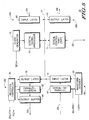
- FIG. 1 illustrates in block diagram form a telephone handset including an ADPCM CODEC.
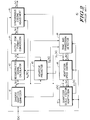
- FIG. 2 illustrates in block form a functional block diagram of a prior art ADPCM decoder conforming to CCITT Recommendation G.721 or G.726.
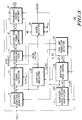
- FIG. 3 illustrates in block form a functional block diagram of the ADPCM decoder of FIG. 1 in accordance with the present invention.
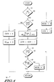
- FIG. 4 illustrates a flow chart in accordance with and illustrating the method of the present invention.
- FIG. 5 illustrates in block form the ADPCM transcoder of FIG. 1 in accordance with a preferred embodiment of the present invention.
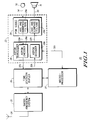
- FIG. 1 illustrates in block diagram form a CT-2 telephone handset 20 including an ADPCM CODEC 22.
- Handset 20 conforms to the CT-2 standard.
- telephone signals are received and transmitted digitally in packets in a half-duplex or ping-pong scheme between handset 20 and a base station (not shown in FIG. 1).
- An antenna 24 is used for transmitting and receiving radio-frequency (RF) representations of telephonic signals.
- An RF system 25 is connected to antenna 24 for receiving and demodulating, and modulating and transmitting, digital streams of telephonic data.
- signal refers to a time-varying electrical signal
- digital signal refers to a series of digital samples of the signal.
- a "packet" includes a portion of the digital signal, or alternatively, a specified number of digital samples of the telephone signal, along with digital signalling bits.
- a microphone 30 provides an analog telephone signal via input signal lines 34 to ADPCM CODEC 22.
- ADPCM CODEC 22 is a single integrated circuit incorporating both an ADPCM transcoder 28 and a PCM codec 29.
- PCM codec 29 performs the function of a conventional integrated circuit, such as the Motorola MC145554 m-law PCM Codec-Filter or the Motorola MC145557 A-law PCM Codec-Filter.
- PCM codec 29 includes two portions, an analog-to-digital converter (ADC) and bandpass filters 29a, and a digital-to-analog converter (DAC) and lowpass filters 29b.
- ADC analog-to-digital converter
- DAC digital-to-analog converter
- ADC and bandpass filters 29a converts the analog telephone signal to a digital telephone signal and converts it to PCM according to the A-law or m-law algorithm, and provides the digital telephone signal to ADPCM transcoder 28 via input signals 33a.
- ADPCM transcoder 28 includes two portions, an ADPCM encoder 28a, and an ADPCM decoder 28b.
- ADPCM encoder 28a in turn compresses the 64 kbps digital telephone signal to a 32 kbps ADPCM signal according to the G.721 standard and provides the ADPCM signal to time division duplex block 26 via a signal line 32a.
- Time division duplex block 26 then combines signalling bits from microprocessor 27 with the compressed digital data from ADPCM transcoder 28 to form a CT-2 packet.
- Time division duplex block 26 provides the CT-2 packet to radio frequency system 25, which modulates it and provides it as an RF signal to antenna 24, where it is radiated and eventually received by the base station.
- the modulation scheme is a two-level FSK shaped by an approximately Gaussian filter, as described in the CT-2 CAI Specification.
- a packet from the base station is received as a modulated RF signal on antenna 24.
- Radio frequency system 25 receives the RF signal and demodulates it.
- the packet is then presented to a time division duplex block 26.
- Time division duplex block 26 splits the packet into its two constituent components, making signalling bits available to microprocessor 27.
- Time division duplex block 26 makes the compressed digital signal available to an ADPCM transcoder 28 via signals 32b.
- microprocessor 27 reads the signalling bits and performs associated signalling functions, such as call setup and disconnect.
- ADPCM decoder 28b decompresses the compressed digital signal received from time division duplex block 26.
- ADPCM decoder 28b conforms to CCITT Recommendation G.721.
- ADPCM decoder 28b converts the 32 kbps ADPCM digital signal to 64 kbps PCM according to standard G.721 ADPCM.
- ADPCM transcoder 28 is connected via input and output signals 32c to microprocessor 27, which initializes and controls the operation thereof.
- DAC and lowpass filters 29b receives the PCM data via input signals 33b, performs A-law or m-law decompression and digital-to-analog conversion to form an analog telephone signal, and provides theanalog telephone signal to a speaker 31 and a ringer (not shown in FIG. 1) via output signals 35.
- One possibility for detecting a broken link is to compare the average energy level of the received signal to a threshold. If the average energy level over a predetermined period exceeds the threshold, then it is possible to conclude that the link has been broken and to mute the output to speaker 31.
- microprocessor 27 To calculate average power with this method, microprocessor 27 must sample the received digital PCM data conducted on signal 33b. For some systems, however, this calculation is impractical. First, PCM is a logarithmic format; to calculate power, the data must be converted to a linear format. Second, in implementations in which ADPCM transcoder 28 and PCM codec 29 are included in a single integrated circuit (such as mixed signal processing system 22), signal 33b is not available externally without dedicating additional device pins (for data, clock, and enable signals). Third, some applications, such as the CT-2 handset itself, are extremely cost-sensitive; to minimize cost, microprocessor 27 may have reduced performance and may not have enough computational power to perform the power calculation.
- FIG. 2 illustrates in block form a functional block diagram of a prior art ADPCM decoder 40 conforming to CCITT Recommendation G.721 or G.726.
- ADPCM decoder 40 includes an inverse adaptive quantizer 41, a reconstructed signal calculator 42, an adaptive predictor 43, an output PCM format conversion 45, a synchronous coding adjustment 46, a quantizer scale factor adaptation 47, an adaptation speed control 48, and a tone and transition detector 49.
- the operation of each of these functional blocks is well-known and is described in CCITT Recommendation G.726-1990.
- FIG. 3 illustrates in block form a functional block diagram of ADPCM decoder 28b of FIG. 1 in accordance with the present invention.
- ADPCM decoder 28b includes a digital receive gain 44 and a noise detector 50. While preferred for ADPCM decoder 28b, other embodiments of the present invention may omit digital , receive gain 44. All other blocks besides perform similarly to corresponding blocks of the ADPCM decoder specified in G.721 or G.726 and shown in FIG. 2.
- Digital receive gain 44 receives the reconstructed signal s r (k) and a variable GAIN FACTOR. In response, digital receive gain 44 provides a reconstructed signal with gain labelled "s g (k)", and a signal labelled SYNC DISABLE to synchronous coding adjustment 46. Thus, digital receive gain 44 allows a linear gain adjustment.
- Noise detector 50 receives the reconstructed signal s r (k) and three parameters: a number of samples which will be included in the energy computation labelled "N", an energy threshold value labelled “NE TH ", and a noise detection enable labelled "ND”.
- Microprocessor 27 provides parameters N, NE TH , and ND to ADPCM transcoder 28 via a conventional serial communications port (SCP) of ADPCM transcoder 28 (not shown in FIG. 3).
- Noise detector 50 provides a noise indication labelled "NOISE” in response to the average energy of s r (k), labelled “E AVE ", exceeding predetermined threshold, labelled "E TH ".
- An application-specific DSP includes a reduced number of instructions to optimize the operation for real-time signal processing applications.
- a divide instruction is not required for G.721 ADPCM. Thus, in order to minimize the number of instructions, it is desirable to eliminate the need for a divide instruction in the average power calculation.
- Average power calculation without a divide instruction can be done if the total energy, instead of the average energy, iscomputed.
- Noise detector 50 solves this problem by activating NOISE if the energy over N samples, labelled "NE AVE ", exceeds NE TH .
- microprocessor 27 In response to the activation of NOISE, microprocessor 27 attenuates or mutes the received signal. The muting may occur in ADPCM decoder 28, PCM codec 29, or directly to signal 35 provided to speaker 31. In the preferred embodiment, digital receive gain 44 allows microprocessor 27 to mute the received signal digitally by setting GAIN FACTOR to zero.
- FIG. 4 illustrates a flow chart in accordance with and illustrating the method of the present invention.
- the flow chart of FIG. 4 implements noise detector 50 of FIG. 3, and is assigned the same reference number.
- ADPCM decoder 28b starts execution of the noise detection routine by checking, at step 51, whether a noise detection control bit, labelled "ND", is set. If ND is not set, then noise detector 50 is disabled and program flow is returned to a main routine after NOISE is cleared at step 52 and CNTR is set to negative 1 at step 61. If ND is set, then a counter variable labelled "CNTR" is checked at step 53.
- CNTR is an internal variable that keeps track of how many values of
- CNTR On the following sample, a positive value of CNTR is detected at step 53.
- NE AVE represents an estimate of the total energy for the time interval defined by the sample interval times N. For G.721 32 kbps ADPCM, the sample interval is 125 microseconds ( ⁇ sec), and thus NE AVE represents an estimate of the total energy in the signal over an (N)*(125 ⁇ sec) interval.
- NE AVE is compared to NE TH at step 59. If NE AVE is not less than NE TH , then NOISE is set at step 60.
- the flow chart of FIG. 4 illustrates a decrementing sample counter. It is also possible to initialize an incrementing sample counter to zero and then to compare the value of NE AVE to NE TH when the counter reaches N. Also, NOISE was set in response to a false result of a test whether NE AVE is less than NE TH at step 59. In another embodiment, NOISE could be set in response to a true result of a test of whether NE AVE is greater than NE TH .
- FIG. 5 illustrates in block form ADPCM transcoder 28 of FIG. 1 in accordance with a preferred embodiment of the present invention. It should be noted that FIG. 5 depicts ADPCM transcoder 28 according to functional blocks representative of hardware circuitry. By contrast, FIG. 3 illustrates a functional block diagram of ADPCM decoder 28b. FIG. 5 clarifies how the blocks of ADPCM transcoder 28 perform the functions illustrated by FIG. 3. In FIG. 5, blocks which correspond to the encoder function are referred to as 28a', and blocks which correspond to the decoder function are labelled 28b', with the remaining blocks performing parts of both functions.
- ADPCM transcoder 28 includes a digital signal processor (DSP) 70.
- DSP 70 is coupled to a communications bus 73 for receiving data therefrom and providing data thereto.
- a clock generator 72 receives a signal labelled "SPC" which is the output of a crystal oscillator (not shown).
- Clock generator 72 is coupled to DSP 70 and provides a clock signal thereto.
- a serial control port (SCP) 71 is also connected to communications bus 73.
- SCP 71 is connected to microprocessor 27 of FIG. 1 via signal lines 32c.
- SCP 71 allows microprocessor 27 to initialize and control the operation of ADPCM transcoder 28.
- SCP 71 includes registers which store ND, N, NE TH , and GAIN FACTOR from microprocessor 27, and NOISE from ADPCM decoder 28b.
- ADPCM encoder 28a' includes an input latch 80, an output latch 81, a parallel-to-serial block 82, an output buffer 84, and a register controller 85.
- Input latch 80 is connected to PCM codec 29 of FIG. 1 via input signal lines 33a.
- Input latch 80 latches digital PCM data words from PCM codec 29 and provides the data to DSP 70 via communications bus 73.
- DSP 70 performs the function of a G.721 ADPCM encoder through microcode.
- DSP 70 also provides ADPCM data words via communications bus 73 to output latch 81.
- the ADPCM data word may be either 8, 4, 3, or 2 bits corresponding to a data rate of either 64, 32, 24, or 16 kbps, respectively.
- Parallel-to-serial block 82 is connected to output latch 81 and provides an ADPCM data word serially to output buffer 84, which provides the data to time division duplex block 26 via signal line 32a.
- Register controller 85 is connected to, and controls the operation of, output latch 81, parallel-to-serial block 82, and output buffer 84 in response to a clock input signal labelled "BCLKT" and a control signal labelled "FST".
- ADPCM decoder 28b includes a serial-to-parallel block 90, an input latch 91, a waveform decoder 92, and an output latch 93.
- Serial-to-parallel block 90 receives an ADPCM-encoded stream of data bits via input signal line 32b, combines the data into ADPCM data words, and provides the data words to input latch 91.
- Input latch 91 stores an ADPCM data word and makes it available to DSP 70.
- Waveform decoder 92 receives input signals labelled "FSR" and "BCLKR". Signal BCLKR clocks the received data, and signal FSR determines the operating mode. Together, signals BCLKR and FSR determine operation at a data rate of either 64, 32, 24, or 16 kbps.
- DSP 70 performs the function of a G.721 ADPCM decoder having the digital receive gain and noise detection functions illustrated in FIG. 3 in microcode. DSP 70 provides digital PCM signal s d (k) to output latch 93, which subsequently provides it to PCM codec 29 via signal line 33b.
- ADPCM transcoder 28 performs the functions of a G.721 ADPCM encoder and a G.721 ADPCM decoder.
- FIG. 5 several blocks of integrated circuit hardware assist DSP 70 in performing each function.
- Microcode running on DSP 70 actually performs the functional block diagram of FIG. 3, and thus DSP 70 is common to both the ADPCM encoder and decoder functions.
- some or all of the functional blocks of FIG. 3 may be performed by hardware circuitry.
- digital receive gain 44 provides a convenient method of muting the received signal after detection of a noise burst or broken link, other methods of attenuating the received signal are possible. Accordingly, it is intended by the appended claims to cover all modifications of the invention which fall within the scope of the invention.
Description
- This invention relates generally to signal processors, and more particularly, to signal processors with noise burst detection and related methods.
- The increased density and reduced cost of integrated circuit components has made many previously impractical products commercially viable. One type of product made viable by advances in integrated circuit technology is the digital cordless telephone. A digital cordless telephone handset receives an analog speech signal via a microphone, converts the analog speech signal into a digital speech signal, compresses the digital speech signal, modulates the compressed signal at a radio frequency (RF), and transmits the modulated RF signal through an antenna. The transmitted RF signal is received by a nearby base station where it may be converted to an analog signal (or remain in digital form for digital switching equipment), and ultimately relayed to the destination telephone. When a similar signal is received from the destination telephone, the telephone signal undergoes the same process in reverse. The base station transmits a digital RF signal to the handset which is received via the antenna, demodulated, decompressed, and converted into an analog speech signal which drives a speaker in the handset.
- One standard for the operation of a cordless telephone handset is the U.K. Cordless Telephone, Second Generation (CT-2) standard. A CT-2 handset receives an analog voice signal from a microphone. The voice signal is converted to digital pulse code modulation (PCM) format, processed through an adaptive differential pulse code modulation (ADPCM) encoder, and then modulated and transmitted according to the CT-2 Common Air Interface (CAI) protocol to a base station. CT-2 specifies CCITT G.721 ADPCM for the operation of the ADPCM encoder. Transmit and receive signals are sent and received to and from the base station in packets in a ping-pong fashion. CAI specifies that a part of the packet includes signalling information including such things as call setup and termination requests and handshaking information. For signal reception, a packet is received, demodulated, processed through a G.721 ADPCM decoder, converted from digital PCM to analog, and then provided to a speaker.
- Both analog and digital functions are necessary in the operation of a digital cordless telephone handset. To perform the conversion from analog to PCM and from PCM to analog, a conventional integrated circuit such as the Motorola MC145554 m-law PCM Codec-Filter or the Motorola MC145557 A-law PCM Codec-Filter may be used. To perform the conversion from PCM to ADPCM and from ADPCM to PCM, a conventional integrated circuit such as the Motorola MC145532 ADPCM Transcoder may be used. Both of these functions may also be combined into a single, mixed signal processing integrated circuit.
- In the CT-2 cordless telephone system, the handset establishes a digital link with the base station. The link is normally maintained until the call is completed. In some cases, the link may be lost or broken between the handset and the base station during the call. For example, if the user moves the handset outside of the range of the base station, then the link may be lost. The result is that a high level of white noise is provided to the speaker due to the randomness of the received data until the broken link is detected and the noise is muted. A noise level of about 3 to 6 decibels (dB) below the maximum level may occur. The only method specified by the CAI protocol to detect link loss is to detect the absence of an expected handshake message in the signalling part of the packet. Intervals in the transmission of handshake messages may be as long as several seconds. One way to lessen the detection time is to force periodic communication between the base station and the handset, which results in a reduction in detection time to several hundred milliseconds. Even then, a user may hear a loud noise when the link is broken.
- U.S. Patent No. 4,811,404 discloses a noise suppression system in which an input speech signal is broken into a plurality of frequency channels. The signal-to-noise ratio (SNR) within each of the channels is estimated, and the signal is attenuated on a per-channel basis according to the estimated SNR. The SNR is estimated by dividing the current energy estimate by the current background noise estimate from the previous frame.
- Accordingly, there is provided, in one form, a method for noise burst detection in a signal processor as claimed in
claim 1. - In another form, there is provided a signal processor with noise burst detection as claimed in claim 9.
- These and other features and advantages will be more clearly understood from the following detailed description taken in conjunction with the accompanying drawings.
- FIG. 1 illustrates in block diagram form a telephone handset including an ADPCM CODEC.
- FIG. 2 illustrates in block form a functional block diagram of a prior art ADPCM decoder conforming to CCITT Recommendation G.721 or G.726.
- FIG. 3 illustrates in block form a functional block diagram of the ADPCM decoder of FIG. 1 in accordance with the present invention.
- FIG. 4 illustrates a flow chart in accordance with and illustrating the method of the present invention.
- FIG. 5 illustrates in block form the ADPCM transcoder of FIG. 1 in accordance with a preferred embodiment of the present invention.
- FIG. 1 illustrates in block diagram form a CT-2
telephone handset 20 including an ADPCMCODEC 22.Handset 20 conforms to the CT-2 standard. According to the CT-2 protocol, telephone signals are received and transmitted digitally in packets in a half-duplex or ping-pong scheme betweenhandset 20 and a base station (not shown in FIG. 1). Anantenna 24 is used for transmitting and receiving radio-frequency (RF) representations of telephonic signals. AnRF system 25 is connected toantenna 24 for receiving and demodulating, and modulating and transmitting, digital streams of telephonic data. As used here, the term "signal" refers to a time-varying electrical signal, and the term "digital signal" refers to a series of digital samples of the signal. A "packet" includes a portion of the digital signal, or alternatively, a specified number of digital samples of the telephone signal, along with digital signalling bits. - A
microphone 30 provides an analog telephone signal viainput signal lines 34 to ADPCM CODEC 22. In the illustrated embodiment, ADPCM CODEC 22 is a single integrated circuit incorporating both anADPCM transcoder 28 and aPCM codec 29.PCM codec 29 performs the function of a conventional integrated circuit, such as the Motorola MC145554 m-law PCM Codec-Filter or the Motorola MC145557 A-law PCM Codec-Filter. Functionally,PCM codec 29 includes two portions, an analog-to-digital converter (ADC) andbandpass filters 29a, and a digital-to-analog converter (DAC) andlowpass filters 29b. ADC andbandpass filters 29a converts the analog telephone signal to a digital telephone signal and converts it to PCM according to the A-law or m-law algorithm, and provides the digital telephone signal toADPCM transcoder 28 viainput signals 33a. Functionally,ADPCM transcoder 28 includes two portions, anADPCM encoder 28a, and anADPCM decoder 28b. ADPCMencoder 28a in turn compresses the 64 kbps digital telephone signal to a 32 kbps ADPCM signal according to the G.721 standard and provides the ADPCM signal to timedivision duplex block 26 via asignal line 32a. Timedivision duplex block 26 then combines signalling bits frommicroprocessor 27 with the compressed digital data fromADPCM transcoder 28 to form a CT-2 packet. Timedivision duplex block 26 provides the CT-2 packet toradio frequency system 25, which modulates it and provides it as an RF signal toantenna 24, where it is radiated and eventually received by the base station. The modulation scheme is a two-level FSK shaped by an approximately Gaussian filter, as described in the CT-2 CAI Specification. - For reception, a packet from the base station is received as a modulated RF signal on
antenna 24.Radio frequency system 25 receives the RF signal and demodulates it. The packet is then presented to a timedivision duplex block 26. Timedivision duplex block 26 splits the packet into its two constituent components, making signalling bits available tomicroprocessor 27. Timedivision duplex block 26 makes the compressed digital signal available to anADPCM transcoder 28 viasignals 32b. Subsequently,microprocessor 27 reads the signalling bits and performs associated signalling functions, such as call setup and disconnect. -
ADPCM decoder 28b decompresses the compressed digital signal received from timedivision duplex block 26. In the illustrated embodiment, as part of a CT-2 handset,ADPCM decoder 28b conforms to CCITT Recommendation G.721.ADPCM decoder 28b converts the 32 kbps ADPCM digital signal to 64 kbps PCM according to standard G.721 ADPCM.ADPCM transcoder 28 is connected via input andoutput signals 32c tomicroprocessor 27, which initializes and controls the operation thereof. DAC andlowpass filters 29b receives the PCM data via input signals 33b, performs A-law or m-law decompression and digital-to-analog conversion to form an analog telephone signal, and provides theanalog telephone signal to aspeaker 31 and a ringer (not shown in FIG. 1) via output signals 35. - One possibility for detecting a broken link is to compare the average energy level of the received signal to a threshold. If the average energy level over a predetermined period exceeds the threshold, then it is possible to conclude that the link has been broken and to mute the output to
speaker 31. - To calculate average power with this method,
microprocessor 27 must sample the received digital PCM data conducted onsignal 33b. For some systems, however, this calculation is impractical. First, PCM is a logarithmic format; to calculate power, the data must be converted to a linear format. Second, in implementations in whichADPCM transcoder 28 andPCM codec 29 are included in a single integrated circuit (such as mixed signal processing system 22),signal 33b is not available externally without dedicating additional device pins (for data, clock, and enable signals). Third, some applications, such as the CT-2 handset itself, are extremely cost-sensitive; to minimize cost,microprocessor 27 may have reduced performance and may not have enough computational power to perform the power calculation. - FIG. 2 illustrates in block form a functional block diagram of a prior
art ADPCM decoder 40 conforming to CCITT Recommendation G.721 or G.726.ADPCM decoder 40 includes an inverseadaptive quantizer 41, areconstructed signal calculator 42, anadaptive predictor 43, an outputPCM format conversion 45, asynchronous coding adjustment 46, a quantizerscale factor adaptation 47, anadaptation speed control 48, and a tone andtransition detector 49. The operation of each of these functional blocks is well-known and is described in CCITT Recommendation G.726-1990. - FIG. 3 illustrates in block form a functional block diagram of
ADPCM decoder 28b of FIG. 1 in accordance with the present invention.ADPCM decoder 28b includes a digital receivegain 44 and anoise detector 50. While preferred forADPCM decoder 28b, other embodiments of the present invention may omit digital , receivegain 44. All other blocks besides perform similarly to corresponding blocks of the ADPCM decoder specified in G.721 or G.726 and shown in FIG. 2. Digital receivegain 44 receives the reconstructed signal sr(k) and a variable GAIN FACTOR. In response, digital receivegain 44 provides a reconstructed signal with gain labelled "sg(k)", and a signal labelled SYNC DISABLE tosynchronous coding adjustment 46. Thus, digital receivegain 44 allows a linear gain adjustment. -
Noise detector 50 receives the reconstructed signal sr(k) and three parameters: a number of samples which will be included in the energy computation labelled "N", an energy threshold value labelled "NETH", and a noise detection enable labelled "ND".Microprocessor 27 provides parameters N, NETH, and ND toADPCM transcoder 28 via a conventional serial communications port (SCP) of ADPCM transcoder 28 (not shown in FIG. 3).Noise detector 50 provides a noise indication labelled "NOISE" in response to the average energy of sr(k), labelled "EAVE", exceeding predetermined threshold, labelled "ETH". One way of performing this energy calculation is to approximate EAVE by adding the absolute value of signal sr(k) over N sample periods, and then divide the result by N, which is expressed as:
- Average power calculation without a divide instruction can be done if the total energy, instead of the average energy, iscomputed.
Noise detector 50 solves this problem by activating NOISE if the energy over N samples, labelled "NEAVE", exceeds NETH. This formula is expressed mathematically as:
Microprocessor 27 of FIG. 1 provides NETH tonoise detector 50, which performs the average energy estimation of equation 2 and provides NOISE accordingly. In response to the activation of NOISE,microprocessor 27 attenuates or mutes the received signal. The muting may occur inADPCM decoder 28,PCM codec 29, or directly to signal 35 provided tospeaker 31. In the preferred embodiment, digital receivegain 44 allowsmicroprocessor 27 to mute the received signal digitally by setting GAIN FACTOR to zero. - FIG. 4 illustrates a flow chart in accordance with and illustrating the method of the present invention. The flow chart of FIG. 4 implements
noise detector 50 of FIG. 3, and is assigned the same reference number.ADPCM decoder 28b starts execution of the noise detection routine by checking, atstep 51, whether a noise detection control bit, labelled "ND", is set. If ND is not set, thennoise detector 50 is disabled and program flow is returned to a main routine after NOISE is cleared atstep 52 and CNTR is set to negative 1 atstep 61. If ND is set, then a counter variable labelled "CNTR" is checked atstep 53. CNTR is an internal variable that keeps track of how many values of |sr(k)| remain to be accumulated. CNTR is set to negative 1 upon power-up and reset ofADPCM codec 22. If ND = 1 (enabled), and CNTR is negative, then CNTR is initialized to N, the number of samples of |sr(k)| that will be used in the energy calculation, atstep 54. Internal variable NEAVE, which represents the total energy estimate over N samples, is initialized to zero atstep 55. - On the following sample, a positive value of CNTR is detected at
step 53. |sr(k)| is added to the value of NEAVE atstep 56, and CNTR is decremented atstep 57. CNTR is again tested atstep 58 to determine if it is negative.Steps step 59. If NEAVE is not less than NETH, then NOISE is set at step 60. - Different ways of implementing the algorithm are also possible. The flow chart of FIG. 4 illustrates a decrementing sample counter. It is also possible to initialize an incrementing sample counter to zero and then to compare the value of NEAVE to NETH when the counter reaches N. Also, NOISE was set in response to a false result of a test whether NEAVE is less than NETH at
step 59. In another embodiment, NOISE could be set in response to a true result of a test of whether NEAVE is greater than NETH. - FIG. 5 illustrates in block
form ADPCM transcoder 28 of FIG. 1 in accordance with a preferred embodiment of the present invention. It should be noted that FIG. 5 depictsADPCM transcoder 28 according to functional blocks representative of hardware circuitry. By contrast, FIG. 3 illustrates a functional block diagram ofADPCM decoder 28b. FIG. 5 clarifies how the blocks ofADPCM transcoder 28 perform the functions illustrated by FIG. 3. In FIG. 5, blocks which correspond to the encoder function are referred to as 28a', and blocks which correspond to the decoder function are labelled 28b', with the remaining blocks performing parts of both functions. -
ADPCM transcoder 28 includes a digital signal processor (DSP) 70.DSP 70 is coupled to acommunications bus 73 for receiving data therefrom and providing data thereto. Aclock generator 72 receives a signal labelled "SPC" which is the output of a crystal oscillator (not shown).Clock generator 72 is coupled toDSP 70 and provides a clock signal thereto. A serial control port (SCP) 71 is also connected tocommunications bus 73.SCP 71 is connected tomicroprocessor 27 of FIG. 1 viasignal lines 32c.SCP 71 allowsmicroprocessor 27 to initialize and control the operation ofADPCM transcoder 28.SCP 71 includes registers which store ND, N, NETH, and GAIN FACTOR frommicroprocessor 27, and NOISE fromADPCM decoder 28b. -
ADPCM encoder 28a' includes aninput latch 80, anoutput latch 81, a parallel-to-serial block 82, anoutput buffer 84, and aregister controller 85.Input latch 80 is connected toPCM codec 29 of FIG. 1 viainput signal lines 33a.Input latch 80 latches digital PCM data words fromPCM codec 29 and provides the data toDSP 70 viacommunications bus 73.DSP 70 performs the function of a G.721 ADPCM encoder through microcode.DSP 70 also provides ADPCM data words viacommunications bus 73 tooutput latch 81. The ADPCM data word may be either 8, 4, 3, or 2 bits corresponding to a data rate of either 64, 32, 24, or 16 kbps, respectively. In the CT-2 handset, however, a data word of 4 bits corresponding to the G.721 32 kbps data rate is used. Parallel-to-serial block 82 is connected tooutput latch 81 and provides an ADPCM data word serially tooutput buffer 84, which provides the data to timedivision duplex block 26 viasignal line 32a.Register controller 85 is connected to, and controls the operation of,output latch 81, parallel-to-serial block 82, andoutput buffer 84 in response to a clock input signal labelled "BCLKT" and a control signal labelled "FST". -
ADPCM decoder 28b includes a serial-to-parallel block 90, aninput latch 91, awaveform decoder 92, and anoutput latch 93. Serial-to-parallel block 90 receives an ADPCM-encoded stream of data bits viainput signal line 32b, combines the data into ADPCM data words, and provides the data words to inputlatch 91.Input latch 91 stores an ADPCM data word and makes it available toDSP 70.Waveform decoder 92 receives input signals labelled "FSR" and "BCLKR". Signal BCLKR clocks the received data, and signal FSR determines the operating mode. Together, signals BCLKR and FSR determine operation at a data rate of either 64, 32, 24, or 16 kbps. In the CT-2 handset, however, a data word of 4 bits corresponding to the G.721 32 kbps data rate is used.DSP 70 performs the function of a G.721 ADPCM decoder having the digital receive gain and noise detection functions illustrated in FIG. 3 in microcode.DSP 70 provides digital PCM signal sd(k) tooutput latch 93, which subsequently provides it toPCM codec 29 viasignal line 33b. -
ADPCM transcoder 28 performs the functions of a G.721 ADPCM encoder and a G.721 ADPCM decoder. In FIG. 5, several blocks of integrated circuit hardware assistDSP 70 in performing each function. Microcode running onDSP 70 actually performs the functional block diagram of FIG. 3, and thusDSP 70 is common to both the ADPCM encoder and decoder functions. In an alternate embodiment, some or all of the functional blocks of FIG. 3 may be performed by hardware circuitry. However, because of the efficiency with whichDSP 70 implementsnoise detector 50 and digital receivegain 44, by using spare clock cycles that are not needed to perform the other encoder and decoder functions, microcode implementation is preferred. For the same reasons, muting the received audio signal by providing (GAIN FACTOR = 0) to digital receivegain 44 afternoise detector 50 activates NOISE is also preferred. - While the invention has been described in the context of a preferred embodiment, it will be apparent to those skilled in the art that the present invention may be modified in numerous ways and may assume many embodiments other than that specifically set out and described above. For example, while operation in the context of an G.726 ADPCM decoder was illustrated, the method of the present invention may be used in any signal processing system in which a linear received signal is available. While functional blocks implemented with microcode were illustrated, it is also possible to perform the ADPCM decoder function with hardware circuitry. Any data processor, rather than a DSP, may also be used to perform the function of any portion of
ADPCM decoder 28b. While digital receivegain 44 provides a convenient method of muting the received signal after detection of a noise burst or broken link, other methods of attenuating the received signal are possible. Accordingly, it is intended by the appended claims to cover all modifications of the invention which fall within the scope of the invention.
Claims (10)
- A method (50) for noise burst detection in a signal processor (28) comprising the steps of:initializing (55) a total energy estimate to zero;adding (56, 57, 58) an absolute value of a sampled receive signal to said total energy estimate a predetermined number of times; andproviding (59, 60) a noise indication if said total energy estimate exceeds a predetermined threshold.
- The method (50) of claim 1 further comprising the step of performing said steps of initializing, adding, and providing with a digital signal processor (70).
- The method (50) of claim 1 further comprising the step of providing (59, 60) said noise indication if said total energy estimate exceeds a product of said predetermined number and an energy threshold.
- The method (50) of claim 1 further comprising the steps of:initializing (54) a counter to a predetermined value;decrementing (57) said counter after said step of adding; andrepeating said steps of adding (56) and decrementing (57), prior to said step of providing, until said counter is less than zero.
- The method of claim 4 wherein said step of repeating further comprises the step of repeating said steps of adding (56) and decrementing (57) once for each of a plurality of samples received by the signal processor (28) while said counter is greater than or equal to zero.
- The method of claim 4 wherein said step of providing comprises the step of providing (59, 60) said noise indication if said total energy estimate exceeds a product of a predetermined threshold and said predetermined number, in response to said counter being less than zero.
- The method of claim 4 further comprising the steps of:clearing (52) a noise indication and initializing (61) said counter to a negative value in response to a noise detection control signal being cleared; andperforming said steps of initializing (55) said total energy estimate, initializing (54) said counter, adding (56), decrementing (57), repeating, and providing (59, 60) in response to a noise detection control signal being set.
- The method of claim 1 wherein said step of adding (56) further comprises the step of adding an absolute value of a reconstructed signal sr(k) of an ADPCM decoder (28b) complying with CCITT Recommendation G.726 for at least one data rate thereof, to said total energy estimate.
- A signal processor (28) with noise burst detection, comprising:input means (41, 42, 43) for providing a reconstructed signal sr(k) in response to an input signal I(k) of the signal processor (28);noise detection means (50) coupled to said input means (41, 42, 43), for receiving said signal sr(k), a predetermined number, and a product of a noise threshold and said predetermined number, for calculating a total energy estimate of said signal sr(k) sampled once for each of said predetermined number of received samples of a plurality of received samples, and for providing a noise indication in response to said total energy estimate exceeding said product of said noise threshold and said predetermined number;
andoutput means (44, 45, 46) coupled to said input means (41, 42, 43), for providing an output signal of the signal processor (28) sd(k) in response to said signal sr(k);said input means (41, 42, 43) and said output means (44, 45, 46) substantially forming a CCITT Recommendation G.726 ADPCM decoder for at least one data rate thereof. - The signal processor (28) of claim 9 further comprising means (71) for providing said noise indication to a microprocessor (27) and for receiving a gain factor from said microprocessor (27).
Applications Claiming Priority (2)
| Application Number | Priority Date | Filing Date | Title |
|---|---|---|---|
| US821111 | 1992-01-15 | ||
| US07/821,111 US5319573A (en) | 1992-01-15 | 1992-01-15 | Method and apparatus for noise burst detection in a signal processor |
Publications (2)
| Publication Number | Publication Date |
|---|---|
| EP0552005A1 EP0552005A1 (en) | 1993-07-21 |
| EP0552005B1 true EP0552005B1 (en) | 1997-11-19 |
Family
ID=25232545
Family Applications (1)
| Application Number | Title | Priority Date | Filing Date |
|---|---|---|---|
| EP93300144A Expired - Lifetime EP0552005B1 (en) | 1992-01-15 | 1993-01-11 | Method and apparatus for noise burst detection in a signal processor |
Country Status (5)
| Country | Link |
|---|---|
| US (1) | US5319573A (en) |
| EP (1) | EP0552005B1 (en) |
| JP (1) | JP3268368B2 (en) |
| CN (1) | CN1038633C (en) |
| DE (1) | DE69315231T2 (en) |
Families Citing this family (22)
| Publication number | Priority date | Publication date | Assignee | Title |
|---|---|---|---|---|
| US5317522A (en) * | 1992-01-15 | 1994-05-31 | Motorola, Inc. | Method and apparatus for noise burst detection in a signal processor |
| US5507037A (en) * | 1992-05-22 | 1996-04-09 | Advanced Micro Devices, Inc. | Apparatus and method for discriminating signal noise from saturated signals and from high amplitude signals |
| US5621760A (en) * | 1992-07-21 | 1997-04-15 | Kokusai Electric Co., Ltd. | Speech coding transmission system and coder and decoder therefor |
| DE4340387C1 (en) * | 1993-11-26 | 1994-12-22 | Siemens Ag | Method for the encoded transmission of voice (speech) signals |
| US5799039A (en) * | 1994-09-19 | 1998-08-25 | Motorola, Inc. | Method and apparatus for error mitigating a received communication signal |
| US5687189A (en) * | 1994-09-19 | 1997-11-11 | Motorola, Inc. | Method of noise reduction for an ADPCM signal |
| US5666384A (en) * | 1995-07-26 | 1997-09-09 | Motorola, Inc. | Method and apparatus for mitigating noise in an output signal of an audio automatic gain control circuit |
| JPH09171462A (en) * | 1995-12-20 | 1997-06-30 | Matsushita Electric Ind Co Ltd | Arithmetic unit |
| JPH09270709A (en) * | 1996-03-29 | 1997-10-14 | Mitsubishi Electric Corp | Voice coder/decoder with voice recording and reproducing function |
| TW349717U (en) * | 1996-12-30 | 1999-01-01 | Winbond Electronics Corp | Method & apparatus for detecting surge noise in signal processor |
| FR2758676A1 (en) * | 1997-01-21 | 1998-07-24 | Philips Electronics Nv | METHOD OF REDUCING CLICKS IN A DATA TRANSMISSION SYSTEM |
| US6018543A (en) * | 1997-05-21 | 2000-01-25 | Itt Manufacturing Enterprises, Inc. | Noisy channel avoidance method in a digital communication system |
| US6263288B1 (en) | 1998-07-22 | 2001-07-17 | Eastman Kodak Company | Method and apparatus for indicating proximity of film scanner to CRT display monitor |
| US6578162B1 (en) * | 1999-01-20 | 2003-06-10 | Skyworks Solutions, Inc. | Error recovery method and apparatus for ADPCM encoded speech |
| JP2002006890A (en) * | 2000-06-23 | 2002-01-11 | Uniden Corp | Device for improving sound signal quality |
| SG105500A1 (en) * | 2000-06-30 | 2004-08-27 | Intel Corp | General purpose register file architecture for aligned simd |
| US7120781B1 (en) | 2000-06-30 | 2006-10-10 | Intel Corporation | General purpose register file architecture for aligned simd |
| CN1205540C (en) * | 2000-12-29 | 2005-06-08 | 深圳赛意法微电子有限公司 | ROM addressing method of adaptive differential pulse-code modulation decoder unit |
| TW569556B (en) * | 2002-10-04 | 2004-01-01 | Avid Electronics Corp | Adaptive differential pulse-code modulation compression encoding/decoding method capable of fast recovery and apparatus thereof |
| JP4398323B2 (en) * | 2004-08-09 | 2010-01-13 | ユニデン株式会社 | Digital wireless communication device |
| CN102238111A (en) * | 2010-04-23 | 2011-11-09 | 中兴通讯股份有限公司 | Signal interference detection method and device |
| CN103297067A (en) * | 2012-02-24 | 2013-09-11 | 中国科学院微电子研究所 | Radio frequency control device and control method thereof |
Family Cites Families (4)
| Publication number | Priority date | Publication date | Assignee | Title |
|---|---|---|---|---|
| CA1288867C (en) * | 1985-06-20 | 1991-09-10 | Tomoyoshi Takebayashi | Adaptive differential pulse code modulation system |
| US4811404A (en) * | 1987-10-01 | 1989-03-07 | Motorola, Inc. | Noise suppression system |
| GB8808569D0 (en) * | 1988-04-12 | 1988-05-11 | Texas Instruments Ltd | Improvements in/relating to digital signal processors |
| US5259001A (en) * | 1991-12-17 | 1993-11-02 | Motorola, Inc. | ADPCM decoder with an integral digital receive gain and method therefor |
-
1992
- 1992-01-15 US US07/821,111 patent/US5319573A/en not_active Expired - Lifetime
- 1992-11-26 CN CN92112865A patent/CN1038633C/en not_active Expired - Lifetime
-
1993
- 1993-01-11 DE DE69315231T patent/DE69315231T2/en not_active Expired - Fee Related
- 1993-01-11 EP EP93300144A patent/EP0552005B1/en not_active Expired - Lifetime
- 1993-01-13 JP JP01942493A patent/JP3268368B2/en not_active Expired - Lifetime
Also Published As
| Publication number | Publication date |
|---|---|
| DE69315231T2 (en) | 1998-04-02 |
| CN1038633C (en) | 1998-06-03 |
| EP0552005A1 (en) | 1993-07-21 |
| DE69315231D1 (en) | 1998-01-02 |
| CN1074570A (en) | 1993-07-21 |
| JPH05268106A (en) | 1993-10-15 |
| JP3268368B2 (en) | 2002-03-25 |
| US5319573A (en) | 1994-06-07 |
Similar Documents
| Publication | Publication Date | Title |
|---|---|---|
| EP0552005B1 (en) | Method and apparatus for noise burst detection in a signal processor | |
| US5537509A (en) | Comfort noise generation for digital communication systems | |
| US5630016A (en) | Comfort noise generation for digital communication systems | |
| US6246885B1 (en) | Digital FM audio processing in a dual-mode communication system | |
| EP0645756B1 (en) | System for adaptively reducing noise in speech signals | |
| US4560840A (en) | Digital handsfree telephone | |
| US5349701A (en) | Method and apparatus for broken link detect using audio energy level | |
| US5317522A (en) | Method and apparatus for noise burst detection in a signal processor | |
| JPH1098344A (en) | Voice amplifier, communication terminal equipment and voice-amplifying method | |
| JP2012200001A (en) | Automatic gain control circuit | |
| US5699404A (en) | Apparatus for time-scaling in communication products | |
| KR950006697B1 (en) | The adaptive hauling cancelling device | |
| JPH05122325A (en) | Radio loudspeaking telephone system | |
| US5259001A (en) | ADPCM decoder with an integral digital receive gain and method therefor | |
| KR100300156B1 (en) | Voice messaging system and method making efficient use of orthogonal modulation components | |
| US6708024B1 (en) | Method and apparatus for generating comfort noise | |
| US5542112A (en) | Method and apparatus for providing reliable signalling tones in a radio communication system | |
| KR0183821B1 (en) | Pulse code modulation decode/code device for digital keyphone terminal | |
| CA1249060A (en) | Hybrid subband coder/decoder method and apparatus | |
| JPH03232349A (en) | Radio telephone system | |
| JP3383164B2 (en) | Digital wireless telephone device | |
| JP2894689B2 (en) | Howrah signal transmission method | |
| US20040185896A1 (en) | Controlled processing of audio and command data in a digital cordless telephone | |
| JPH0661938A (en) | Radio telephone set | |
| JPS63278428A (en) | Digital mobile communication equipment |
Legal Events
| Date | Code | Title | Description |
|---|---|---|---|
| PUAI | Public reference made under article 153(3) epc to a published international application that has entered the european phase |
Free format text: ORIGINAL CODE: 0009012 |
|
| AK | Designated contracting states |
Kind code of ref document: A1 Designated state(s): DE FR GB IT SE |
|
| 17P | Request for examination filed |
Effective date: 19931210 |
|
| 17Q | First examination report despatched |
Effective date: 19960701 |
|
| GRAG | Despatch of communication of intention to grant |
Free format text: ORIGINAL CODE: EPIDOS AGRA |
|
| GRAH | Despatch of communication of intention to grant a patent |
Free format text: ORIGINAL CODE: EPIDOS IGRA |
|
| GRAH | Despatch of communication of intention to grant a patent |
Free format text: ORIGINAL CODE: EPIDOS IGRA |
|
| GRAA | (expected) grant |
Free format text: ORIGINAL CODE: 0009210 |
|
| AK | Designated contracting states |
Kind code of ref document: B1 Designated state(s): DE FR GB IT SE |
|
| ITF | It: translation for a ep patent filed |
Owner name: BARZANO' E ZANARDO ROMA S.P.A. |
|
| PGFP | Annual fee paid to national office [announced via postgrant information from national office to epo] |
Ref country code: GB Payment date: 19971229 Year of fee payment: 6 |
|
| REF | Corresponds to: |
Ref document number: 69315231 Country of ref document: DE Date of ref document: 19980102 |
|
| PGFP | Annual fee paid to national office [announced via postgrant information from national office to epo] |
Ref country code: FR Payment date: 19980116 Year of fee payment: 6 |
|
| PGFP | Annual fee paid to national office [announced via postgrant information from national office to epo] |
Ref country code: SE Payment date: 19980119 Year of fee payment: 6 |
|
| PGFP | Annual fee paid to national office [announced via postgrant information from national office to epo] |
Ref country code: DE Payment date: 19980120 Year of fee payment: 6 |
|
| ET | Fr: translation filed | ||
| PLBE | No opposition filed within time limit |
Free format text: ORIGINAL CODE: 0009261 |
|
| STAA | Information on the status of an ep patent application or granted ep patent |
Free format text: STATUS: NO OPPOSITION FILED WITHIN TIME LIMIT |
|
| 26N | No opposition filed | ||
| PG25 | Lapsed in a contracting state [announced via postgrant information from national office to epo] |
Ref country code: GB Free format text: LAPSE BECAUSE OF NON-PAYMENT OF DUE FEES Effective date: 19990111 |
|
| PG25 | Lapsed in a contracting state [announced via postgrant information from national office to epo] |
Ref country code: SE Free format text: LAPSE BECAUSE OF NON-PAYMENT OF DUE FEES Effective date: 19990112 |
|
| GBPC | Gb: european patent ceased through non-payment of renewal fee |
Effective date: 19990111 |
|
| PG25 | Lapsed in a contracting state [announced via postgrant information from national office to epo] |
Ref country code: FR Free format text: LAPSE BECAUSE OF NON-PAYMENT OF DUE FEES Effective date: 19990930 |
|
| PG25 | Lapsed in a contracting state [announced via postgrant information from national office to epo] |
Ref country code: DE Free format text: LAPSE BECAUSE OF NON-PAYMENT OF DUE FEES Effective date: 19991103 |
|
| REG | Reference to a national code |
Ref country code: FR Ref legal event code: ST |
|
| PG25 | Lapsed in a contracting state [announced via postgrant information from national office to epo] |
Ref country code: IT Free format text: LAPSE BECAUSE OF NON-PAYMENT OF DUE FEES;WARNING: LAPSES OF ITALIAN PATENTS WITH EFFECTIVE DATE BEFORE 2007 MAY HAVE OCCURRED AT ANY TIME BEFORE 2007. THE CORRECT EFFECTIVE DATE MAY BE DIFFERENT FROM THE ONE RECORDED. Effective date: 20050111 |