EP0551001B1 - Light-emitting diode with a thick transparent layer - Google Patents
Light-emitting diode with a thick transparent layer Download PDFInfo
- Publication number
- EP0551001B1 EP0551001B1 EP92311706A EP92311706A EP0551001B1 EP 0551001 B1 EP0551001 B1 EP 0551001B1 EP 92311706 A EP92311706 A EP 92311706A EP 92311706 A EP92311706 A EP 92311706A EP 0551001 B1 EP0551001 B1 EP 0551001B1
- Authority
- EP
- European Patent Office
- Prior art keywords
- transparent layer
- light
- led
- emitting diode
- layer
- Prior art date
- Legal status (The legal status is an assumption and is not a legal conclusion. Google has not performed a legal analysis and makes no representation as to the accuracy of the status listed.)
- Expired - Lifetime
Links
- 238000000034 method Methods 0.000 claims description 26
- 239000000758 substrate Substances 0.000 claims description 23
- NCGICGYLBXGBGN-UHFFFAOYSA-N 3-morpholin-4-yl-1-oxa-3-azonia-2-azanidacyclopent-3-en-5-imine;hydrochloride Chemical compound Cl.[N-]1OC(=N)C=[N+]1N1CCOCC1 NCGICGYLBXGBGN-UHFFFAOYSA-N 0.000 claims description 3
- 238000000151 deposition Methods 0.000 claims 2
- 230000008021 deposition Effects 0.000 claims 2
- 238000004943 liquid phase epitaxy Methods 0.000 claims 2
- 238000001451 molecular beam epitaxy Methods 0.000 claims 2
- 238000000927 vapour-phase epitaxy Methods 0.000 claims 2
- 239000010410 layer Substances 0.000 description 129
- 229910052751 metal Inorganic materials 0.000 description 14
- 239000002184 metal Substances 0.000 description 14
- 239000000463 material Substances 0.000 description 10
- 229910000980 Aluminium gallium arsenide Inorganic materials 0.000 description 6
- 230000000694 effects Effects 0.000 description 6
- 229910001218 Gallium arsenide Inorganic materials 0.000 description 5
- 230000003247 decreasing effect Effects 0.000 description 4
- 230000031700 light absorption Effects 0.000 description 4
- 239000000155 melt Substances 0.000 description 4
- 230000003287 optical effect Effects 0.000 description 3
- 239000012780 transparent material Substances 0.000 description 3
- 239000002019 doping agent Substances 0.000 description 2
- 239000012776 electronic material Substances 0.000 description 2
- 230000007704 transition Effects 0.000 description 2
- 239000012808 vapor phase Substances 0.000 description 2
- OKTJSMMVPCPJKN-UHFFFAOYSA-N Carbon Chemical compound [C] OKTJSMMVPCPJKN-UHFFFAOYSA-N 0.000 description 1
- 239000004593 Epoxy Substances 0.000 description 1
- FYYHWMGAXLPEAU-UHFFFAOYSA-N Magnesium Chemical compound [Mg] FYYHWMGAXLPEAU-UHFFFAOYSA-N 0.000 description 1
- BUGBHKTXTAQXES-UHFFFAOYSA-N Selenium Chemical compound [Se] BUGBHKTXTAQXES-UHFFFAOYSA-N 0.000 description 1
- XUIMIQQOPSSXEZ-UHFFFAOYSA-N Silicon Chemical compound [Si] XUIMIQQOPSSXEZ-UHFFFAOYSA-N 0.000 description 1
- NINIDFKCEFEMDL-UHFFFAOYSA-N Sulfur Chemical compound [S] NINIDFKCEFEMDL-UHFFFAOYSA-N 0.000 description 1
- HCHKCACWOHOZIP-UHFFFAOYSA-N Zinc Chemical compound [Zn] HCHKCACWOHOZIP-UHFFFAOYSA-N 0.000 description 1
- 229910052782 aluminium Inorganic materials 0.000 description 1
- XAGFODPZIPBFFR-UHFFFAOYSA-N aluminium Chemical compound [Al] XAGFODPZIPBFFR-UHFFFAOYSA-N 0.000 description 1
- 229910052799 carbon Inorganic materials 0.000 description 1
- 238000005229 chemical vapour deposition Methods 0.000 description 1
- 239000007791 liquid phase Substances 0.000 description 1
- 230000004807 localization Effects 0.000 description 1
- 229910052749 magnesium Inorganic materials 0.000 description 1
- 239000011777 magnesium Substances 0.000 description 1
- 230000001681 protective effect Effects 0.000 description 1
- 239000011241 protective layer Substances 0.000 description 1
- 229910052711 selenium Inorganic materials 0.000 description 1
- 239000011669 selenium Substances 0.000 description 1
- 239000004065 semiconductor Substances 0.000 description 1
- 229910052710 silicon Inorganic materials 0.000 description 1
- 239000010703 silicon Substances 0.000 description 1
- 229910052717 sulfur Inorganic materials 0.000 description 1
- 239000011593 sulfur Substances 0.000 description 1
- 229910052714 tellurium Inorganic materials 0.000 description 1
- PORWMNRCUJJQNO-UHFFFAOYSA-N tellurium atom Chemical compound [Te] PORWMNRCUJJQNO-UHFFFAOYSA-N 0.000 description 1
- 229910052725 zinc Inorganic materials 0.000 description 1
- 239000011701 zinc Substances 0.000 description 1
Images




Classifications
-
- H—ELECTRICITY
- H10—SEMICONDUCTOR DEVICES; ELECTRIC SOLID-STATE DEVICES NOT OTHERWISE PROVIDED FOR
- H10H—INORGANIC LIGHT-EMITTING SEMICONDUCTOR DEVICES HAVING POTENTIAL BARRIERS
- H10H20/00—Individual inorganic light-emitting semiconductor devices having potential barriers, e.g. light-emitting diodes [LED]
- H10H20/80—Constructional details
- H10H20/81—Bodies
-
- H—ELECTRICITY
- H10—SEMICONDUCTOR DEVICES; ELECTRIC SOLID-STATE DEVICES NOT OTHERWISE PROVIDED FOR
- H10H—INORGANIC LIGHT-EMITTING SEMICONDUCTOR DEVICES HAVING POTENTIAL BARRIERS
- H10H20/00—Individual inorganic light-emitting semiconductor devices having potential barriers, e.g. light-emitting diodes [LED]
- H10H20/01—Manufacture or treatment
- H10H20/011—Manufacture or treatment of bodies, e.g. forming semiconductor layers
- H10H20/013—Manufacture or treatment of bodies, e.g. forming semiconductor layers having light-emitting regions comprising only Group III-V materials
Definitions
- LEDs Light emitting diodes having a semiconductor light generation region situated on a light absorbing substrate are widely used as light sources and are beginning to replace incandescent lamps. In order to meet the demands for light output, it is important that the overall light output efficiency of the LEDs be maximized.
- One improvement made in the prior art, disclosed in US Patent 5,008,718, has been to increase the LED electrical efficiency by including a thin electrically conductive transparent window layer between the light generation region and the top metal contact so that current crowding is minimized.
- An unfortunate shortcoming of the thin window layer has been that a significant portion of the total light generated by the light generation region is still internally reflected within the window layer and is absorbed by the substrate instead of being emitted out of the LED. Thicker window layers have been investigated in the article by R.M. Fletcher et al. in Journal of Electronic Materials, vol. 20, No. 12 (1991), pages 1125-1130, or in DE-A-40 17 632.
- an LED includes a thick transparent layer which ensures that an increased amount of light is emitted from the sides of the LED and light absorbed by the substrate is minimized.
- the thickness of the transparent layer is determined as a function of the width of the transparent layer and the critical angle at which light is internally reflected within the thick transparent layer.
- the thick transparent layer overlays the light generation region which in turn overlays the light absorbing substrate.
- the inventors have fabricated an LED in accordance with this first embodiment which has a light output efficiency of 40 lumens/A instead of the approximately 20 lumens/A which is typical for a prior art LED having a thin electrically conductive transparent window layer.
- a top thick transparent layer is positioned above the light generation region and a bottom thick transparent layer is positioned between the light generation region and the light absorbing substrate.
- the thick transparent layer should be made with material with a bandgap bigger than the light generation region so that the transparent layer will not absorb the light generated by the light generation region.
- the method to fabricate the thick transparent layer may be different from the method used to make the light generation region because certain methods may be more suitable to build thick epitaxial layers.
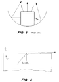
- Figure 1 shows a typical prior art LED chip in a reflector cup with light radiating from the top and the sides of the chip.
- the reflector cup collects light radiating from the sides of the LED chip and directs the light towards a useful direction.
- Figure 2 shows a light ray incident at a boundary, with an incident angle ⁇ it , between an optically transparent material with refractive index ⁇ 2 and a surrounding medium with refractive index ⁇ 1 .
- ⁇ c the critical angle
- Figures 3A-B show total internal reflections of light rays inside a rectangular shaped block of an optically transparent material which has a refractive index bigger than the refractive index of the medium surrounding the block.
- a ray emits from left hand bottom corner of the block making an angle ⁇ eb with respect to the bottom surface of the block and an angle ⁇ es with respect to the side surface of the block. Since the block is rectangular, the ray will hit the top surface of the block with an incident angle ⁇ it which is equal to ⁇ es .
- Figure 3A shows ⁇ es greater than the critical angle ⁇ c so the ray will be totally internally reflected at an angle ⁇ it and will hit the right hand side surface of the block with an incident angle ⁇ is .
- ⁇ is is equal to ⁇ eb .
- ⁇ is > ⁇ c , the ray incident onto the right hand side surface will be totally internally reflected back onto the bottom surface of the block.
- a ray emitted from the left hand top corner of the block makes an angle ⁇ ef with respect to the top surface of the block and hits the right hand side surface of the block with an incident angle of ⁇ is . Since the block is rectangular, ⁇ is is equal to ⁇ ef and if ⁇ is is greater than the critical angle, the ray will be reflected to the bottom surface of the block.
- Figure 4A shows a prior art LED using a thin electrically conductive window layer between the top metal contact and the light generation region to minimize current crowding. This feature is described in US Patent 5,008,718.
- Figure 4C shows how the normalized intensity of light emitted from the LED, I, varies as the thickness, D, of the thin window layer varies. Due to the shadowing effect of the top metal contact covering part of the thin window layer, the intensity of light is also not constant across the lateral dimension of the LED.
- Figure 4C shows the relationship of the normalized intensity of light output, I, with respect to lateral position as well. This result was reported on page 1128 in the Journal of Electronic Materials, Vol. 20, No. 12, 1991 and was based on the same prior art LED described in US Patent 5,008,718.
- the prior art LED has a lateral dimension A, of 250 ⁇ m, with a 100 ⁇ m diameter top metal contact in the middle.
- Light intensity, I drops to zero at the two edges, 0 and A, of the LED, and at the area covered by the top metal contact from 0.3A to 0.7A or from 75 to 175 ⁇ m. Due to the decrease in current crowding effect, as the thickness D goes from 0.008A to 0.06A or from 2 to 15 ⁇ m, the intensity of light emitting from the LED increases. Further increases in the thickness D will not significantly decrease the current crowding effect so the prior art LED, disclosed in US Patent 5,008,718, has a preferred thickness of 5 to 15 ⁇ m. As shown in Figure 4B, an unfortunate side effect of the prior art use of such a thin window layer is that a significant amount of light is absorbed by the substrate due to total internal reflection within the thin window layer.
- FIG. 5 shows a cross-section of an LED 100 which is constructed in accordance with a first preferred embodiment of the present invention.
- LED 100 has a top metal contact 101, a top thick transparent layer 102, a light generation region 103, a light absorbing substrate 105 and a bottom metal contact 106.
- the top thick transparent layer 102 has a lateral dimension A and a thickness D. In the following calculation of the thickness, D, the metal contact is removed and the light generation region 103 is assumed to be negligibly thin.
- Figures 6A-C show the internal light rays of the LED 100 with ⁇ c ⁇ 45°.
- the light rays emitting from the light generation region 103 radiate out of the LED 100 through its top surface 110 or its side surfaces 111.
- Figure 6B shows the benefit of a thick transparent layer 102 where light rays emit out of the side surface 111 of the transparent layer 102 instead of being absorbed by the substrate 105.
- Figure 6C shows the controlling optical path to decide the aspect ratio, D/A, of the thick transparent layer 102 in order to maximize the amount of light rays radiating from the side surfaces 111 of the LED 100.
- the minimum aspect ratio, D/A for this ray to emit out of the LED 100 without being absorbed by the substrate 105, is achieved when this ray hits the bottom right hand corner of the thick transparent layer 102.
- the thick transparent layer 102 is rectangular so the side surfaces 111 are of the same height.
- the point of incidence by the ray hitting the top surface 110 of the thick transparent layer 102 is the middle point of the lateral dimension, A, of the thick transparent layer 102.
- the thick transparent layer 102 can be very thick such as for mechanical support of the LED, but it takes a lot of time to build very thick layer.
- Figures 7A-C show the internal light rays of the LED 100 shown in Figure 5 with ⁇ c > 45°.
- Figure 7B shows the benefit of a thick transparent layer 102 where light rays emit out of the side surface 111 of the transparent layer 102 instead of being absorbed by the substrate 105.
- Figure 7C shows the controlling optical path to decide the aspect ratio, D/A, of the thick transparent layer 102 in order to maximize the amount of light rays radiating from the side surfaces 111 of the LED 100.
- ⁇ es slightly bigger than ⁇ c
- the minimum aspect ratio, D/A for this ray to emit out of the LED 100 without being absorbed by the substrate 105, is achieved when this ray hits the bottom right hand corner of the thick transparent layer 102.
- the thick transparent layer 102 is rectangular so the side surfaces 111 are of the same height.
- the point of incidence by the ray hitting the top surface 110 of the thick transparent layer 102 is the middle point of the lateral dimension, A, of the thick transparent layer 102.
- D is equal to (A/2) * (tan (90° - ⁇ c )).
- the thick transparent layer 102 can be very thick such as for mechanical support of the LED, but it takes a lot of time to build very thick layer.
- the inventors fabricated an LED 100, as shown in Figures 5-7, in which the light absorbing substrate 105 is a GaAs substrate between 150 to 200 ⁇ m thick and has a top cross-section that is 250 ⁇ m by 250 ⁇ m.
- the light generation region 103 fabricated by a metal-organic chemical vapor deposition (MOCVD) process, is a conventional double heterostructure composed of an n-type bottom confining layer of AlGaInP on top of the substrate 105, an active layer of n-type AlGaInP above the bottom confining layer and a top p-type confining layer of AlGaInP above the active layer.
- MOCVD metal-organic chemical vapor deposition
- the top and bottom confining layers have a thickness of approximately 800 nm and the active layer has a thickness of about 500 nm.
- Zinc, carbon or magnesium are suitable p-type dopants, while tellurium, selenium, sulfur and silicon are suitable n-type dopants.
- the light generation region 103 could also be fabricated as a homojunction structure instead of a heterojunction LED.
- Covering the top confining layer is the thick transparent layer 102 of GaP, fabricated by a vapor phase epitaxial process (VPE).
- VPE vapor phase epitaxial process
- the GaP thick transparent layer 102 has a resistivity of approximately 0.05 ohm-centimeter and the top confining layer has a resistivity of approximately 0.5 ohm-centimeter.
- Other materials such as AlGaAs and GaAsP that have bandgaps larger than the bandgap of the light generation region 103 can be used for the thick transparent layer 102.
- the entire LED 100 is embedded in epoxy which has a refractive index of 1.5. With GaP having a refractive index of 3.3, the critical angle, ⁇ c , is 27°. With A being 250 ⁇ m, the preferred thickness D of the thick transparent layer 102 is calculated to be 64 ⁇ m because D is defined as A*(tan ⁇ c )/2,.
- the actual LED 100 constructed by the inventors has a transparent layer 102 with a thickness, D, of 45 ⁇ m and the inventors measured light output efficiency to be 40 lumens/A.
- the estimated light output efficiency with a 64 ⁇ m transparent layer 102 is about 45 lumens/A.
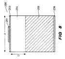
- FIG 8 shows a cross-section of an LED 200 constructed in accordance with an illustrative embodiment. Such an LED is also described in EP-A-0 350 242.
- LED 200 has a top metal contact 201, a light generation region 203, a bottom thick transparent layer 204, a light absorbing substrate 205 and a bottom metal contact 206.
- LED 200 may be constructed with the same general materials and processes as the LED 100 shown in Figure 5.
- the bottom thick transparent layer 204 has a lateral dimension A and a thickness D. In the following calculation of the thickness, D, the light generation region 203 is assumed to be negligibly thin.
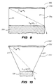
- Figure 10 shows a cross section of part of an LED constructed in accordance with a modified version of LED 200 shown in Figure 8.
- the modified version 200' shows an example of a non-parallel funnel-shaped bottom transparent layer 204'.
- the ray still hits the side surface 211' with an incidence angle ⁇ is ⁇ ⁇ c and will emit out of the LED 200'.
- More light can radiate out of the bottom transparent layer 204' if the side surfaces 211' of the thick transparent layer 204' are not parallel to each other since more rays of light will hit the side surfaces 211' with an angle less than the critical angle.
- FIG 11 shows a cross-section of an LED 300 constructed in accordance with a second preferred embodiment of the present invention.
- LED 300 has a top metal contact 301, a top thick transparent layer 302, a light generation region 303, a bottom thick transparent layer 304, a light absorbing substrate 305 and a bottom metal contact 306.
- LED 300 may be constructed with the same general materials and processes as the LED 100 shown in Figure 5.
- the top thick transparent layer 302 does not have to be made of the same material as the bottom thick transparent layer 304 and the aspect ratio D T /A should be determined as discussed above with reference to Figures 5-7.
- the aspect ratio D B /A should be determined as discussed above with reference to Figures 8-9.
- top thick transparent layer 302 is made of the same material as the bottom thick transparent layer 304 or is made of a material with a critical angle less than the critical angle of the bottom thick transparent layer 304, then the aspect ratio D T /A can be less than those discussed above with reference to Figures 5-7.
- Figure 12 shows a top thick transparent layer 302 and the bottom thick transparent layer 304 having the same critical angle, ⁇ c . Since the structure is rectangular, all the light rays with an emission angle ⁇ eb ⁇ ⁇ c will go out of the LED 300.
- the top transparent layer 302 should be thick enough to minimize the effect of current crowding but does not have to be very thick so as to extract light rays from its edges since the light rays can emit out of the side surfaces 311 of the bottom thick transparent layer 304.
- the transparent layers 302 and 304 can be very thick such as for mechanical support of the LED, but it takes a lot of time to build very thick layers.
- Figures 13A-D show a preferred method to fabricate the LED 100 shown in Figures 5-7.
- Figure 13A shows that using a MOCVD process or a molecular beam epitaxial (MBE) process in a growth chamber, the active layer 103'' and the confining layers 103' and 103''' are first epitaxially grown on top of the GaAs substrate 105. Then, as shown in Figure 13B, without removing the partially fabricated LED 100 from the growth chamber and immediately following the growth of the top confining layer 103', a thin layer 102' is grown on the top confining layer 103'. This thin layer 102' does not have to be of the same material as the final thick transparent layer 102.
- MBE molecular beam epitaxial
- this thin layer 102' is about 2 ⁇ m thick. Since the top confining layer 103' has aluminum in it, without the thin layer 102' as a protection, the top confining layer 103' can oxidize, which will detrimentally affect future epitaxial growth. Moreover, the thin layer 102' helps as a transition layer to localize dislocations due to lattice mismatch between the top confining layer 103' and the thick transparent layer 102. The localization enhances future epitaxial growth of the thick transparent layer 102.
- the thin layer 102' can be GaP or GaAsP or GaAs or AlGaAs.
- the partially fabricated LED 100 is transported for growing a top thick transparent layer 102 using a different process.
- Liquid phase epitaxial (LPE) process or vapor phase epitaxial (VPE) process is used to grow the thick transparent layer 102 to a thickness of tens of microns.
- the top thick transparent layer 102 can be GaP or GaAsP or AlGaAs. If the top thick transparent layer 102 is AlGaAs, the preferred material for the thin layer 102' should be GaAs or AlGaAs.
- the thin layer 102' should be removed before growing the thick transparent layer 102.
- LPE to grow the thick transparent layer 102
- the thin layer 102' is removed by immersing it into the melt to grow the thick transparent layer 102.
- the temperature of the melt is first raised a few degrees to dissolve the thin layer 102' back into the melt. Then the temperature of the melt will be lowered to grow the thick transparent layer 102.
- the method of using and removing a protective layer to grow a thick epitaxial layer has been disclosed in European Patent Application EP-A-0 356 037.
- VPE the thin layer 102' can be etched off with a vaporized etchant before growing the thick transparent layer 102.
- Figure 13D shows that after growing the thick transparent layer 102, the top metal contact 101 and the bottom metal contact 106 are deposited.
Landscapes
- Led Devices (AREA)
Description
- Light emitting diodes (LEDs) having a semiconductor light generation region situated on a light absorbing substrate are widely used as light sources and are beginning to replace incandescent lamps. In order to meet the demands for light output, it is important that the overall light output efficiency of the LEDs be maximized. One improvement made in the prior art, disclosed in US Patent 5,008,718, has been to increase the LED electrical efficiency by including a thin electrically conductive transparent window layer between the light generation region and the top metal contact so that current crowding is minimized. An unfortunate shortcoming of the thin window layer has been that a significant portion of the total light generated by the light generation region is still internally reflected within the window layer and is absorbed by the substrate instead of being emitted out of the LED. Thicker window layers have been investigated in the article by R.M. Fletcher et al. in Journal of Electronic Materials, vol. 20, No. 12 (1991), pages 1125-1130, or in DE-A-40 17 632.
- In accordance with the present invention, which is set out in the appended claims, an LED includes a thick transparent layer which ensures that an increased amount of light is emitted from the sides of the LED and light absorbed by the substrate is minimized. The thickness of the transparent layer is determined as a function of the width of the transparent layer and the critical angle at which light is internally reflected within the thick transparent layer.
- In an LED constructed in accordance with a first preferred embodiment of the present invention, the thick transparent layer overlays the light generation region which in turn overlays the light absorbing substrate. The inventors have fabricated an LED in accordance with this first embodiment which has a light output efficiency of 40 lumens/A instead of the approximately 20 lumens/A which is typical for a prior art LED having a thin electrically conductive transparent window layer. In an LED constructed in accordance with a second preferred embodiment of the present invention, a top thick transparent layer is positioned above the light generation region and a bottom thick transparent layer is positioned between the light generation region and the light absorbing substrate.
- The thick transparent layer should be made with material with a bandgap bigger than the light generation region so that the transparent layer will not absorb the light generated by the light generation region. The method to fabricate the thick transparent layer may be different from the method used to make the light generation region because certain methods may be more suitable to build thick epitaxial layers.
- Exemplary embodiments of the invention will now be described with reference to the following drawings:
- Figure 1 shows a typical prior art LED in a reflector cup.
- Figure 2 shows light refraction at the critical angle c.
- Figures 3A-B show total internal reflections of light rays inside a rectangular shaped transparent layer.
- Figures 4A-C show a prior art LED including a thin electrically conductive transparent window layer and the intensity of the emitted light as a function of the thickness of the window layer.
- Figure 5 shows a cross section of an LED constructed in accordance with a first preferred embodiment of the present invention.
- Figures 6A-C show internal light paths within the LED shown in Figure 5 with c ≤ 45°
- Figures 7A-C show internal light paths within the LED shown in Figure 5 with c > 45°.
- Figure 8 shows a cross section of an illustrative LED.
- Figure 9 shows an internal light path within the LED shown in Figure 8.
- Figure 10 shows a cross section of part of another illustrative LED.
- Figure 11 shows a cross section of an LED constructed in accordance with the second preferred embodiment of the present invention.
- Figure 12 shows internal light paths within the LED shown in Figure 11.
- Figures 13A-D show the process steps to fabricate the first preferred embodiment of the present invention.
-
- Figure 1 shows a typical prior art LED chip in a reflector cup with light radiating from the top and the sides of the chip. The reflector cup collects light radiating from the sides of the LED chip and directs the light towards a useful direction.
- Figure 2 shows a light ray incident at a boundary, with an incident angle it, between an optically transparent material with refractive index η2 and a surrounding medium with refractive index η1. At the boundary, there is the critical angle, c, which is defined as c = Sin-1(η1/η2). If it ≤ c, the ray will be refracted and emitted out of the optically transparent material. With the incident angle it being equal to the critical angle c, the light ray will be emitted at a direction parallel to the surface of the material as shown in Figure 2. For it > c, the ray of light will be totally internally reflected.
- Figures 3A-B show total internal reflections of light rays inside a rectangular shaped block of an optically transparent material which has a refractive index bigger than the refractive index of the medium surrounding the block. In Figure 3A, a ray emits from left hand bottom corner of the block making an angle eb with respect to the bottom surface of the block and an angle es with respect to the side surface of the block. Since the block is rectangular, the ray will hit the top surface of the block with an incident angle it which is equal to es. Figure 3A shows es greater than the critical angle c so the ray will be totally internally reflected at an angle it and will hit the right hand side surface of the block with an incident angle is. Again, since the block is rectangular and the two side surfaces are parallel, is is equal to eb. With is > c, the ray incident onto the right hand side surface will be totally internally reflected back onto the bottom surface of the block.
- In Figure 3B, a ray emitted from the left hand top corner of the block makes an angle ef with respect to the top surface of the block and hits the right hand side surface of the block with an incident angle of is. Since the block is rectangular, is is equal to ef and if is is greater than the critical angle, the ray will be reflected to the bottom surface of the block.
- Figure 4A shows a prior art LED using a thin electrically conductive window layer between the top metal contact and the light generation region to minimize current crowding. This feature is described in US Patent 5,008,718. Figure 4C shows how the normalized intensity of light emitted from the LED, I, varies as the thickness, D, of the thin window layer varies. Due to the shadowing effect of the top metal contact covering part of the thin window layer, the intensity of light is also not constant across the lateral dimension of the LED. Figure 4C shows the relationship of the normalized intensity of light output, I, with respect to lateral position as well. This result was reported on page 1128 in the Journal of Electronic Materials, Vol. 20, No. 12, 1991 and was based on the same prior art LED described in US Patent 5,008,718. The prior art LED has a lateral dimension A, of 250 µm, with a 100 µm diameter top metal contact in the middle. Light intensity, I, drops to zero at the two edges, 0 and A, of the LED, and at the area covered by the top metal contact from 0.3A to 0.7A or from 75 to 175 µm. Due to the decrease in current crowding effect, as the thickness D goes from 0.008A to 0.06A or from 2 to 15 µm, the intensity of light emitting from the LED increases. Further increases in the thickness D will not significantly decrease the current crowding effect so the prior art LED, disclosed in US Patent 5,008,718, has a preferred thickness of 5 to 15 µm. As shown in Figure 4B, an unfortunate side effect of the prior art use of such a thin window layer is that a significant amount of light is absorbed by the substrate due to total internal reflection within the thin window layer.
- Figure 5 shows a cross-section of an
LED 100 which is constructed in accordance with a first preferred embodiment of the present invention.LED 100 has atop metal contact 101, a top thicktransparent layer 102, alight generation region 103, alight absorbing substrate 105 and abottom metal contact 106. The top thicktransparent layer 102 has a lateral dimension A and a thickness D. In the following calculation of the thickness, D, the metal contact is removed and thelight generation region 103 is assumed to be negligibly thin. - Figures 6A-C show the internal light rays of the
LED 100 with c ≤ 45°. The light rays emitting from thelight generation region 103 radiate out of theLED 100 through itstop surface 110 or itsside surfaces 111. Figure 6A shows that all the rays from the left corner of thelight generation region 103 with es ≤ c radiates out of thetop surface 110 of theLED 100 because it = es which is less than or equal to c. Figure 6B shows the benefit of a thicktransparent layer 102 where light rays emit out of theside surface 111 of thetransparent layer 102 instead of being absorbed by thesubstrate 105. - Figure 6C shows the controlling optical path to decide the aspect ratio, D/A, of the thick
transparent layer 102 in order to maximize the amount of light rays radiating from theside surfaces 111 of theLED 100. All the light rays hitting theside surface 111 of theLED 100 with an incident angle, is, less than or equal to c will emit out of theLED 100. Since eb = is, this means that all the rays with eb from 0° to c will radiate out of theLED 100. The controlling ray is the ray with an emission angle eb = c. With c ≤ 45°, this controlling ray will hit thetop surface 110 of the thicktransparent layer 102 with an incident angle it > c because it = 90° - c. Since the angle of incidence is equal to the angle of reflection, the ray hitting thetop surface 110 will be totally internally reflected with an angle it. The minimum aspect ratio, D/A, for this ray to emit out of theLED 100 without being absorbed by thesubstrate 105, is achieved when this ray hits the bottom right hand corner of the thicktransparent layer 102. The thicktransparent layer 102 is rectangular so the side surfaces 111 are of the same height. With eb = is, the point of incidence by the ray hitting thetop surface 110 of the thicktransparent layer 102 is the middle point of the lateral dimension, A, of the thicktransparent layer 102. This means that D is equal to (A/2) * (tan c). If D is less than A *(tan c)/2, some of the light rays that should be able to emit out of the LED will be absorbed by thelight absorbing substrate 105. So light output efficiency increases as D increases to D = A*(tan c)/2 and then remains roughly constant. The thicktransparent layer 102 can be very thick such as for mechanical support of the LED, but it takes a lot of time to build very thick layer. Moreover light output may be decreased if D is significantly higher than D = A*(tan c)/2 because total series electrical resistance and light absorption within the thicktransparent layer 102 might significantly increase. Therefore, it might be appropriate to have the thickness, D, of the thicktransparent layer 102 not significantly more than 4 times of (A * (tan c)/2). - Figures 7A-C show the internal light rays of the
LED 100 shown in Figure 5 with c > 45°. Figure 7A shows that all the rays from the left corner of thelight generation region 103 with es ≤ c will radiate out of thetop surface 110 of theLED 100 because it = es ≤ c. Figure 7B shows the benefit of a thicktransparent layer 102 where light rays emit out of theside surface 111 of thetransparent layer 102 instead of being absorbed by thesubstrate 105. - Figure 7C shows the controlling optical path to decide the aspect ratio, D/A, of the thick
transparent layer 102 in order to maximize the amount of light rays radiating from the side surfaces 111 of theLED 100. With es slightly bigger than c, the emitted ray will be totally internally reflected by thetop surface 110 of the thicktransparent layer 102 because it = es > c. The minimum aspect ratio, D/A, for this ray to emit out of theLED 100 without being absorbed by thesubstrate 105, is achieved when this ray hits the bottom right hand corner of the thicktransparent layer 102. The thicktransparent layer 102 is rectangular so the side surfaces 111 are of the same height. With eb = is, the point of incidence by the ray hitting thetop surface 110 of the thicktransparent layer 102 is the middle point of the lateral dimension, A, of the thicktransparent layer 102. This means that D is equal to (A/2) * (tan (90° - c)). Light output efficiency increases as D increases to D = A*(tan (90° - c))/2 and then remains roughly constant. The thicktransparent layer 102 can be very thick such as for mechanical support of the LED, but it takes a lot of time to build very thick layer. Moreover light output may be decreased if D is significantly higher than D = A*(tan (90° - c))/2 because total series electrical resistance and light absorption within the thicktransparent layer 102 might significantly increase. Therefore, it might be appropriate to have the thickness, D, of the thicktransparent layer 102 not significantly more than 4 times of (A * (tan (90° - c))/2). - The inventors fabricated an
LED 100, as shown in Figures 5-7, in which thelight absorbing substrate 105 is a GaAs substrate between 150 to 200 µm thick and has a top cross-section that is 250 µm by 250 µm. Thelight generation region 103, fabricated by a metal-organic chemical vapor deposition (MOCVD) process, is a conventional double heterostructure composed of an n-type bottom confining layer of AlGaInP on top of thesubstrate 105, an active layer of n-type AlGaInP above the bottom confining layer and a top p-type confining layer of AlGaInP above the active layer. The top and bottom confining layers have a thickness of approximately 800 nm and the active layer has a thickness of about 500 nm. Zinc, carbon or magnesium are suitable p-type dopants, while tellurium, selenium, sulfur and silicon are suitable n-type dopants. Thelight generation region 103 could also be fabricated as a homojunction structure instead of a heterojunction LED. Covering the top confining layer is the thicktransparent layer 102 of GaP, fabricated by a vapor phase epitaxial process (VPE). The thicktransparent layer 102, with a lateral dimension of 250 µm, should be at least 15 µm thick to minimize the effect of current crowding. The GaP thicktransparent layer 102 has a resistivity of approximately 0.05 ohm-centimeter and the top confining layer has a resistivity of approximately 0.5 ohm-centimeter. Other materials such as AlGaAs and GaAsP that have bandgaps larger than the bandgap of thelight generation region 103 can be used for the thicktransparent layer 102. Theentire LED 100 is embedded in epoxy which has a refractive index of 1.5. With GaP having a refractive index of 3.3, the critical angle, c, is 27°. With A being 250 µm, the preferred thickness D of the thicktransparent layer 102 is calculated to be 64 µm because D is defined as A*(tan c)/2,. Theactual LED 100 constructed by the inventors has atransparent layer 102 with a thickness, D, of 45 µm and the inventors measured light output efficiency to be 40 lumens/A. The estimated light output efficiency with a 64 µmtransparent layer 102 is about 45 lumens/A. - Figure 8 shows a cross-section of an
LED 200 constructed in accordance with an illustrative embodiment. Such an LED is also described in EP-A-0 350 242.LED 200 has atop metal contact 201, alight generation region 203, a bottom thicktransparent layer 204, alight absorbing substrate 205 and abottom metal contact 206.LED 200 may be constructed with the same general materials and processes as theLED 100 shown in Figure 5. The bottom thicktransparent layer 204 has a lateral dimension A and a thickness D. In the following calculation of the thickness, D, thelight generation region 203 is assumed to be negligibly thin. - Figure 9 shows the controlling optical path to decide the aspect ratio D/A of the thick
transparent layer 204 ofLED 200. All the rays hitting theside surface 211 with an incident angle, is, less than or equal to c will radiate out of theLED 200. With is = ef, the optimal aspect ratio, D/A, of the thicktransparent layer 204 is tan c. The thicktransparent layer 204 can be very thick such as for mechanical support of the LED, but it takes a lot of time to build very thick layer. Moreover light output may be decreased if D is significantly higher than D = A * tan c because total series electrical resistance and light absorption within the thicktransparent layer 102 might significantly increase. Therefore, it might be appropriate for the thickness, D, of the thicktransparent layer 102 not significantly more than 4 times of(A * tan c). - Figure 10 shows a cross section of part of an LED constructed in accordance with a modified version of
LED 200 shown in Figure 8. The modified version 200' shows an example of a non-parallel funnel-shaped bottom transparent layer 204'. As shown in Figure 10, even if the emission angle ef > c, the ray still hits the side surface 211' with an incidence angle is < c and will emit out of the LED 200'. More light can radiate out of the bottom transparent layer 204' if the side surfaces 211' of the thick transparent layer 204' are not parallel to each other since more rays of light will hit the side surfaces 211' with an angle less than the critical angle. - Figure 11 shows a cross-section of an
LED 300 constructed in accordance with a second preferred embodiment of the present invention.LED 300 has atop metal contact 301, a top thicktransparent layer 302, alight generation region 303, a bottom thicktransparent layer 304, alight absorbing substrate 305 and abottom metal contact 306.LED 300 may be constructed with the same general materials and processes as theLED 100 shown in Figure 5. In general, the top thicktransparent layer 302 does not have to be made of the same material as the bottom thicktransparent layer 304 and the aspect ratio DT/A should be determined as discussed above with reference to Figures 5-7. The aspect ratio DB/A should be determined as discussed above with reference to Figures 8-9. - However, if the top thick
transparent layer 302 is made of the same material as the bottom thicktransparent layer 304 or is made of a material with a critical angle less than the critical angle of the bottom thicktransparent layer 304, then the aspect ratio DT/A can be less than those discussed above with reference to Figures 5-7. Figure 12 shows a top thicktransparent layer 302 and the bottom thicktransparent layer 304 having the same critical angle, c. Since the structure is rectangular, all the light rays with an emission angle eb ≤ c will go out of theLED 300. This is because if the light ray is totally internally reflected by thetop surface 310, it will hit theside surface 311 with an incident angle is = eb ≤ c before reaching thelight absorbing substrate 305 and will emit out of theLED 300. Thus, the toptransparent layer 302 should be thick enough to minimize the effect of current crowding but does not have to be very thick so as to extract light rays from its edges since the light rays can emit out of the side surfaces 311 of the bottom thicktransparent layer 304. However, thetransparent layers transparent layers transparent layer 304 not significantly more than 4 times of A * tan c. - Figures 13A-D show a preferred method to fabricate the
LED 100 shown in Figures 5-7. Figure 13A shows that using a MOCVD process or a molecular beam epitaxial (MBE) process in a growth chamber, the active layer 103'' and the confining layers 103' and 103''' are first epitaxially grown on top of theGaAs substrate 105. Then, as shown in Figure 13B, without removing the partially fabricatedLED 100 from the growth chamber and immediately following the growth of the top confining layer 103', a thin layer 102' is grown on the top confining layer 103'. This thin layer 102' does not have to be of the same material as the final thicktransparent layer 102. Serving as a protective and a transition layer, this thin layer 102' is about 2 µm thick. Since the top confining layer 103' has aluminum in it, without the thin layer 102' as a protection, the top confining layer 103' can oxidize, which will detrimentally affect future epitaxial growth. Moreover, the thin layer 102' helps as a transition layer to localize dislocations due to lattice mismatch between the top confining layer 103' and the thicktransparent layer 102. The localization enhances future epitaxial growth of the thicktransparent layer 102. The thin layer 102' can be GaP or GaAsP or GaAs or AlGaAs. - It is both expensive and difficult to grow thick layers with a MOCVD process or a MBE process. As shown in Figure 13C, with the thin layer 102' in place, the partially fabricated
LED 100 is transported for growing a top thicktransparent layer 102 using a different process. Liquid phase epitaxial (LPE) process or vapor phase epitaxial (VPE) process is used to grow the thicktransparent layer 102 to a thickness of tens of microns. The top thicktransparent layer 102 can be GaP or GaAsP or AlGaAs. If the top thicktransparent layer 102 is AlGaAs, the preferred material for the thin layer 102' should be GaAs or AlGaAs. - If the thin layer 102' is made of GaAs or AlGaAs, then the thin layer 102' should be removed before growing the thick
transparent layer 102. With LPE to grow the thicktransparent layer 102, the thin layer 102' is removed by immersing it into the melt to grow the thicktransparent layer 102. The temperature of the melt is first raised a few degrees to dissolve the thin layer 102' back into the melt. Then the temperature of the melt will be lowered to grow the thicktransparent layer 102. The method of using and removing a protective layer to grow a thick epitaxial layer has been disclosed in European Patent Application EP-A-0 356 037. With VPE, the thin layer 102' can be etched off with a vaporized etchant before growing the thicktransparent layer 102. Figure 13D shows that after growing the thicktransparent layer 102, thetop metal contact 101 and thebottom metal contact 106 are deposited.
Claims (7)
- A light emitting diode (100), positioned in a medium having a refractive index, n1, the light emitting diode having a width, A, and comprising:a light absorbing substrate (105);a light generation region (103) overlaying the substrate (105);a first transparent layer (102) overlaying the light generation region, the first transparent layer having sides with a thickness, D, which is greater than a minimum thickness of about 0.06 times A, and a refractive index n2; where n1 and n2 define a critical angle Θc = Sin-1 (n1/n2); and (a) the thickness D of the first transparent layer (102) is between one times and less than 4 times (A * tan Θc)/2 if the critical angle Θc ≤ 45°, or (b) the thickness D of the first transparent layer (102) is between one times and less than 4 times A * tan (90° -Θc)/2, if critical angle Θc > 45°,wherein the first transparent layer (102) increases the light generation efficiency of the light emitting diode by increasing an amount of light emitted from the sides and reducing an amount of light absorbed by the light absorbing substrate (105).
- A light emitting diode (100,200,200') as recited in claim 1, wherein the first transparent layer (102,204,204') is selected from the group comprising GaP, GaAsP and A1GaAs.
- A light emitting diode (300) as recited in claim 1, further comprising a second transparent layer (304) between the light generation region (303) and the light absorbing substrate (305).
- A light emitting diode (300) as recited in claim 3, wherein the second transparent layer (304) has a refractive index, n1 and n2 defines a critical angle Θc = Sin-1 (n1/n2); andthe thickness, D, of the second transparent layer (304) is less than 4 times A * tan Θc.
- A light emitting diode (300) as recited in claim 4, wherein:the first transparent layer (302) as selected from the group comprising GaP, GaAsP and A1GaAs; andthe second transparent layer (304) is selected from the group comprising GaP, GaAsP and A1GaAs.
- A process of producing a light emitting diode (100,200,200') as recited in claim 1 or 2, comprising the steps of fabricating the light generation region (103,203,203') by a first process chosen from the group of metal-organic vapour deposition and molecular beam epitaxy; and fabricating the first transparent layer (102,204,204') by a second process chosen from the group of vapour phase epitaxy and liquid phase epitaxy.
- A process of producing a light emitting diode (300) as recited in claim 3,4 or 5, comprising the steps of fabricating the light generation region (303) by a first process; fabricating the first transparent layer (302) by a second process; and fabricating the second transparent layer (304) by a third process, wherein the first process is chosen from the group of metal-organic vapour deposition and molecular beam epitaxy, and the second and third processes are chosen from the group of vapour phase epitaxy and liquid phase epitaxy.
Applications Claiming Priority (2)
| Application Number | Priority Date | Filing Date | Title |
|---|---|---|---|
| US07/819,542 US5233204A (en) | 1992-01-10 | 1992-01-10 | Light-emitting diode with a thick transparent layer |
| US819542 | 1992-01-10 |
Publications (2)
| Publication Number | Publication Date |
|---|---|
| EP0551001A1 EP0551001A1 (en) | 1993-07-14 |
| EP0551001B1 true EP0551001B1 (en) | 1999-09-15 |
Family
ID=25228430
Family Applications (1)
| Application Number | Title | Priority Date | Filing Date |
|---|---|---|---|
| EP92311706A Expired - Lifetime EP0551001B1 (en) | 1992-01-10 | 1992-12-22 | Light-emitting diode with a thick transparent layer |
Country Status (4)
| Country | Link |
|---|---|
| US (1) | US5233204A (en) |
| EP (1) | EP0551001B1 (en) |
| JP (1) | JP3639608B2 (en) |
| DE (1) | DE69229991T2 (en) |
Cited By (1)
| Publication number | Priority date | Publication date | Assignee | Title |
|---|---|---|---|---|
| US7268371B2 (en) | 1997-06-03 | 2007-09-11 | Philips Lumileds Lighting Company, Llc | Light extraction from a semiconductor light emitting device via chip shaping |
Families Citing this family (92)
| Publication number | Priority date | Publication date | Assignee | Title |
|---|---|---|---|---|
| US6590502B1 (en) | 1992-10-12 | 2003-07-08 | 911Ep, Inc. | Led warning signal light and movable support |
| US5481122A (en) * | 1994-07-25 | 1996-01-02 | Industrial Technology Research Institute | Surface light emitting diode with electrically conductive window layer |
| US5811839A (en) * | 1994-09-01 | 1998-09-22 | Mitsubishi Chemical Corporation | Semiconductor light-emitting devices |
| US6996150B1 (en) | 1994-09-14 | 2006-02-07 | Rohm Co., Ltd. | Semiconductor light emitting device and manufacturing method therefor |
| JP3442889B2 (en) | 1994-12-27 | 2003-09-02 | 株式会社東芝 | Semiconductor light emitting device |
| US5671996A (en) * | 1994-12-30 | 1997-09-30 | Donnelly Corporation | Vehicle instrumentation/console lighting |
| DE19629920B4 (en) * | 1995-08-10 | 2006-02-02 | LumiLeds Lighting, U.S., LLC, San Jose | Light-emitting diode with a non-absorbing distributed Bragg reflector |
| DE19537543A1 (en) * | 1995-10-09 | 1997-04-10 | Telefunken Microelectron | Light emitting diode |
| JP3233569B2 (en) * | 1996-03-22 | 2001-11-26 | シャープ株式会社 | Semiconductor light emitting device |
| JPH09283798A (en) | 1996-04-19 | 1997-10-31 | Rohm Co Ltd | Semiconductor light emitting device and method of manufacturing the same |
| US5705834A (en) * | 1996-04-23 | 1998-01-06 | The United States Of America As Represented By The Administrator Of The National Aeronautics And Space Administration | Increased efficiency LED |
| DE59705207D1 (en) | 1996-08-07 | 2001-12-06 | Osram Opto Semiconductors Gmbh | METHOD FOR PRODUCING AN INFRARED-EMITTING LUMINESCENCE DIODE |
| DE19632626A1 (en) * | 1996-08-13 | 1998-02-19 | Siemens Ag | Method for manufacturing semiconductor bodies with MOVPE layer sequence |
| US6031958A (en) * | 1997-05-21 | 2000-02-29 | Mcgaffigan; Thomas H. | Optical light pipes with laser light appearance |
| US6229160B1 (en) * | 1997-06-03 | 2001-05-08 | Lumileds Lighting, U.S., Llc | Light extraction from a semiconductor light-emitting device via chip shaping |
| AU747260B2 (en) | 1997-07-25 | 2002-05-09 | Nichia Chemical Industries, Ltd. | Nitride semiconductor device |
| DE19741609C2 (en) | 1997-09-20 | 2003-02-27 | Vishay Semiconductor Gmbh | Use of a superlattice structure comprising a plurality of heterojunction layer layers arranged one behind the other to improve the lateral current propagation in a light-emitting semiconductor diode |
| GB2330679B (en) | 1997-10-21 | 2002-04-24 | 911 Emergency Products Inc | Warning signal light |
| US6100544A (en) * | 1998-05-20 | 2000-08-08 | Visual Photonics Epitaxy Co., Ltd. | Light-emitting diode having a layer of AlGaInP graded composition |
| US20010020703A1 (en) | 1998-07-24 | 2001-09-13 | Nathan F. Gardner | Algainp light emitting devices with thin active layers |
| US6207972B1 (en) | 1999-01-12 | 2001-03-27 | Super Epitaxial Products, Inc. | Light emitting diode with transparent window layer |
| JP3472714B2 (en) | 1999-01-25 | 2003-12-02 | シャープ株式会社 | Method for manufacturing semiconductor light emitting device |
| JP3770014B2 (en) | 1999-02-09 | 2006-04-26 | 日亜化学工業株式会社 | Nitride semiconductor device |
| ATE452445T1 (en) | 1999-03-04 | 2010-01-15 | Nichia Corp | NITRIDE SEMICONDUCTOR LASER ELEMENT |
| US6614359B2 (en) | 1999-04-06 | 2003-09-02 | 911 Emergency Products, Inc. | Replacement led lamp assembly and modulated power intensity for light source |
| US6462669B1 (en) | 1999-04-06 | 2002-10-08 | E. P . Survivors Llc | Replaceable LED modules |
| US6380865B1 (en) | 1999-04-06 | 2002-04-30 | 911 Emergency Products, Inc. | Replacement led lamp assembly and modulated power intensity for light source |
| US6258699B1 (en) | 1999-05-10 | 2001-07-10 | Visual Photonics Epitaxy Co., Ltd. | Light emitting diode with a permanent subtrate of transparent glass or quartz and the method for manufacturing the same |
| TW437104B (en) | 1999-05-25 | 2001-05-28 | Wang Tien Yang | Semiconductor light-emitting device and method for manufacturing the same |
| US6705745B1 (en) | 1999-06-08 | 2004-03-16 | 911Ep, Inc. | Rotational led reflector |
| WO2000074975A1 (en) | 1999-06-08 | 2000-12-14 | 911 Emergency Products, Inc. | Strip led light assembly for motor vehicle |
| US6287947B1 (en) * | 1999-06-08 | 2001-09-11 | Lumileds Lighting, U.S. Llc | Method of forming transparent contacts to a p-type GaN layer |
| US6700502B1 (en) | 1999-06-08 | 2004-03-02 | 911Ep, Inc. | Strip LED light assembly for motor vehicle |
| US6133589A (en) | 1999-06-08 | 2000-10-17 | Lumileds Lighting, U.S., Llc | AlGaInN-based LED having thick epitaxial layer for improved light extraction |
| US6547410B1 (en) | 2000-07-28 | 2003-04-15 | 911 Emergency Products, Inc. | LED alley/take-down light |
| US6367949B1 (en) | 1999-08-04 | 2002-04-09 | 911 Emergency Products, Inc. | Par 36 LED utility lamp |
| US6623151B2 (en) | 1999-08-04 | 2003-09-23 | 911Ep, Inc. | LED double light bar and warning light signal |
| DE19943406C2 (en) | 1999-09-10 | 2001-07-19 | Osram Opto Semiconductors Gmbh | Light emitting diode with surface structuring |
| US6577658B1 (en) | 1999-09-20 | 2003-06-10 | E20 Corporation, Inc. | Method and apparatus for planar index guided vertical cavity surface emitting lasers |
| DE19947030A1 (en) | 1999-09-30 | 2001-04-19 | Osram Opto Semiconductors Gmbh | Surface-structured light emission diode with improved current coupling |
| US6287882B1 (en) | 1999-10-04 | 2001-09-11 | Visual Photonics Epitaxy Co., Ltd. | Light emitting diode with a metal-coated reflective permanent substrate and the method for manufacturing the same |
| JP2001267631A (en) | 2000-01-11 | 2001-09-28 | Sharp Corp | Semiconductor light emitting device |
| DE10006738C2 (en) | 2000-02-15 | 2002-01-17 | Osram Opto Semiconductors Gmbh | Light-emitting component with improved light decoupling and method for its production |
| WO2001061765A1 (en) * | 2000-02-15 | 2001-08-23 | Osram Opto Semiconductors Gmbh | Semiconductor component which emits radiation, and method for producing the same |
| DE10019665A1 (en) * | 2000-04-19 | 2001-10-31 | Osram Opto Semiconductors Gmbh | Luminescent diode chip and method for its production |
| DE20111659U1 (en) * | 2000-05-23 | 2001-12-13 | OSRAM Opto Semiconductors GmbH & Co. oHG, 93049 Regensburg | Component for optoelectronics |
| US6590343B2 (en) | 2000-06-06 | 2003-07-08 | 911Ep, Inc. | LED compensation circuit |
| DE10056292A1 (en) | 2000-11-14 | 2002-09-19 | Osram Opto Semiconductors Gmbh | emitting diode |
| WO2002041276A2 (en) * | 2000-11-15 | 2002-05-23 | Snowy Village, Inc. | Led warning light and communication system |
| US8188878B2 (en) | 2000-11-15 | 2012-05-29 | Federal Law Enforcement Development Services, Inc. | LED light communication system |
| US7439847B2 (en) | 2002-08-23 | 2008-10-21 | John C. Pederson | Intelligent observation and identification database system |
| US6940704B2 (en) | 2001-01-24 | 2005-09-06 | Gelcore, Llc | Semiconductor light emitting device |
| DE10120703A1 (en) | 2001-04-27 | 2002-10-31 | Osram Opto Semiconductors Gmbh | Semiconductor chip for optoelectronics |
| DE10148227B4 (en) * | 2001-09-28 | 2015-03-05 | Osram Opto Semiconductors Gmbh | Radiation-emitting semiconductor chip, method for its production and radiation-emitting component |
| CN100392873C (en) * | 2001-12-07 | 2008-06-04 | 张修恒 | Structure and method for packaging colour light-emitting diode with stacked wafer |
| JP3776824B2 (en) | 2002-04-05 | 2006-05-17 | 株式会社東芝 | Semiconductor light emitting device and manufacturing method thereof |
| US6777257B2 (en) * | 2002-05-17 | 2004-08-17 | Shin-Etsu Handotai Co., Ltd. | Method of fabricating a light emitting device and light emitting device |
| US6890781B2 (en) * | 2002-06-25 | 2005-05-10 | Uni Light Technology Inc. | Transparent layer of a LED device and the method for growing the same |
| JP2004128452A (en) * | 2002-07-31 | 2004-04-22 | Shin Etsu Handotai Co Ltd | Light emitting device manufacturing method and light emitting device |
| WO2004015784A2 (en) * | 2002-07-31 | 2004-02-19 | Firecomms Limited | A light emitting diode |
| DE10239045A1 (en) * | 2002-08-26 | 2004-03-11 | Osram Opto Semiconductors Gmbh | Method for producing an electromagnetic radiation-emitting semiconductor chip and electromagnetic radiation-emitting semiconductor chip |
| JP4080843B2 (en) | 2002-10-30 | 2008-04-23 | 株式会社東芝 | Nonvolatile semiconductor memory device |
| US20040227141A1 (en) * | 2003-01-30 | 2004-11-18 | Epistar Corporation | Light emitting device having a high resistivity cushion layer |
| JP5032130B2 (en) * | 2004-01-26 | 2012-09-26 | オスラム オプト セミコンダクターズ ゲゼルシャフト ミット ベシュレンクテル ハフツング | Thin film LED having current diffusion structure |
| DE102004025610A1 (en) | 2004-04-30 | 2005-11-17 | Osram Opto Semiconductors Gmbh | Optoelectronic component with several current spreading layers and method for its production |
| JP4371029B2 (en) | 2004-09-29 | 2009-11-25 | サンケン電気株式会社 | Semiconductor light emitting device and manufacturing method thereof |
| US7952112B2 (en) * | 2005-04-29 | 2011-05-31 | Philips Lumileds Lighting Company Llc | RGB thermal isolation substrate |
| DE102005025416A1 (en) * | 2005-06-02 | 2006-12-14 | Osram Opto Semiconductors Gmbh | Luminescence diode chip with a contact structure |
| US7772604B2 (en) | 2006-01-05 | 2010-08-10 | Illumitex | Separate optical device for directing light from an LED |
| US20070181905A1 (en) * | 2006-02-07 | 2007-08-09 | Hui-Heng Wang | Light emitting diode having enhanced side emitting capability |
| US8350279B2 (en) | 2006-09-25 | 2013-01-08 | Seoul Opto Device Co., Ltd. | Light emitting diode having AlInGaP active layer and method of fabricating the same |
| WO2008042351A2 (en) | 2006-10-02 | 2008-04-10 | Illumitex, Inc. | Led system and method |
| US9100124B2 (en) | 2007-05-24 | 2015-08-04 | Federal Law Enforcement Development Services, Inc. | LED Light Fixture |
| US9455783B2 (en) | 2013-05-06 | 2016-09-27 | Federal Law Enforcement Development Services, Inc. | Network security and variable pulse wave form with continuous communication |
| US9258864B2 (en) | 2007-05-24 | 2016-02-09 | Federal Law Enforcement Development Services, Inc. | LED light control and management system |
| US8188879B2 (en) | 2007-05-24 | 2012-05-29 | Federal Law Enforcement Development Services, Inc. | LED light global positioning and routing communication system |
| US9414458B2 (en) | 2007-05-24 | 2016-08-09 | Federal Law Enforcement Development Services, Inc. | LED light control assembly and system |
| US9294198B2 (en) | 2007-05-24 | 2016-03-22 | Federal Law Enforcement Development Services, Inc. | Pulsed light communication key |
| US11265082B2 (en) | 2007-05-24 | 2022-03-01 | Federal Law Enforcement Development Services, Inc. | LED light control assembly and system |
| US8692286B2 (en) | 2007-12-14 | 2014-04-08 | Philips Lumileds Lighing Company LLC | Light emitting device with bonded interface |
| JP2011512037A (en) | 2008-02-08 | 2011-04-14 | イルミテックス, インコーポレイテッド | System and method for emitter layer shaping |
| TWI362769B (en) | 2008-05-09 | 2012-04-21 | Univ Nat Chiao Tung | Light emitting device and fabrication method therefor |
| TW201034256A (en) | 2008-12-11 | 2010-09-16 | Illumitex Inc | Systems and methods for packaging light-emitting diode devices |
| US8890773B1 (en) | 2009-04-01 | 2014-11-18 | Federal Law Enforcement Development Services, Inc. | Visible light transceiver glasses |
| US8585253B2 (en) | 2009-08-20 | 2013-11-19 | Illumitex, Inc. | System and method for color mixing lens array |
| US8449128B2 (en) | 2009-08-20 | 2013-05-28 | Illumitex, Inc. | System and method for a lens and phosphor layer |
| CA2824756C (en) | 2011-01-14 | 2014-12-23 | Federal Law Enforcement Development Services, Inc. | Method of providing lumens and tracking of lumen consumption |
| US9265112B2 (en) | 2013-03-13 | 2016-02-16 | Federal Law Enforcement Development Services, Inc. | LED light control and management system |
| US20150198941A1 (en) | 2014-01-15 | 2015-07-16 | John C. Pederson | Cyber Life Electronic Networking and Commerce Operating Exchange |
| DE102014114613B4 (en) | 2014-10-08 | 2023-10-12 | OSRAM Opto Semiconductors Gesellschaft mit beschränkter Haftung | Radiation-emitting semiconductor chip, method for producing a large number of radiation-emitting semiconductor chips and optoelectronic component with a radiation-emitting semiconductor chip |
| US20170048953A1 (en) | 2015-08-11 | 2017-02-16 | Federal Law Enforcement Development Services, Inc. | Programmable switch and system |
| US11798974B2 (en) * | 2019-09-27 | 2023-10-24 | Seoul Viosys Co., Ltd. | Light emitting device for display and display apparatus having the same |
Family Cites Families (5)
| Publication number | Priority date | Publication date | Assignee | Title |
|---|---|---|---|---|
| JPH0728047B2 (en) * | 1986-02-17 | 1995-03-29 | 日本電気株式会社 | Phototransistor |
| US4864369A (en) * | 1988-07-05 | 1989-09-05 | Hewlett-Packard Company | P-side up double heterojunction AlGaAs light-emitting diode |
| US5153889A (en) * | 1989-05-31 | 1992-10-06 | Kabushiki Kaisha Toshiba | Semiconductor light emitting device |
| US5048035A (en) * | 1989-05-31 | 1991-09-10 | Kabushiki Kaisha Toshiba | Semiconductor light emitting device |
| US5008718A (en) * | 1989-12-18 | 1991-04-16 | Fletcher Robert M | Light-emitting diode with an electrically conductive window |
-
1992
- 1992-01-10 US US07/819,542 patent/US5233204A/en not_active Expired - Lifetime
- 1992-12-22 DE DE69229991T patent/DE69229991T2/en not_active Expired - Lifetime
- 1992-12-22 EP EP92311706A patent/EP0551001B1/en not_active Expired - Lifetime
-
1993
- 1993-01-08 JP JP01800593A patent/JP3639608B2/en not_active Expired - Lifetime
Cited By (1)
| Publication number | Priority date | Publication date | Assignee | Title |
|---|---|---|---|---|
| US7268371B2 (en) | 1997-06-03 | 2007-09-11 | Philips Lumileds Lighting Company, Llc | Light extraction from a semiconductor light emitting device via chip shaping |
Also Published As
| Publication number | Publication date |
|---|---|
| DE69229991T2 (en) | 2000-01-05 |
| JP3639608B2 (en) | 2005-04-20 |
| US5233204A (en) | 1993-08-03 |
| DE69229991D1 (en) | 1999-10-21 |
| JPH05275740A (en) | 1993-10-22 |
| EP0551001A1 (en) | 1993-07-14 |
Similar Documents
| Publication | Publication Date | Title |
|---|---|---|
| US5233204A (en) | Light-emitting diode with a thick transparent layer | |
| EP0434233B1 (en) | Light-emitting diode with an electrically conductive window layer | |
| KR100745229B1 (en) | Improved light extraction from a semiconductor light-emitting device via chip shaping | |
| EP0047591B1 (en) | Light emitting diodes with high external quantum efficiency | |
| TWI381548B (en) | Photoelectric semiconductor body and method of manufacturing the same | |
| US7993943B2 (en) | GaN based LED with improved light extraction efficiency and method for making the same | |
| US20020137244A1 (en) | Method for forming a semiconductor device having a metal substrate | |
| US20040094772A1 (en) | Gallium nitride based compound semiconductor light-emitting device and manufacturing method therefor | |
| US5103269A (en) | Electroluminescent device of compound semiconductor comprising zns or zns and znse | |
| US6107647A (en) | Semiconductor AlGaInP light emitting device | |
| US20110127554A1 (en) | Light emitting device and method of manufacturing the same | |
| US8232568B2 (en) | High brightness LED utilizing a roughened active layer and conformal cladding | |
| JP6924836B2 (en) | Optoelectronic semiconductor chip | |
| EP0616377B1 (en) | Semiconductor light-emitting element and method for its manufacturing | |
| CA1137606A (en) | Electroluminescent semiconductor device | |
| JP2004128452A (en) | Light emitting device manufacturing method and light emitting device | |
| JP2004146539A (en) | Light emitting device manufacturing method and light emitting device | |
| WO1999031738A2 (en) | Aiii-nitride channeled led | |
| JP2004186268A (en) | Light emitting element | |
| JP2004146541A (en) | Light emitting element and method of manufacturing same | |
| US6064076A (en) | Light-emitting diode having a transparent substrate | |
| US6440765B1 (en) | Method for fabricating an infrared-emitting light-emitting diode | |
| KR20190140835A (en) | Ⅲ-ⅴcompound based light emitting diode | |
| JP2004095827A (en) | Light emitting diode | |
| JP4061497B2 (en) | Method for manufacturing light emitting device |
Legal Events
| Date | Code | Title | Description |
|---|---|---|---|
| PUAI | Public reference made under article 153(3) epc to a published international application that has entered the european phase |
Free format text: ORIGINAL CODE: 0009012 |
|
| AK | Designated contracting states |
Kind code of ref document: A1 Designated state(s): DE FR GB IT |
|
| 17P | Request for examination filed |
Effective date: 19931113 |
|
| 17Q | First examination report despatched |
Effective date: 19950207 |
|
| GRAG | Despatch of communication of intention to grant |
Free format text: ORIGINAL CODE: EPIDOS AGRA |
|
| GRAG | Despatch of communication of intention to grant |
Free format text: ORIGINAL CODE: EPIDOS AGRA |
|
| GRAH | Despatch of communication of intention to grant a patent |
Free format text: ORIGINAL CODE: EPIDOS IGRA |
|
| GRAH | Despatch of communication of intention to grant a patent |
Free format text: ORIGINAL CODE: EPIDOS IGRA |
|
| GRAA | (expected) grant |
Free format text: ORIGINAL CODE: 0009210 |
|
| AK | Designated contracting states |
Kind code of ref document: B1 Designated state(s): DE FR GB IT |
|
| REF | Corresponds to: |
Ref document number: 69229991 Country of ref document: DE Date of ref document: 19991021 |
|
| ET | Fr: translation filed | ||
| ITF | It: translation for a ep patent filed | ||
| PLBE | No opposition filed within time limit |
Free format text: ORIGINAL CODE: 0009261 |
|
| STAA | Information on the status of an ep patent application or granted ep patent |
Free format text: STATUS: NO OPPOSITION FILED WITHIN TIME LIMIT |
|
| 26N | No opposition filed | ||
| REG | Reference to a national code |
Ref country code: GB Ref legal event code: 732E |
|
| PGFP | Annual fee paid to national office [announced via postgrant information from national office to epo] |
Ref country code: FR Payment date: 20010219 Year of fee payment: 9 |
|
| REG | Reference to a national code |
Ref country code: FR Ref legal event code: TP |
|
| REG | Reference to a national code |
Ref country code: FR Ref legal event code: TP |
|
| REG | Reference to a national code |
Ref country code: GB Ref legal event code: IF02 |
|
| PG25 | Lapsed in a contracting state [announced via postgrant information from national office to epo] |
Ref country code: FR Free format text: LAPSE BECAUSE OF NON-PAYMENT OF DUE FEES Effective date: 20020830 |
|
| REG | Reference to a national code |
Ref country code: FR Ref legal event code: ST |
|
| PG25 | Lapsed in a contracting state [announced via postgrant information from national office to epo] |
Ref country code: IT Free format text: LAPSE BECAUSE OF NON-PAYMENT OF DUE FEES;WARNING: LAPSES OF ITALIAN PATENTS WITH EFFECTIVE DATE BEFORE 2007 MAY HAVE OCCURRED AT ANY TIME BEFORE 2007. THE CORRECT EFFECTIVE DATE MAY BE DIFFERENT FROM THE ONE RECORDED. Effective date: 20051222 |
|
| REG | Reference to a national code |
Ref country code: GB Ref legal event code: 732E |
|
| PGFP | Annual fee paid to national office [announced via postgrant information from national office to epo] |
Ref country code: DE Payment date: 20120229 Year of fee payment: 20 |
|
| PGFP | Annual fee paid to national office [announced via postgrant information from national office to epo] |
Ref country code: GB Payment date: 20120103 Year of fee payment: 20 |
|
| REG | Reference to a national code |
Ref country code: DE Ref legal event code: R071 Ref document number: 69229991 Country of ref document: DE |
|
| REG | Reference to a national code |
Ref country code: GB Ref legal event code: PE20 Expiry date: 20121221 |
|
| PG25 | Lapsed in a contracting state [announced via postgrant information from national office to epo] |
Ref country code: GB Free format text: LAPSE BECAUSE OF EXPIRATION OF PROTECTION Effective date: 20121221 |