EP0549152A2 - Single chip controller for optical data disk drives - Google Patents
Single chip controller for optical data disk drives Download PDFInfo
- Publication number
- EP0549152A2 EP0549152A2 EP92310962A EP92310962A EP0549152A2 EP 0549152 A2 EP0549152 A2 EP 0549152A2 EP 92310962 A EP92310962 A EP 92310962A EP 92310962 A EP92310962 A EP 92310962A EP 0549152 A2 EP0549152 A2 EP 0549152A2
- Authority
- EP
- European Patent Office
- Prior art keywords
- data
- ode
- disk
- odc
- controller
- Prior art date
- Legal status (The legal status is an assumption and is not a legal conclusion. Google has not performed a legal analysis and makes no representation as to the accuracy of the status listed.)
- Ceased
Links
Images


Classifications
-
- G—PHYSICS
- G06—COMPUTING; CALCULATING OR COUNTING
- G06F—ELECTRIC DIGITAL DATA PROCESSING
- G06F3/00—Input arrangements for transferring data to be processed into a form capable of being handled by the computer; Output arrangements for transferring data from processing unit to output unit, e.g. interface arrangements
- G06F3/06—Digital input from, or digital output to, record carriers, e.g. RAID, emulated record carriers or networked record carriers
- G06F3/0601—Interfaces specially adapted for storage systems
-
- G—PHYSICS
- G11—INFORMATION STORAGE
- G11B—INFORMATION STORAGE BASED ON RELATIVE MOVEMENT BETWEEN RECORD CARRIER AND TRANSDUCER
- G11B11/00—Recording on or reproducing from the same record carrier wherein for these two operations the methods are covered by different main groups of groups G11B3/00 - G11B7/00 or by different subgroups of group G11B9/00; Record carriers therefor
-
- G—PHYSICS
- G11—INFORMATION STORAGE
- G11B—INFORMATION STORAGE BASED ON RELATIVE MOVEMENT BETWEEN RECORD CARRIER AND TRANSDUCER
- G11B20/00—Signal processing not specific to the method of recording or reproducing; Circuits therefor
- G11B20/10—Digital recording or reproducing
-
- G—PHYSICS
- G11—INFORMATION STORAGE
- G11B—INFORMATION STORAGE BASED ON RELATIVE MOVEMENT BETWEEN RECORD CARRIER AND TRANSDUCER
- G11B20/00—Signal processing not specific to the method of recording or reproducing; Circuits therefor
- G11B20/10—Digital recording or reproducing
- G11B20/12—Formatting, e.g. arrangement of data block or words on the record carriers
- G11B20/1217—Formatting, e.g. arrangement of data block or words on the record carriers on discs
- G11B20/1252—Formatting, e.g. arrangement of data block or words on the record carriers on discs for discontinuous data, e.g. digital information signals, computer programme data
-
- G—PHYSICS
- G11—INFORMATION STORAGE
- G11B—INFORMATION STORAGE BASED ON RELATIVE MOVEMENT BETWEEN RECORD CARRIER AND TRANSDUCER
- G11B27/00—Editing; Indexing; Addressing; Timing or synchronising; Monitoring; Measuring tape travel
- G11B27/10—Indexing; Addressing; Timing or synchronising; Measuring tape travel
- G11B27/19—Indexing; Addressing; Timing or synchronising; Measuring tape travel by using information detectable on the record carrier
- G11B27/28—Indexing; Addressing; Timing or synchronising; Measuring tape travel by using information detectable on the record carrier by using information signals recorded by the same method as the main recording
- G11B27/30—Indexing; Addressing; Timing or synchronising; Measuring tape travel by using information detectable on the record carrier by using information signals recorded by the same method as the main recording on the same track as the main recording
- G11B27/3027—Indexing; Addressing; Timing or synchronising; Measuring tape travel by using information detectable on the record carrier by using information signals recorded by the same method as the main recording on the same track as the main recording used signal is digitally coded
-
- G—PHYSICS
- G11—INFORMATION STORAGE
- G11B—INFORMATION STORAGE BASED ON RELATIVE MOVEMENT BETWEEN RECORD CARRIER AND TRANSDUCER
- G11B7/00—Recording or reproducing by optical means, e.g. recording using a thermal beam of optical radiation by modifying optical properties or the physical structure, reproducing using an optical beam at lower power by sensing optical properties; Record carriers therefor
- G11B7/002—Recording, reproducing or erasing systems characterised by the shape or form of the carrier
- G11B7/0037—Recording, reproducing or erasing systems characterised by the shape or form of the carrier with discs
-
- G—PHYSICS
- G06—COMPUTING; CALCULATING OR COUNTING
- G06F—ELECTRIC DIGITAL DATA PROCESSING
- G06F3/00—Input arrangements for transferring data to be processed into a form capable of being handled by the computer; Output arrangements for transferring data from processing unit to output unit, e.g. interface arrangements
- G06F3/06—Digital input from, or digital output to, record carriers, e.g. RAID, emulated record carriers or networked record carriers
- G06F3/0601—Interfaces specially adapted for storage systems
- G06F3/0668—Interfaces specially adapted for storage systems adopting a particular infrastructure
- G06F3/0671—In-line storage system
- G06F3/0673—Single storage device
-
- G—PHYSICS
- G11—INFORMATION STORAGE
- G11B—INFORMATION STORAGE BASED ON RELATIVE MOVEMENT BETWEEN RECORD CARRIER AND TRANSDUCER
- G11B2220/00—Record carriers by type
- G11B2220/20—Disc-shaped record carriers
Definitions
- This invention relates generally to optical data disk drive controllers, and more particularly to a novel controller having optical disk controller (ODC) and optical data encoder-decoder (ODE) functions integrated on a common integrated circuit substrate.
- ODC optical disk controller
- ODE optical data encoder-decoder
- Optical disk media are capable of storing a considerable amount of data in the form of small marks or holes in the surface of the disk, each representing a bit of data.
- the marks, burned into the surface of the disk by a laser, are arranged along spiral tracks, each divided into a number of sectors.
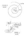
- Figure 1 is a diagram of an apparatus 10 for reading data prerecorded on an optical disk 12.
- the disk 12 is rotated by a disk servo 14 comprising a precisely controllable DC motor.
- a laser 16 irradiates the surface of the disk 12, and light reflected from the disk impinges on the surface of a detector 18.
- An optical head 20, located between the disk 12 and laser/detector 16, 18, is positioned by another servo (not shown) to read data from a desired track.
- Writing is carried out using similar optics, with the optical medium being preheated to enable light from laser 16 to form surface marks corresponding to data.
- the servos and laser/detector are controlled by a processor unit 22.
- apparatus 10 shown in Figure 1 typically are arranged within a common housing, such as provided by SCSI (Small Computer System Interface) resident at a personal computer or other computer requiring storage of a large quantity of data.
- SCSI Small Computer System Interface
- Data read and write logic implemented by processor unit 22 in the representative illustration of Figure 1, has been carried out by commercially available special function integrated circuits, such as the AM95C96 optical disk controller (ODC), manufactured by Advanced Micro Devices of Sunnyvale, California.
- ODC optical disk controller
- a system implementing the AM95C96, shown in Figure 2 comprises ODC 24 reading data through an encoder/decoder (ODE) 28 and a phase locked loop (PLL) 30 off the optical disk and writing to the optical disk.
- ODC optical disk controller
- PLL phase locked loop
- a CPU 32 controls seeking to the desired location on the disk.
- the ODC/ODE 24, 28 interfaces with CPU 32, working memory 34 and a disk interface 36 to process the applied data signals and transfer commands for compliance with particular specifications such as the X3B11 continuous composite servo (CCS), WORM/ERASABLE optical format developed by ANSI.
- CCS continuous composite servo
- WORM/ERASABLE optical format developed by ANSI.
- the ODC 24 is interfaced to a system bus by host interface unit 38, and is supported by buffer memory 40 and error processor 42. General operation of the system shown in Figure 2, being known to the prior art, is not described in detail.
- Figure 3 depicts the layout of tracks on an optical disk.
- the tracks are arranged along a spiral path on the surface of the disk 12, with each turn of the spiral being treated as a separate track.
- the optical disk may be 90mm in diameter, and may contain 10,000 tracks (numbered 0-9999 in Figure 3); each track is divided into twenty-five (25) sectors. Each sector in turn will carry 725 bytes of unformatted data.
- the optical disk in this example is capable of storing 181,250,000 bytes of data, or about 100,000 pages of text. Modifications include implementing more densely packed sectors, larger diameter disks and/or double- sided storage for enhanced information storage capacity.
- Figure 4 is a field diagram of the X3B11 format, comprising a header area that is "pre-stamped", followed by a data area for receiving data for storage.
- the first field of the header is a sector mark (SM) having a special redundant pattern. This field identifies the start of a sector.
- SM sector mark
- ODE 26 detects sector mark (SM) once within each sector.
- SM sector mark
- the sector mark comprises 80 bits arranged as a long burn followed by a transition pattern.
- Sector mark decoding is carried out by monitoring the long burn pattern of the track, and identifying a pattern characteristic of the sector mark.
- Detection of the sector mark pattern is a prerequisite to the reading of data from the corresponding sector. It identifies the region of each sector from which data is to be read because the data field is displaced from the sector mark by a defined number of bytes depending upon the particular standard involved. For example, in conventional X3B11 format, shown symbolically in Figure 4, the pre-stamped, or read only (RO), region extends 47 bytes beyond the sector mark field SM, followed by a magneto-optic region (MO) upon which data can be written once (the MO region is also termed a "WORM", or write once- read many, region).
- the data region of a 90mm, 512 byte sector size by convention follows the RO region by ODF and GAP bytes.
- the next sector mark field follows the data field by a buffer region of 13 bytes for timing margins.
- a "sync found" signal is generated by the ODE and the incoming data stream is decoded one block at a time while data synchronization between the data and decoder is maintained by alignment to the resync marks.
- Circuit delay is relatively high as a result of the additional length of signal paths that must be traversed between chips during handshaking and other communications.
- the pair of chips necessitates microprocessor address, data and control pins to transfer data and instructions between the chips.
- a high pin count diminishes the versitility of the controller by prohibiting the addition of new functions, such as diagnostics, requiring user access through the pins.
- the ODC reference clock termed RDREF, provided to the ODC 24
- PLL phase locked loop
- the timing signal will become unstable and the ODC has a tendency to "lock up.”
- delays in signal transfer inherent in separate chip architecture can cause X3B11 disk format incompatability or operation failure. If a command to abort a disk operation is asserted by the ODE, signal transfer protocol that must be exchanged between its internal processor and an external, main sequencer resident with the ODC, may cause the abort to be fully implemented too late.
- an integrated optical data disk controller comprises, on a common semiconductor substrate, (1) optical encoder/decoder (ODE) circuitry for finding reference marks and decoding data from a bit stream taken from an optical data disk and for encoding and supplying data to the disk, and (2) optical data controller (ODC) circuitry interconnected with the ODE and a host interface and providing disk read/write data and control signals to an external disk drive unit and (3) signal flow paths for transferring signals between the ODC and ODE.
- ODE optical encoder/decoder
- ODC optical data controller
- the ODE includes means for generating internal signals corresponding to the reference marks found on the disk, and at least one output pin, transfers these marks found signals outside the ODC/ODE substrate.
- the marks found signals preferrably are superimposed on a common output pin.
- the ODC and ODE functions can be immediately aborted, or disk drive operation appropriately modified, in response to particular controller or disk media characteristics including defective media indicated by these internal signals together with status/interrupt signals provided to ODE registers in the controller.
- the ODC circuit includes a data section storing ODE commands for controlling functions of the ODE circuit.
- External pins are coupled to the data section for reading the ODE commands issued by the ODC to the ODE.
- the ODE circuit is provided with window control logic for establishing windows of predefined sizes for searching disk sectors to find various reference marks.
- the data section of the ODC circuit stores data predefining the search window sizes.
- the ODE circuit includes synchronization logic means responsive to sync and resync signals developed by the ODE circuit for supplying decoded data from the disk to the ODC.
- a crystal-controlled clock provides a source of synchronization to the ODC and synchronization logic means.
- optical encoder/decoder circuitry for detecting reference marks and decoding data taken from said disk and for encoding and supplying data to the disk together with optical data controller (ODC) circuitry interconnected with the ODE and a host interface.
- ODE optical encoder/decoder
- external pins are coupled to the data section for enabling a user to monitor the ODC commands.
- the invention further provides availability of additional circuit pins for user diagnostics.
- X3B11 specification marks that is, sector mark, sync and resync, are supplied to a new "marks found" pin where the various marks can be distinguished from one another on the pin based upon differences in length and position.
- Another advantage is in common integration of programming for the ODC and ODE functions and availability of ODE command signals on a new set of "command" pins available to the user for diagnostics and debugging. Operation of the controller optionally can be aborted based upon information obtained from the status flags sent to a main sequencer of the controller chip. Abort is immediately carried out because the additional stages of abort operation necessary when internal and external (main sequencer) micor- processors must communicate with each other in the separate chip architecture is avoided.
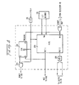
- IODC 100 comprises ODC and ODE regions 102, 104 depicted in the Figure as being isolated in separate portions of the chip but in practice may be arranged differently based upon circuit layout constraints.
- ODC 102 is similar to ODC 24 of the prior art, although programmed slightly differently and modified somewhat to accommodate new signals developed by the ODE 104; however, the ODE 104 has been modified considerably from the counterpart prior art ODE 28.
- ODE 104 contains five principal functional circuits in addition to a FIFO and synchronization logic unit 108 to be described later with reference to Figure 8.
- Marks detection circuits 110, 112 detect the various byte patterns or marks forming references on the sectors read from the tracks of an optical data disk.
- Mark detection and media control logic circuit 112 receives raw data from the disk, searches for the sector mark pattern provided by X3B11 specifications in the preferred embodiment, and supplies a sector mark found (SMF) signal to one input each of logic OR gates 113 and 115.
- SMF sector mark found
- the remaining input of logic OR gate 115 receives the output of AND gate 111 whose inputs comprise the sector mark found signal (SMF) from circuit 112 and a user selected pseudo sector mark enable signal (PSME) from ODE registers 130 in ODC 102.
- SMF sector mark found signal
- PSME pseudo sector mark enable signal
- the sector mark detection and media control logic circuit 112 is synchronized to an external constant reference clock (2FCLK) that operates at twice the frequency as that of ODC 102 (a requirement of NRZ/RLL 2,7 encoding and decoding), that is, at the frequency of a RDREF clock for timing ODC 102.
- 2FCLK an external constant reference clock
- gate 113 The output of gate 113 is supplied to one input of OR logic gate 114, the remaining input of which receives an address mark/sync found signal developed by circuit 110 and supplied through logic circuit 108 when the corresponding reference marks read from the disk are detected.
- Marks detection circuit 110 detects patterns of data taken from each sector to identify the presence of the address marks (AM), sync, resyncs (RS) and flag (flag detection is synchronized to 2FCLK). Flag pattern detection is described in detail in copending application US Serial No 810575, entitled “Repetitive Pattern Detection", also filed on even date herewith and incorporated herein by reference.
- Circuit 110 receives DATIN, which is a synchronized encoded data input received from an external phase locked loop (PLL) 123 of Figure 7. This data containing RLL data as well as the AM, sync, resyncs and VFO patterns taken directly from the disk, is synchronized to a clock SYNCLK provided by the PLL. Also supplied to circuit 110 is flag data (FLGDAT) providing flag detection obtained from encoded disk data.
- DATIN is a synchronized encoded data input received from an external phase locked loop (PLL) 123 of Figure 7.
- PLL phase locked loop
- FLGDAT flag data
- Address marks found or sync marks found by marks detection circuit 110 supplied to logic OR gate 114 are also applied to one input of logic OR gate 116.
- a signal provided to the other input of gate 116 by marks detection circuit 110 through logic circuit 108 indicates that a resync has been found.
- the output of logic OR gate 114 designating either that a sector mark, address mark or sync mark has been found, is supplied to a data section 118 of ODC 102 to enable sector data to be stored and transferred to a host bus.
- the reference mark found signals namely, sector mark found (SMF), pseudo sector mark (PSM), address mark found (AMF), sync found (SYNCF), pseudo sync found (PSYNCF), resync found (RSF) and flag found (FF) signals developed by the ODE circuit 104, together with the X3B11 specification, are shown in Figures 6(a)-(h).
- the output of gate 116 is supplied to a new output pin MKF (Marks Found) for diagnostics.
- MKF Marks Found
- This new output pin is made possible as a result of common integration of ODC 102, ODE 104 making available pins previously dedicated to microprocessor address, data and control lines, necessary for separate chips.
- the MKF pin is one of several diagnostic pins in group 128 of Figure 5 that enables the operation of the controller 100 to be monitored, and new disk drive control signals developed in response to particular conditions reflected by the marks found signals on the pin.
- a package for housing the controller (IODC) 100 and diagnostic pins 128 is shown in Figure 7.
- the various reference mark found signals, AM found, sync found and resync found, superimposed on the MKF pin, are distinguishable from each other by differences in byte length and position, as is apparent from the timing diagram of Figures 6(d), 6(e) and 6(g).
- the positions of AM found and sync found signals have a predefined relationship; the byte length (single byte per X3B11 specifications) of the resync found signal is less than that of the others.
- Window control logic circuit 120 controls the size of the resync mark detection window in accordance with an aspect of this invention.
- Other window sizes namely, those for detecting the sector mark, address mark, sync mark and flag are programmed in window controls store (WCS) unit 122 of ODC data section 108.
- WCS window controls store
- RLL decoder 124 receives DATIN from the disk, synchronized to SYNCLK, and converts the disk sector data from RLL 2,7 to NRZ data for supply to the FIFO and synchronization logic circuit 108.
- the circuit 108 includes the FIFO for transferring NRZ output data to the ODC 102 and into the data section 108.
- the RLL encoder and marks generation circuit 126 receives data from the data section 118, carries out RLL 2,7 encoding and generates the various marks necessary for applying resync marks and resync bytes to the data field of each sector.
- Circuit 108 shown in more detail in Figure 8, comprises FIFO 200, which preferably is two bits wide by fourteen bits deep, having two input terminals IN1 and IN2, and two output terminals OUT1 and OUT2.
- NRZ data decoded from the disk by RLL decoder 124 is supplied to input terminal IN1 to establish one bit stream of the two by fourteen bit FIFO 200.
- the other input terminal IN2 of the FIFO receives, through an OR gate 208, AM/SYNC and resync (RS) found signals generated by marks detection circuit 110.
- the marks found signals from gate 208 accordingly are time multiplexed in the second bit stream of the FIFO 200.
- Writing of data into the two inputs of FIFO 200 to establish the two bit streams is synchronized to a "write" clock signal obtained from SYNCLK and divided down by a factor of two (the divider circuit for this purpose is not shown).
- Reading of data from the FIFO 200 in turn is synchronized a "read" clock signal obtained from 2FCLK and divided down by a factor of two by divider 123.
- the first bit stream comprising NRZ output data at OUT1 of the FIFO 200 is supplied to the data section 118 of ODC 102.
- the second bit stream at OUT2 is demultiplexed by decoder 206 and supplied to OR gates 114 and 116, as described previously.
- a counter 202 preset to a bit count corresponding to the displacement of a block of the X3B11 data section, in the preferred embodiment (120 or 160 bits for 15 or 20 byte data blocks) by RS bytes from marks detection circuit 110, is downcounted synchronously to RDCLK by NRZ bits appearing at the output of the FIFO.
- the output of gate 204 asserts REREF to inhibit further reading of NRZ data from the FIFO by controlling data serialization and deserialization within the ODC 102 in the same manner as the prior art ODC.
- ODC 102 shown in more detail in Figure 5A, and which is connected to the SCSI side of the controller, supplies data read from the disk by ODE 104 and synchronized to sync marks and resync bytes by circuit 108 together with window control logic 120 and window controls store 122 for storage in buffer and host memories.
- the external clock from which RDREF is derived is a stable source of timing signals, preferrably crystal controlled, and is independent of modes of operation of the controller, the ODC circuit will not "hang up.” Hang up occasionally occurs in the prior art counterpart controller of Figure 2 because it derives ODC timing from a phase locked loop having a tendency to unlock during sector data read operation under certain conditions such as a defect in the disk medium.
- Status bits developed by ODE 104 are stored in ODE registers 130 of the ODC 102.
- the identification (ID) of any sectors for which a sync mark was not found is stored in register 130.
- a CPU (not shown), interfaced to ODC 102, will respond to an interrupt generated by ODE 104 to scan the sector during the same pass through the sector or during a subsequent pass in a data recovery mode of operation described in detail in the copending US Patent application 813272 entitled "Recovery of Data from Optical Data Disk Sectors having Missing or Defective Synchronization Information," incorporated herein by reference.
- ODE commands for controlling operation of the ODE circuit 104 are stored in the write control store (WCS) of data section 118 in ODC circuit 102.
- the ODE commands preferrably stored in the form of a three bit long (0-2) ODE control field of a 48 bit WCS word including bits for controlling write and read gates, produce the ODE commands which control the generation and detection of the sector mark, address mark, sync mark, flag and data encode/decode.
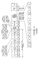
- the WCS word format and ODE commands are shown in tables II and III below.
- the ODE command bits are made externally available on output pins CMD (0-2) of pin group 128 for diagnostics and program debugging. When these pins are not used to carry ODE command bits, they can be defaulted to general pins (GENO (3-5).
- the IODC 100 incorporates a number of status flags that are supplied by ODE 104 to ODC 102 for storage in registers 130.
- the preferred embodiment provides twelve such status flags on two flag buses of seven and five flag lines, respectively.
- the group 128 of external pins in conjunction with the twelve status flag lines add quite a bit of flexibility to the controller 100, as they enable controller functions to be analyzed for debugging or other purposes such as to control a disk drive or to abort operation of the controller, if necessary, by an abort signal supplied to the ODC 102 by the ODE 104, as shown in Figure 5. It is apparent in this figure that abort is carried out immediately since additional layers of processing necessitated by processor circuits residing on separate chips of the prior art are eliminated.
- ODE circuits resides in data section 118 and main sequencer ( Figure 5A) of the ODC. Because there is no necessity to transfer signals between chips, speed of operation of the controller is improved, and interchip signal driving and buffering circuitry is eliminated. Of particular utility, additional pins made available by elimination of redundant pin functions enables diagnostics and debugging to be performed, both by the user and by a factory prior to product shipment.
Abstract
Description
- This invention relates generally to optical data disk drive controllers, and more particularly to a novel controller having optical disk controller (ODC) and optical data encoder-decoder (ODE) functions integrated on a common integrated circuit substrate.
- Optical disk media are capable of storing a considerable amount of data in the form of small marks or holes in the surface of the disk, each representing a bit of data. The marks, burned into the surface of the disk by a laser, are arranged along spiral tracks, each divided into a number of sectors.
- Figure 1 is a diagram of an
apparatus 10 for reading data prerecorded on anoptical disk 12. Thedisk 12 is rotated by adisk servo 14 comprising a precisely controllable DC motor. Alaser 16 irradiates the surface of thedisk 12, and light reflected from the disk impinges on the surface of adetector 18. Anoptical head 20, located between thedisk 12 and laser/detector laser 16 to form surface marks corresponding to data. The servos and laser/detector are controlled by aprocessor unit 22. - The
components comprising apparatus 10 shown in Figure 1 typically are arranged within a common housing, such as provided by SCSI (Small Computer System Interface) resident at a personal computer or other computer requiring storage of a large quantity of data. - Data read and write logic, implemented by
processor unit 22 in the representative illustration of Figure 1, has been carried out by commercially available special function integrated circuits, such as the AM95C96 optical disk controller (ODC), manufactured by Advanced Micro Devices of Sunnyvale, California. A system implementing the AM95C96, shown in Figure 2, comprisesODC 24 reading data through an encoder/decoder (ODE) 28 and a phase locked loop (PLL) 30 off the optical disk and writing to the optical disk. ACPU 32 controls seeking to the desired location on the disk. The ODC/ODE CPU 32,working memory 34 and adisk interface 36 to process the applied data signals and transfer commands for compliance with particular specifications such as the X3B11 continuous composite servo (CCS), WORM/ERASABLE optical format developed by ANSI. - The ODC 24 is interfaced to a system bus by
host interface unit 38, and is supported bybuffer memory 40 anderror processor 42. General operation of the system shown in Figure 2, being known to the prior art, is not described in detail. - Figure 3 depicts the layout of tracks on an optical disk. The tracks are arranged along a spiral path on the surface of the
disk 12, with each turn of the spiral being treated as a separate track. In one example, the optical disk may be 90mm in diameter, and may contain 10,000 tracks (numbered 0-9999 in Figure 3); each track is divided into twenty-five (25) sectors. Each sector in turn will carry 725 bytes of unformatted data. The optical disk in this example is capable of storing 181,250,000 bytes of data, or about 100,000 pages of text. Modifications include implementing more densely packed sectors, larger diameter disks and/or double- sided storage for enhanced information storage capacity. - Figure 4 is a field diagram of the X3B11 format, comprising a header area that is "pre-stamped", followed by a data area for receiving data for storage. The first field of the header is a sector mark (SM) having a special redundant pattern. This field identifies the start of a sector. The SM field as well as the other fields constituting the X3B11 format is summarized below in Table I.
-

- During both reading and writing operations, ODE 26 detects sector mark (SM) once within each sector. Referring to Table I, the sector mark comprises 80 bits arranged as a long burn followed by a transition pattern. Sector mark decoding is carried out by monitoring the long burn pattern of the track, and identifying a pattern characteristic of the sector mark.
- Detection of the sector mark pattern is a prerequisite to the reading of data from the corresponding sector. It identifies the region of each sector from which data is to be read because the data field is displaced from the sector mark by a defined number of bytes depending upon the particular standard involved. For example, in conventional X3B11 format, shown symbolically in Figure 4, the pre-stamped, or read only (RO), region extends 47 bytes beyond the sector mark field SM, followed by a magneto-optic region (MO) upon which data can be written once (the MO region is also termed a "WORM", or write once- read many, region). The data region of a 90mm, 512 byte sector size by convention follows the RO region by ODF and GAP bytes. The next sector mark field follows the data field by a buffer region of 13 bytes for timing margins.
- Another prerequisite of reading data from the disk is byte and bit alignment of data taken off each sector for decoding. In the X3B11 specification shown in Figure 4, a synchronization (sync) mark of 3 bytes, signifying the start of the sector data field, follows VF03. There are also several re-synchronization (resync) marks of one byte each at regular intervals to ensure byte alignment throughout a read operation. Following a successful header operation, the VF03 field is searched for presence of the sync mark. Upon detection of the sync mark, a "sync found" signal is generated by the ODE and the incoming data stream is decoded one block at a time while data synchronization between the data and decoder is maintained by alignment to the resync marks.
- Although the necessary functions are carried out by the prior art controller of Figure 2, integraton of the principal components, the
ODC 24 andODE 28, on separate integrated circuit "chips" is disadvantegeous in several respects. - First, because there is duplication of "intelligence" on the ODC and ODE chips and incorporation of additional interface circuitry to establish compatability between the chips, circuit and pattern layout complexity is considerable. Circuit delay is relatively high as a result of the additional length of signal paths that must be traversed between chips during handshaking and other communications.
- In addition, the pair of chips necessitates microprocessor address, data and control pins to transfer data and instructions between the chips. A high pin count diminishes the versitility of the controller by prohibiting the addition of new functions, such as diagnostics, requiring user access through the pins.
- Separate chip architecture also possesses other deficiencies inherent to internal operation of the controller. For example, in the prior art controller of Figure 2, during reading of the data field, the ODC reference clock, termed RDREF, provided to the
ODC 24, is derived from the phase locked loop (PLL) 30. When the loop becomes unlocked, for example as a result of a defect in the medium, the timing signal will become unstable and the ODC has a tendency to "lock up." As another example, delays in signal transfer inherent in separate chip architecture can cause X3B11 disk format incompatability or operation failure. If a command to abort a disk operation is asserted by the ODE, signal transfer protocol that must be exchanged between its internal processor and an external, main sequencer resident with the ODC, may cause the abort to be fully implemented too late. - The above and other deficiencies of the prior art are addressed in the invention by implementing ODC and ODE functions on a common chip. More specifically, an integrated optical data disk controller, in accordance with one aspect of the invention, comprises, on a common semiconductor substrate, (1) optical encoder/decoder (ODE) circuitry for finding reference marks and decoding data from a bit stream taken from an optical data disk and for encoding and supplying data to the disk, and (2) optical data controller (ODC) circuitry interconnected with the ODE and a host interface and providing disk read/write data and control signals to an external disk drive unit and (3) signal flow paths for transferring signals between the ODC and ODE.
- Preferably, the ODE includes means for generating internal signals corresponding to the reference marks found on the disk, and at least one output pin, transfers these marks found signals outside the ODC/ODE substrate. The marks found signals preferrably are superimposed on a common output pin. The ODC and ODE functions can be immediately aborted, or disk drive operation appropriately modified, in response to particular controller or disk media characteristics including defective media indicated by these internal signals together with status/interrupt signals provided to ODE registers in the controller.
- Preferably, the ODC circuit includes a data section storing ODE commands for controlling functions of the ODE circuit. External pins are coupled to the data section for reading the ODE commands issued by the ODC to the ODE.
- Preferably the ODE circuit is provided with window control logic for establishing windows of predefined sizes for searching disk sectors to find various reference marks. Preferrably, the data section of the ODC circuit stores data predefining the search window sizes.
- In another aspect, the ODE circuit includes synchronization logic means responsive to sync and resync signals developed by the ODE circuit for supplying decoded data from the disk to the ODC. A crystal-controlled clock provides a source of synchronization to the ODC and synchronization logic means.
- Another aspect of the invention provides optical encoder/decoder (ODE) circuitry for detecting reference marks and decoding data taken from said disk and for encoding and supplying data to the disk together with optical data controller (ODC) circuitry interconnected with the ODE and a host interface.
- Preferrably, external pins are coupled to the data section for enabling a user to monitor the ODC commands.
- Integration of the ODC and ODE functions as described shares circuit functions, reducing the amount of circuitry required to be implemented on the chip and increasing the speed of signal processing. The invention further provides availability of additional circuit pins for user diagnostics. For example, X3B11 specification marks, that is, sector mark, sync and resync, are supplied to a new "marks found" pin where the various marks can be distinguished from one another on the pin based upon differences in length and position.
- Another advantage is in common integration of programming for the ODC and ODE functions and availability of ODE command signals on a new set of "command" pins available to the user for diagnostics and debugging. Operation of the controller optionally can be aborted based upon information obtained from the status flags sent to a main sequencer of the controller chip. Abort is immediately carried out because the additional stages of abort operation necessary when internal and external (main sequencer) micor- processors must communicate with each other in the separate chip architecture is avoided.
- Still other objects and advantages of the present invention will become readily apparent to those skilled in this art from the following detailed description, wherein only the preferred embodiment of the invention is shown and described, simply by way of illustration of the best mode contemplated of carrying out the invention. As will be realized, the invention is capable of other and different embodiments, and its several details are capable of modifications in various obvious respects, all without departing from the invention. Accordingly, the drawing and description are to be regarded as illustrative in nature, and not as restrictive.
-
- Figure 1 is a simplified diagram of an optical disk read/write system within which the present invention may be implemented.
- Figure 2 is a diagram of an optical disk controller system of the prior art comprising separate ODC and ODE chips.
- Figure 3 is a diagram showing a track format of an optical data disk.
- Figure 4 is a diagram showing X3B11 data format utilized in the preferred embodiment.
- Figure 5 is a block diagram of a optical disk controller having integrated ODC and ODE functions in accordance with the invention.
- Figure 5A is a more detailed diagram of the ODC of Figure 5.
- Figures 6(a)-(h) show timing relationships among reference mark signals produced by the controller.
- Figure 7 shows how the integrated ODC/ODE system of the invention is interconnected to timing reference sources and a disk drive unit.
- Figure 8 is a detailed diagram of the FIFO and synchronization logic circuit of Figure 5.
- The invention is implemented by circuitry shown in Figure 5 with optical disk controller (ODC) and optical data encoder-decoder (ODE) functions on a common semiconductor substrate (chip) 101 to form an integrated optical integrated optical disk controller (IODC) 100.
IODC 100 comprises ODC andODE regions ODC 102 is similar toODC 24 of the prior art, although programmed slightly differently and modified somewhat to accommodate new signals developed by theODE 104; however, theODE 104 has been modified considerably from the counterpartprior art ODE 28. -
ODE 104 contains five principal functional circuits in addition to a FIFO andsynchronization logic unit 108 to be described later with reference to Figure 8.Marks detection circuits control logic circuit 112 receives raw data from the disk, searches for the sector mark pattern provided by X3B11 specifications in the preferred embodiment, and supplies a sector mark found (SMF) signal to one input each of logic ORgates gate 115 receives the output of AND gate 111 whose inputs comprise the sector mark found signal (SMF) fromcircuit 112 and a user selected pseudo sector mark enable signal (PSME) fromODE registers 130 inODC 102. To the remaining input ofgate 113 is applied a psuedo sector mark signal developed bycircuit 112. Details on sector mark detection and generation of the sector mark found and pseudo sector mark signals are given in copending US Patent applications Serial No 810576 for "Sector Mark Pattern Detection for Optical Disk Controller" and USSN 810574 for "Sector Mark Detection in Long Burn Pattern for Optical Data Disks," both incorporated by reference. - The sector mark detection and media
control logic circuit 112 is synchronized to an external constant reference clock (2FCLK) that operates at twice the frequency as that of ODC 102 (a requirement of NRZ/RLL ODC 102. - The output of
gate 113 is supplied to one input of ORlogic gate 114, the remaining input of which receives an address mark/sync found signal developed bycircuit 110 and supplied throughlogic circuit 108 when the corresponding reference marks read from the disk are detected. -
Marks detection circuit 110 detects patterns of data taken from each sector to identify the presence of the address marks (AM), sync, resyncs (RS) and flag (flag detection is synchronized to 2FCLK). Flag pattern detection is described in detail in copending application US Serial No 810575, entitled "Repetitive Pattern Detection", also filed on even date herewith and incorporated herein by reference.Circuit 110 receives DATIN, which is a synchronized encoded data input received from an external phase locked loop (PLL) 123 of Figure 7. This data containing RLL data as well as the AM, sync, resyncs and VFO patterns taken directly from the disk, is synchronized to a clock SYNCLK provided by the PLL. Also supplied tocircuit 110 is flag data (FLGDAT) providing flag detection obtained from encoded disk data. - Address marks found or sync marks found by
marks detection circuit 110 supplied to logic ORgate 114 are also applied to one input of logic ORgate 116. A signal provided to the other input ofgate 116 bymarks detection circuit 110 throughlogic circuit 108 indicates that a resync has been found. - The output of logic OR
gate 114, designating either that a sector mark, address mark or sync mark has been found, is supplied to adata section 118 ofODC 102 to enable sector data to be stored and transferred to a host bus. The reference mark found signals, namely, sector mark found (SMF), pseudo sector mark (PSM), address mark found (AMF), sync found (SYNCF), pseudo sync found (PSYNCF), resync found (RSF) and flag found (FF) signals developed by theODE circuit 104, together with the X3B11 specification, are shown in Figures 6(a)-(h). - The output of
gate 116, corresponding to address mark, sync mark and resync mark found signals, is supplied to a new output pin MKF (Marks Found) for diagnostics. This new output pin is made possible as a result of common integration ofODC 102,ODE 104 making available pins previously dedicated to microprocessor address, data and control lines, necessary for separate chips. The MKF pin is one of several diagnostic pins ingroup 128 of Figure 5 that enables the operation of thecontroller 100 to be monitored, and new disk drive control signals developed in response to particular conditions reflected by the marks found signals on the pin. A package for housing the controller (IODC) 100 anddiagnostic pins 128 is shown in Figure 7. - The various reference mark found signals, AM found, sync found and resync found, superimposed on the MKF pin, are distinguishable from each other by differences in byte length and position, as is apparent from the timing diagram of Figures 6(d), 6(e) and 6(g). For example, the positions of AM found and sync found signals have a predefined relationship; the byte length (single byte per X3B11 specifications) of the resync found signal is less than that of the others.
- Window
control logic circuit 120 controls the size of the resync mark detection window in accordance with an aspect of this invention. Other window sizes, namely, those for detecting the sector mark, address mark, sync mark and flag are programmed in window controls store (WCS)unit 122 ofODC data section 108. -
RLL decoder 124 receives DATIN from the disk, synchronized to SYNCLK, and converts the disk sector data fromRLL synchronization logic circuit 108. Thecircuit 108 includes the FIFO for transferring NRZ output data to theODC 102 and into thedata section 108. The RLL encoder and marksgeneration circuit 126 receives data from thedata section 118, carries outRLL -
Circuit 108, shown in more detail in Figure 8, comprisesFIFO 200, which preferably is two bits wide by fourteen bits deep, having two input terminals IN1 and IN2, and two output terminals OUT1 and OUT2. NRZ data decoded from the disk byRLL decoder 124 is supplied to input terminal IN1 to establish one bit stream of the two by fourteenbit FIFO 200. The other input terminal IN2 of the FIFO receives, through an ORgate 208, AM/SYNC and resync (RS) found signals generated bymarks detection circuit 110. The marks found signals fromgate 208 accordingly are time multiplexed in the second bit stream of theFIFO 200. - Writing of data into the two inputs of
FIFO 200 to establish the two bit streams is synchronized to a "write" clock signal obtained from SYNCLK and divided down by a factor of two (the divider circuit for this purpose is not shown). Reading of data from theFIFO 200 in turn is synchronized a "read" clock signal obtained from 2FCLK and divided down by a factor of two bydivider 123. - The first bit stream comprising NRZ output data at OUT1 of the
FIFO 200 is supplied to thedata section 118 ofODC 102. The second bit stream at OUT2 is demultiplexed bydecoder 206 and supplied to ORgates - A
counter 202, preset to a bit count corresponding to the displacement of a block of the X3B11 data section, in the preferred embodiment (120 or 160 bits for 15 or 20 byte data blocks) by RS bytes frommarks detection circuit 110, is downcounted synchronously to RDCLK by NRZ bits appearing at the output of the FIFO. When thecounter 202 has downcounted to zero. the output ofgate 204 asserts REREF to inhibit further reading of NRZ data from the FIFO by controlling data serialization and deserialization within theODC 102 in the same manner as the prior art ODC. -
ODC 102, shown in more detail in Figure 5A, and which is connected to the SCSI side of the controller, supplies data read from the disk byODE 104 and synchronized to sync marks and resync bytes bycircuit 108 together withwindow control logic 120 and window controls store 122 for storage in buffer and host memories. Because the external clock from which RDREF is derived is a stable source of timing signals, preferrably crystal controlled, and is independent of modes of operation of the controller, the ODC circuit will not "hang up." Hang up occasionally occurs in the prior art counterpart controller of Figure 2 because it derives ODC timing from a phase locked loop having a tendency to unlock during sector data read operation under certain conditions such as a defect in the disk medium. - Status bits developed by
ODE 104 are stored in ODE registers 130 of theODC 102. As one example, in a data recovery mode of operation that takes place when a sync mark is not found, the identification (ID) of any sectors for which a sync mark was not found is stored inregister 130. A CPU (not shown), interfaced toODC 102, will respond to an interrupt generated byODE 104 to scan the sector during the same pass through the sector or during a subsequent pass in a data recovery mode of operation described in detail in the copending US Patent application 813272 entitled "Recovery of Data from Optical Data Disk Sectors having Missing or Defective Synchronization Information," incorporated herein by reference. - In accordance with an important aspect of the invention, ODE commands for controlling operation of the
ODE circuit 104 are stored in the write control store (WCS) ofdata section 118 inODC circuit 102. The ODE commands, preferrably stored in the form of a three bit long (0-2) ODE control field of a 48 bit WCS word including bits for controlling write and read gates, produce the ODE commands which control the generation and detection of the sector mark, address mark, sync mark, flag and data encode/decode. The WCS word format and ODE commands are shown in tables II and III below.

- The ODE command bits are made externally available on output pins CMD (0-2) of
pin group 128 for diagnostics and program debugging. When these pins are not used to carry ODE command bits, they can be defaulted to general pins (GENO (3-5). - The
IODC 100 incorporates a number of status flags that are supplied byODE 104 toODC 102 for storage inregisters 130. The preferred embodiment provides twelve such status flags on two flag buses of seven and five flag lines, respectively. - The
group 128 of external pins in conjunction with the twelve status flag lines add quite a bit of flexibility to thecontroller 100, as they enable controller functions to be analyzed for debugging or other purposes such as to control a disk drive or to abort operation of the controller, if necessary, by an abort signal supplied to theODC 102 by theODE 104, as shown in Figure 5. It is apparent in this figure that abort is carried out immediately since additional layers of processing necessitated by processor circuits residing on separate chips of the prior art are eliminated. - Accordingly, numerous advantages and improvements in operation of an optical data disk controller are ODE circuits resides in
data section 118 and main sequencer (Figure 5A) of the ODC. Because there is no necessity to transfer signals between chips, speed of operation of the controller is improved, and interchip signal driving and buffering circuitry is eliminated. Of particular utility, additional pins made available by elimination of redundant pin functions enables diagnostics and debugging to be performed, both by the user and by a factory prior to product shipment. - In this disclosure, there is shown and described only the preferred embodiment of the invention, but, as aforementioned, it is to be understood that the invention is capable of use in various other combinations and environments and is capable of changes or modifications within the scope of the inventive concept as expressed herein.
Claims (15)
Applications Claiming Priority (2)
| Application Number | Priority Date | Filing Date | Title |
|---|---|---|---|
| US81327591A | 1991-12-24 | 1991-12-24 | |
| US813275 | 1991-12-24 |
Publications (2)
| Publication Number | Publication Date |
|---|---|
| EP0549152A2 true EP0549152A2 (en) | 1993-06-30 |
| EP0549152A3 EP0549152A3 (en) | 1993-12-08 |
Family
ID=25211948
Family Applications (1)
| Application Number | Title | Priority Date | Filing Date |
|---|---|---|---|
| EP19920310962 Ceased EP0549152A3 (en) | 1991-12-24 | 1992-12-01 | Single chip controller for optical data disk drives |
Country Status (4)
| Country | Link |
|---|---|
| US (1) | US5559983A (en) |
| EP (1) | EP0549152A3 (en) |
| JP (1) | JPH05298701A (en) |
| KR (1) | KR930014372A (en) |
Families Citing this family (14)
| Publication number | Priority date | Publication date | Assignee | Title |
|---|---|---|---|---|
| US5737371A (en) * | 1995-12-06 | 1998-04-07 | International Business Machines Corporation | Realignment of data stream from an optical disk |
| US6282045B1 (en) * | 1997-09-15 | 2001-08-28 | Texas Instruments Incorporated | Server hard disk drive integrated circuit and method of operation |
| US6456213B1 (en) | 1998-06-11 | 2002-09-24 | Seagate Technology Llc | Digitizing readback waveform for testing hard disc drives |
| US6167551A (en) * | 1998-07-29 | 2000-12-26 | Neomagic Corp. | DVD controller with embedded DRAM for ECC-block buffering |
| US6158040A (en) * | 1998-07-29 | 2000-12-05 | Neomagic Corp. | Rotated data-aligmnent in wade embedded DRAM for page-mode column ECC in a DVD controller |
| JP2002531883A (en) * | 1998-11-09 | 2002-09-24 | サーラスロジック、アイ・エヌ・シー | Mixed signal single chip integrated system electronics for magnetic hard disk drives. |
| JP2000324077A (en) * | 1999-05-07 | 2000-11-24 | Nec Ic Microcomput Syst Ltd | Byte arraying and frame synchronizing device |
| US8361587B2 (en) * | 2007-07-31 | 2013-01-29 | Nbcuniversal Media, Llc | Enhanced security of optical article |
| US8229276B2 (en) * | 2007-09-28 | 2012-07-24 | Nbcuniversal Media, Llc | Limited play optical article |
| US8646106B2 (en) * | 2007-09-28 | 2014-02-04 | Nbcuniversal Media, Llc | Limited play optical article |
| US8051441B2 (en) * | 2008-03-31 | 2011-11-01 | Nbcuniversal Media, Llc | Player-readable code on optical media |
| US9514782B2 (en) * | 2008-05-13 | 2016-12-06 | Nbcuniversal Media, Llc | Method and system for activation of an optical article |
| US8488428B2 (en) | 2008-05-14 | 2013-07-16 | Nbcuniversal Media, Llc | Enhanced security of optical article |
| US8097324B2 (en) * | 2008-05-14 | 2012-01-17 | Nbcuniversal Media, Llc | Enhanced security of optical article |
Citations (8)
| Publication number | Priority date | Publication date | Assignee | Title |
|---|---|---|---|---|
| JPS58181162A (en) * | 1982-04-16 | 1983-10-22 | Hitachi Ltd | Information storage system |
| JPS6126975A (en) * | 1984-07-17 | 1986-02-06 | Mitsubishi Electric Corp | Optical disk controller |
| JPS62102483A (en) * | 1985-10-30 | 1987-05-12 | Hitachi Ltd | Optical disk format controller |
| US4800550A (en) * | 1986-07-03 | 1989-01-24 | Pioneer Electronic Corporation | Multi-format optical disk recording/reproducing system |
| WO1989006427A1 (en) * | 1988-01-06 | 1989-07-13 | Digital Equipment Corporation | Synchronization for stored data |
| US4862443A (en) * | 1986-02-28 | 1989-08-29 | Sharp Kabushiki Kaisha | Sync signal detection apparatus for accurately synchronizing reproduced data |
| GB2241803A (en) * | 1987-06-03 | 1991-09-11 | Sony Corp | Controlling data transfer for recording/reproduction. |
| US5187615A (en) * | 1988-03-30 | 1993-02-16 | Hitachi, Ltd. | Data separator and signal processing circuit |
Family Cites Families (6)
| Publication number | Priority date | Publication date | Assignee | Title |
|---|---|---|---|---|
| JPS5877034A (en) * | 1981-10-30 | 1983-05-10 | Hitachi Ltd | Controlling system for unrewritable storage device |
| JPS6050669A (en) * | 1983-08-29 | 1985-03-20 | Hitachi Ltd | Demodulating system of data |
| JPH0770173B2 (en) * | 1987-03-06 | 1995-07-31 | 松下電器産業株式会社 | Information recording / reproducing device |
| JP2732591B2 (en) * | 1988-06-30 | 1998-03-30 | 株式会社東芝 | Recording medium processing device |
| DE69113357T2 (en) * | 1990-07-30 | 1996-05-30 | Nec Corp | Plate control with format control unit, which directly enables a return operation. |
| US5235585A (en) * | 1991-09-11 | 1993-08-10 | International Business Machines | Reassigning defective sectors on a disk |
-
1992
- 1992-12-01 EP EP19920310962 patent/EP0549152A3/en not_active Ceased
- 1992-12-22 JP JP4342338A patent/JPH05298701A/en not_active Withdrawn
- 1992-12-24 KR KR1019920025474A patent/KR930014372A/en not_active Application Discontinuation
-
1994
- 1994-08-16 US US08/291,814 patent/US5559983A/en not_active Expired - Lifetime
Patent Citations (8)
| Publication number | Priority date | Publication date | Assignee | Title |
|---|---|---|---|---|
| JPS58181162A (en) * | 1982-04-16 | 1983-10-22 | Hitachi Ltd | Information storage system |
| JPS6126975A (en) * | 1984-07-17 | 1986-02-06 | Mitsubishi Electric Corp | Optical disk controller |
| JPS62102483A (en) * | 1985-10-30 | 1987-05-12 | Hitachi Ltd | Optical disk format controller |
| US4862443A (en) * | 1986-02-28 | 1989-08-29 | Sharp Kabushiki Kaisha | Sync signal detection apparatus for accurately synchronizing reproduced data |
| US4800550A (en) * | 1986-07-03 | 1989-01-24 | Pioneer Electronic Corporation | Multi-format optical disk recording/reproducing system |
| GB2241803A (en) * | 1987-06-03 | 1991-09-11 | Sony Corp | Controlling data transfer for recording/reproduction. |
| WO1989006427A1 (en) * | 1988-01-06 | 1989-07-13 | Digital Equipment Corporation | Synchronization for stored data |
| US5187615A (en) * | 1988-03-30 | 1993-02-16 | Hitachi, Ltd. | Data separator and signal processing circuit |
Non-Patent Citations (6)
| Title |
|---|
| DATABASE WPI Section EI, Week 9309, Derwent Publications Ltd., London, GB; Class T03, AN 93-075936 & US-A-5 187 615 (HITACHI LTD) * |
| PATENT ABSTRACTS OF JAPAN vol. 10, no. 180 (P-471)24 June 1986 & JP-A-61 026 975 ( MITSUBISHI ELECTRIC CORP. ) * |
| PATENT ABSTRACTS OF JAPAN vol. 11, no. 311 (P-625)12 October 1987 & JP-A-62 102 483 ( HITACHI LTD ) * |
| PATENT ABSTRACTS OF JAPAN vol. 16, no. 28 (P-1302)23 January 1992 & JP-A-32 40 821 ( CANON INC. ) 28 October 1991 * |
| PATENT ABSTRACTS OF JAPAN vol. 16, no. 39 (P-1305)30 January 1992 & JP-A-32 45 369 ( MATSUSHITA ELECTRIC IND. CO. LTD ) 31 October 1991 * |
| PATENT ABSTRACTS OF JAPAN vol. 8, no. 27 (P-252)4 February 1984 & JP-A-58 181 162 ( HITACHI SEISAKUSHO KK ) * |
Also Published As
| Publication number | Publication date |
|---|---|
| JPH05298701A (en) | 1993-11-12 |
| US5559983A (en) | 1996-09-24 |
| EP0549152A3 (en) | 1993-12-08 |
| KR930014372A (en) | 1993-07-23 |
Similar Documents
| Publication | Publication Date | Title |
|---|---|---|
| US5416760A (en) | Recovery of data from optical data disk sectors having missing or defective synchronization information | |
| US5559983A (en) | Single chip controller for optical data disk drives | |
| US5231545A (en) | Fault tolerant rll data sector address mark decoder | |
| US4375655A (en) | Universal digital data copying system | |
| US7099246B2 (en) | Method and apparatus for recording data on an optical disc with restarting writing of data after data recording interruption | |
| JPH03232165A (en) | Disc file or tape drive by high servo extraction speed | |
| JPH06267195A (en) | Disc-drive of redundant recording | |
| JPS5822831B2 (en) | Signal pattern detection circuit | |
| US5623477A (en) | Optical recording disk capable of resynchronization in digital encoding and decoding | |
| JPH0294070A (en) | Digital information reproducing device | |
| US4644418A (en) | Floppy disk control apparatus | |
| US5349350A (en) | Run length limited encoding/decoding system for low power disk drives | |
| KR100194025B1 (en) | Data Sector Configuration and Data Sector Timing Generator for High Capacity Hard Disk Drives | |
| US5351231A (en) | Programmable mark detection and windowing for optical disk controllers | |
| JPH0650591B2 (en) | FDD window gate circuit | |
| US5237552A (en) | Sector mark detection in long burn pattern for optical data disks | |
| US5444685A (en) | Sector mark pattern detection for optical data disk controller | |
| US6154331A (en) | Disk formatter write gate look-ahead device | |
| JP2571669B2 (en) | Optical drive controller, optical disk drive and information reading method | |
| KR100403289B1 (en) | Magnetic disk separately having defect occurrence information in servo area and magnetic disk device for detecting the same | |
| EP0549154A2 (en) | Repetitive pattern detection | |
| EP0549153B1 (en) | Sector mark detection for optical data disks | |
| JPS62239382A (en) | Method and device for optical disk recording and reproduction | |
| JPS634458A (en) | Information recording and reproducing device | |
| JPH0254445A (en) | Recorder and recording system for master disk |
Legal Events
| Date | Code | Title | Description |
|---|---|---|---|
| PUAI | Public reference made under article 153(3) epc to a published international application that has entered the european phase |
Free format text: ORIGINAL CODE: 0009012 |
|
| AK | Designated contracting states |
Kind code of ref document: A2 Designated state(s): AT BE CH DE DK ES FR GB GR IE IT LI LU NL PT SE |
|
| PUAL | Search report despatched |
Free format text: ORIGINAL CODE: 0009013 |
|
| AK | Designated contracting states |
Kind code of ref document: A3 Designated state(s): AT BE CH DE DK ES FR GB GR IE IT LI LU NL PT SE |
|
| 17P | Request for examination filed |
Effective date: 19940314 |
|
| 17Q | First examination report despatched |
Effective date: 19951228 |
|
| GRAG | Despatch of communication of intention to grant |
Free format text: ORIGINAL CODE: EPIDOS AGRA |
|
| STAA | Information on the status of an ep patent application or granted ep patent |
Free format text: STATUS: THE APPLICATION HAS BEEN REFUSED |
|
| 18R | Application refused |
Effective date: 19970720 |