EP0545787B1 - Semiconductor heterostructure for optical signal processing - Google Patents
Semiconductor heterostructure for optical signal processing Download PDFInfo
- Publication number
- EP0545787B1 EP0545787B1 EP92403193A EP92403193A EP0545787B1 EP 0545787 B1 EP0545787 B1 EP 0545787B1 EP 92403193 A EP92403193 A EP 92403193A EP 92403193 A EP92403193 A EP 92403193A EP 0545787 B1 EP0545787 B1 EP 0545787B1
- Authority
- EP
- European Patent Office
- Prior art keywords
- thin film
- well
- heterostructure
- band
- equal
- Prior art date
- Legal status (The legal status is an assumption and is not a legal conclusion. Google has not performed a legal analysis and makes no representation as to the accuracy of the status listed.)
- Expired - Lifetime
Links
- 239000004065 semiconductor Substances 0.000 title claims description 20
- 230000003287 optical effect Effects 0.000 title claims description 3
- 238000012545 processing Methods 0.000 title claims description 3
- 229910000673 Indium arsenide Inorganic materials 0.000 claims description 30
- RPQDHPTXJYYUPQ-UHFFFAOYSA-N indium arsenide Chemical compound [In]#[As] RPQDHPTXJYYUPQ-UHFFFAOYSA-N 0.000 claims description 30
- 238000010521 absorption reaction Methods 0.000 claims description 28
- 239000000463 material Substances 0.000 claims description 21
- 230000004888 barrier function Effects 0.000 claims description 15
- 230000005855 radiation Effects 0.000 claims description 6
- 239000010409 thin film Substances 0.000 claims 12
- 239000010408 film Substances 0.000 claims 3
- 239000010410 layer Substances 0.000 description 53
- 230000007704 transition Effects 0.000 description 41
- 229910001218 Gallium arsenide Inorganic materials 0.000 description 36
- 229910005542 GaSb Inorganic materials 0.000 description 24
- 229910017115 AlSb Inorganic materials 0.000 description 16
- 238000013459 approach Methods 0.000 description 7
- 230000007423 decrease Effects 0.000 description 7
- 238000000034 method Methods 0.000 description 7
- 230000005428 wave function Effects 0.000 description 7
- 238000003780 insertion Methods 0.000 description 6
- 230000037431 insertion Effects 0.000 description 6
- 230000000694 effects Effects 0.000 description 5
- 230000005670 electromagnetic radiation Effects 0.000 description 4
- 239000000758 substrate Substances 0.000 description 4
- 239000006185 dispersion Substances 0.000 description 3
- 238000006073 displacement reaction Methods 0.000 description 3
- 230000005684 electric field Effects 0.000 description 3
- 230000002745 absorbent Effects 0.000 description 2
- 239000002250 absorbent Substances 0.000 description 2
- 230000008901 benefit Effects 0.000 description 2
- 239000000969 carrier Substances 0.000 description 2
- 230000007246 mechanism Effects 0.000 description 2
- 239000013307 optical fiber Substances 0.000 description 2
- 230000005693 optoelectronics Effects 0.000 description 2
- 230000010287 polarization Effects 0.000 description 2
- 239000002356 single layer Substances 0.000 description 2
- 238000006467 substitution reaction Methods 0.000 description 2
- 101100004286 Caenorhabditis elegans best-5 gene Proteins 0.000 description 1
- 229910045601 alloy Inorganic materials 0.000 description 1
- 239000000956 alloy Substances 0.000 description 1
- 230000008859 change Effects 0.000 description 1
- 150000001875 compounds Chemical class 0.000 description 1
- 239000000470 constituent Substances 0.000 description 1
- 239000013078 crystal Substances 0.000 description 1
- 230000003247 decreasing effect Effects 0.000 description 1
- 238000000151 deposition Methods 0.000 description 1
- 230000008021 deposition Effects 0.000 description 1
- 230000005284 excitation Effects 0.000 description 1
- 239000000835 fiber Substances 0.000 description 1
- 239000011521 glass Substances 0.000 description 1
- 229910052738 indium Inorganic materials 0.000 description 1
- WPYVAWXEWQSOGY-UHFFFAOYSA-N indium antimonide Chemical compound [Sb]#[In] WPYVAWXEWQSOGY-UHFFFAOYSA-N 0.000 description 1
- APFVFJFRJDLVQX-UHFFFAOYSA-N indium atom Chemical group [In] APFVFJFRJDLVQX-UHFFFAOYSA-N 0.000 description 1
- 239000011159 matrix material Substances 0.000 description 1
- 229910052751 metal Inorganic materials 0.000 description 1
- 239000002184 metal Substances 0.000 description 1
- 239000000203 mixture Substances 0.000 description 1
- 238000001451 molecular beam epitaxy Methods 0.000 description 1
- 230000010363 phase shift Effects 0.000 description 1
- 238000005036 potential barrier Methods 0.000 description 1
- 230000008569 process Effects 0.000 description 1
- 230000005610 quantum mechanics Effects 0.000 description 1
- 230000006798 recombination Effects 0.000 description 1
- 238000005215 recombination Methods 0.000 description 1
- 238000011084 recovery Methods 0.000 description 1
- 230000009467 reduction Effects 0.000 description 1
- 238000009738 saturating Methods 0.000 description 1
- 230000003595 spectral effect Effects 0.000 description 1
- 230000007480 spreading Effects 0.000 description 1
- 238000013519 translation Methods 0.000 description 1
- 238000000927 vapour-phase epitaxy Methods 0.000 description 1
Images


Classifications
-
- B—PERFORMING OPERATIONS; TRANSPORTING
- B82—NANOTECHNOLOGY
- B82Y—SPECIFIC USES OR APPLICATIONS OF NANOSTRUCTURES; MEASUREMENT OR ANALYSIS OF NANOSTRUCTURES; MANUFACTURE OR TREATMENT OF NANOSTRUCTURES
- B82Y20/00—Nanooptics, e.g. quantum optics or photonic crystals
-
- G—PHYSICS
- G02—OPTICS
- G02F—OPTICAL DEVICES OR ARRANGEMENTS FOR THE CONTROL OF LIGHT BY MODIFICATION OF THE OPTICAL PROPERTIES OF THE MEDIA OF THE ELEMENTS INVOLVED THEREIN; NON-LINEAR OPTICS; FREQUENCY-CHANGING OF LIGHT; OPTICAL LOGIC ELEMENTS; OPTICAL ANALOGUE/DIGITAL CONVERTERS
- G02F1/00—Devices or arrangements for the control of the intensity, colour, phase, polarisation or direction of light arriving from an independent light source, e.g. switching, gating or modulating; Non-linear optics
- G02F1/01—Devices or arrangements for the control of the intensity, colour, phase, polarisation or direction of light arriving from an independent light source, e.g. switching, gating or modulating; Non-linear optics for the control of the intensity, phase, polarisation or colour
- G02F1/015—Devices or arrangements for the control of the intensity, colour, phase, polarisation or direction of light arriving from an independent light source, e.g. switching, gating or modulating; Non-linear optics for the control of the intensity, phase, polarisation or colour based on semiconductor elements with at least one potential jump barrier, e.g. PN, PIN junction
- G02F1/017—Structures with periodic or quasi periodic potential variation, e.g. superlattices, quantum wells
- G02F1/01725—Non-rectangular quantum well structures, e.g. graded or stepped quantum wells
-
- H—ELECTRICITY
- H01—ELECTRIC ELEMENTS
- H01L—SEMICONDUCTOR DEVICES NOT COVERED BY CLASS H10
- H01L31/00—Semiconductor devices sensitive to infrared radiation, light, electromagnetic radiation of shorter wavelength or corpuscular radiation and specially adapted either for the conversion of the energy of such radiation into electrical energy or for the control of electrical energy by such radiation; Processes or apparatus specially adapted for the manufacture or treatment thereof or of parts thereof; Details thereof
- H01L31/0248—Semiconductor devices sensitive to infrared radiation, light, electromagnetic radiation of shorter wavelength or corpuscular radiation and specially adapted either for the conversion of the energy of such radiation into electrical energy or for the control of electrical energy by such radiation; Processes or apparatus specially adapted for the manufacture or treatment thereof or of parts thereof; Details thereof characterised by their semiconductor bodies
- H01L31/0352—Semiconductor devices sensitive to infrared radiation, light, electromagnetic radiation of shorter wavelength or corpuscular radiation and specially adapted either for the conversion of the energy of such radiation into electrical energy or for the control of electrical energy by such radiation; Processes or apparatus specially adapted for the manufacture or treatment thereof or of parts thereof; Details thereof characterised by their semiconductor bodies characterised by their shape or by the shapes, relative sizes or disposition of the semiconductor regions
-
- G—PHYSICS
- G02—OPTICS
- G02F—OPTICAL DEVICES OR ARRANGEMENTS FOR THE CONTROL OF LIGHT BY MODIFICATION OF THE OPTICAL PROPERTIES OF THE MEDIA OF THE ELEMENTS INVOLVED THEREIN; NON-LINEAR OPTICS; FREQUENCY-CHANGING OF LIGHT; OPTICAL LOGIC ELEMENTS; OPTICAL ANALOGUE/DIGITAL CONVERTERS
- G02F1/00—Devices or arrangements for the control of the intensity, colour, phase, polarisation or direction of light arriving from an independent light source, e.g. switching, gating or modulating; Non-linear optics
- G02F1/01—Devices or arrangements for the control of the intensity, colour, phase, polarisation or direction of light arriving from an independent light source, e.g. switching, gating or modulating; Non-linear optics for the control of the intensity, phase, polarisation or colour
- G02F1/015—Devices or arrangements for the control of the intensity, colour, phase, polarisation or direction of light arriving from an independent light source, e.g. switching, gating or modulating; Non-linear optics for the control of the intensity, phase, polarisation or colour based on semiconductor elements with at least one potential jump barrier, e.g. PN, PIN junction
- G02F1/017—Structures with periodic or quasi periodic potential variation, e.g. superlattices, quantum wells
- G02F1/01775—Structures with periodic or quasi periodic potential variation, e.g. superlattices, quantum wells involving an inter-subband transition in one well, e.g. e1->e2
-
- G—PHYSICS
- G02—OPTICS
- G02F—OPTICAL DEVICES OR ARRANGEMENTS FOR THE CONTROL OF LIGHT BY MODIFICATION OF THE OPTICAL PROPERTIES OF THE MEDIA OF THE ELEMENTS INVOLVED THEREIN; NON-LINEAR OPTICS; FREQUENCY-CHANGING OF LIGHT; OPTICAL LOGIC ELEMENTS; OPTICAL ANALOGUE/DIGITAL CONVERTERS
- G02F1/00—Devices or arrangements for the control of the intensity, colour, phase, polarisation or direction of light arriving from an independent light source, e.g. switching, gating or modulating; Non-linear optics
- G02F1/35—Non-linear optics
- G02F1/355—Non-linear optics characterised by the materials used
- G02F1/3556—Semiconductor materials, e.g. quantum wells
Definitions
- the present invention relates to a semiconductor heterostructure which allows efficient intra-band absorption of electromagnetic radiation whose wavelength is less than or equal to 3 micrometers.
- a heterostructure according to the present invention is capable of absorbing in a narrow spectral window which is centered on a given wavelength, less than or equal to 3 micrometers.
- the heterostructure which is the subject of the invention can constitute the active medium of a detector, a modulator or a stop-band filter operating at wavelengths less than or equal to 3 micrometers, these wavelengths being for example between 1.5 micrometer and 3 micrometers.
- the invention therefore has applications in optoelectronics and in particular in the field of telecommunications by optical fibers.
- This mechanism is operated by a family of semiconductor components (detectors, modulators) which work mainly in the far infrared (wavelengths of the order of 10 micrometers).
- the minimum operating wavelength is of the order of 3.5 micrometers.
- the present invention provides a semiconductor heterostructure which greatly increases the effective operating range of devices using intra-band absorption.
- part A it is recalled that a quantum well is obtained by the insertion of a thin layer 2 of a semiconductor material between two semiconductor layers 4 whose forbidden band has a width greater than that of layer 2, these layers 4 being called "barrier layers".
- materials from the same semiconductor family (III-V, II-VI or IV) are used to make layers 2 and 4.
- Quantum mechanics teaches that the electronic conduction states of such a structure come together, due to the confinement of the following electrons z, in several sub-bands which are almost parallel.
- the first two sub-bands are respectively denoted SB1 and SB2 and the energies of the minima of the sub-bands SB1 and SB2 are respectively denoted E1 and E2, with E2 greater than E1.
- FIG. 2 shows the dispersion curves of the sub-bands SB1 and SB2, E representing the energy and k // representing the modulus of the wave vector of an electron in the plane (x, y) .
- the conduction states are then populated up to a certain energy EF (Fermi level), the upper states remaining almost empty.
- EF Fermi level
- FIG. 2 This is illustrated by FIG. 2 where the reference ep designates the populated conduction states and the reference ev designates the empty conduction states.
- Intra-band absorption also called inter-sub-band absorption
- the absorption peak has a finite width of the order of 6 to 7 meV, which reflects the short life time (phase shift time) of the electron in its arrival state after absorption.
- the total absorption associated with the transition from SB1 to SBj, integrated over the entire resonance line is proportional, for a given configuration of excitation (angle of incidence and polarization of the electromagnetic radiation ) the product of the force of oscillators f1j by the density of carriers in the well, this density usually being between 10 11 and 10 12 carriers per cm 2 .
- quantum multi-wells are produced, in which the absorbent structure is repeated fifty times to increase the absorption coefficient of the structure while retaining a reasonable thickness for it.
- the present invention aims to extend towards the short wavelengths the operating range of these devices and, to do this, to extend the energy range in which it is possible to obtain efficient intra-band absorption.
- Document (4) shows the interest of quantum wells for frequency doubling in medium infrared (5 to 20 micrometers).
- a first approach consists in reducing the width a of the well and a second approach consists in using transitions between SB1 and SBn, with n greater than 2.
- the present invention relates to a semiconductor heterostructure which does not have these drawbacks.
- the invention makes it possible to increase the spacing between the sub-bands SB1 and SB2 of a quantum well, and therefore the energy of the intra-band transition, while increasing the oscillator strength of this transition.
- the subject of the present invention is a semiconductor heterostructure according to claim 1.
- the constituent materials of the thin layer and of the layers between which this thin layer is found may belong to the same family of semiconductor materials.
- the thin layer is made of Ga 1-x Al x As and the layers between which this thin layer is found are made of Ga 1- y Al y As, x being positive or zero and less than y, y being less than or equal to 1.
- the ultrafine layer can be In z Ga 1-z As, z being greater than 0 and less than or equal to 1.
- the thin layer is made of Ga 1-x Al x Sb and the layers between which this thin layer is located are made of Ga y Al 1-y Sb, x being positive or zero and less than y, y being less than or equal to 1.
- the ultrafine layer may be made of InAs.
- the heterostructure object of the invention can be doped by donors, so as to populate with electrons the bottom of the sub-band whose minimum energy is E1.
- heterostructure which is the subject of the invention may comprise several stacked copies of said motif, in order to form a quantum multiwell structure.
- the first approach consists in reducing the width a of the well (see fig. 1) in order to increase the distance between SB1 and SB2.
- the energies E1 and E2 are inversely proportional to the square of a when the height Vb of the potential barrier (depth of the well) is much greater than the energy E2.
- the oscillator strength f12 of the transition from SB1 to SB2 remains constant when a decreases.
- E2 is at least 750 meV from the bottom of the well.
- Vb conduction band discontinuity
- E2 conduction band discontinuity
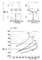
- FIGS. 3 to 6 summarize the interdependence of the well parameters (width, intra-band transition energy, position of E1, oscillator force f12 from SB1 to SB2) for various structures A, B , C and D ( Figure 3).
- FIG. 7B shows the wave functions of the first electron states of the structure for a well GaAs narrow.
- Electrons in the X valley are subjected to a potential well in the AlAs layers.
- the first type X levels of the structure have an energy close to 180 meV compared to the bottom of the well.
- the first electronic level of conduction of the structure is the first level of the family X and not the level E1 of the structure (see fig. 7B) .
- the barriers are made of AlAs and the well consists of a layer of GaAs (structure A), of In 0.2 Ga 0.8 As (structure B), of a GaAs layer with two monolayers of InAs in the middle (structure C according to the invention) or a GaAs layer with three monolayers of InAs in the middle (structure D according to the invention).
- E2-E1 is given as a function of the width a of the well, the bold lines corresponding to the range of possible use of these quantum wells.
- the oscillator strength f12 of the intra-band transition is given as a function of E2-E1, the bold lines corresponding to the range of possible use of these quantum wells.
- the maximum value reached is around 600 meV (see Figure 5, structure (A)).
- the electronic properties are then very sensitive to the quality of the structure and to the perfection of the interfaces in particular.
- This material has a lattice parameter different from GaAs but can however be deposited in a constrained thin layer on GaAs.
- the first problem (position with respect to X1) is alleviated by the overall displacement of the levels of the well.
- Transition energies of the order of 600 meV are a priori thus accessible.
- the third problem is not alleviated: in the range of accessible transition energies, the dependence of E2-E1 as a function of the width of the well is almost identical for a well of GaAs or of In 0.2 Ga 0 , 8 As (in both cases, AlAs acts as an infinite height barrier).
- GaSb has a bandgap energy of 0.75 eV at low temperature, which makes it an interesting material for optoelectronics.
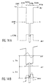
- FIG. 14A The configuration of bands for GaSb, AlSb (and InAs materials used in heterostructures according to the invention) is presented in FIG. 14A where BV and BC represent the valence band and the conduction band respectively.
- the in-band transition energy can be at most 150 to 200 meV: indeed, the minimum of the L band of AlSb is placed 80 meV above the minimum gamma of GaSb.
- the energy difference E2-E1 saturates at 0.6 eV and then decreases for a well width less than 2.8 nm.
- the well is constituted by a layer of GaAs and a layer of alloy Ga x Al 1-x As (0 ⁇ x ⁇ 1), placed between barrier layers of AlAs.
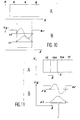
- Figure 9 shows the variations of the oscillator force f13 as a function of the energy of transition E3-E1 as well as the accessible domain II (the hatched domain I is inaccessible) using this type of well for the GaAs / AlAs system.
- FIG. 10 shows, in its part A, a known semiconductor heterostructure, of the kind of that of FIG. 1 and comprising a well layer 6 between two barrier layers 8 to form a quantum well.
- Part B of FIG. 10 shows the wave function of the states of the first two corresponding sub-bands, the minimum energies of which are denoted E1 and E2 respectively.
- Figure 11 relates to a heterostructure according to the invention.
- the invention is in fact based on a observation mentioned in document (6) that the substitution of an ultrafine layer of the quantum well material by a semiconductor material of the same family (III-V or II-VI for example) can significantly and selectively modify , the energy positions of the different sub-bands.
- the heterostructure according to the invention represented in part A of FIG. 11, comprises a well layer comprised between two barrier layers as well as an ultrathin S layer (composed of a few monolayers), attractive and inserted in the center of the well obtained.
- the barrier layers bear the reference 12 and the well layer, in which the layer S is inserted, is therefore in two parts bearing the references 10a and 10b respectively.
- a monolayer has a thickness of the order of 0.3 nm.
- Part B of FIG. 11 shows the new potential profile of the well thus obtained.
- An electron in the SB1 sub-band has a high density of probability of presence at the center of the quantum well.
- GaAs / AlAs systems i.e. Ga 1-x Al x As for the well layer and Ga 1-y Al y As for the layers -barriers, with x positive or zero and less than y and y less than or equal to 1
- GaSb / AlSb i.e. Ga 1-x Al x Sb for the well layer and Ga y Al 1- y Sb for the barrier layers, with x positive or zero and less than y and y less than or equal to 1).
- GaAs / AlAs system for example InAs (or more precisely In z Ga 1-z As with z positive and less than or equal to 1) is used to produce the layer S which disturbs the GaAs / AlAs structure.
- InAs or more precisely In z Ga 1-z As with z positive and less than or equal to 1 is used to produce the layer S which disturbs the GaAs / AlAs structure.
- InAs is a material with a smaller prohibited band than GaAs and makes it possible to generate an attractive disturbance in the latter.
- a very thin layer of InAs comprising two monolayers which are deposited on GaAs by a conventional growth technique (EJM or OMCVD).
- Intra-band absorption at energies exceeding 0.8 eV is made possible.
- the width of the well is greater in the case of the modified structure.
- the layer S For the structures used under electric field, one could prefer to place the layer S at the node of the wave function of the second level (in order to move this one as little as possible) or to the maximum of density of propability of presence of the first level (to lower it as much as possible).
- This displacement can be compensated by an offset from the nominal position of the InAs plane.
- This one has a strong attractive character for the electrons because the discontinuity of bands in the vicinity of the interface InAs / GaSb is worth 1 eV.
- FIG. 14A the configuration of bands for the InAs, GaSb and AlSb materials is shown in FIG. 14A.
- n monolayers (n greater than or equal to 2 and less than or equal to 6) of GaSb by InAs at the center of the well makes it possible to greatly increase the range of transition energies accessible in this system, as shown in FIGS. 12 and 13 in which the bold lines correspond to the range of possible use of the quantum wells.
- a is the width of a well (thickness of GaSb plus thickness of the n MC monolayers of InAs).
- An advantage of this system compared to the InAs / GaAs / AlAs system is that a desired value E2-E1 can be obtained here starting from a larger well which is therefore more easily achievable and less susceptible to imperfections.
- n for n greater than or equal to 4, is an overall displacement of the levels E1 and E2 towards low energies and a corresponding reduction in the bandgap energy of the structure.
- a second advantage of this system is therefore that the intra-band transition energy (very sensitive to the width of the well) and the band gap energy can be adjusted relatively independently if necessary.
- InSb two or three monolayers
- InSb In
- a component uses intra-band absorption, it is therefore possible to extend its operating range towards short wavelengths by modifying only, in accordance with the invention, the well (or the wells in the case of a quantum multi-well structure) where intra-band absorption occurs.
- the in-band transition energy and the energy E 1 -HH 1 of the band gap of the structure are simultaneously very close to 0.8 eV.
- the second harmonic generation coefficient is proportional to: ⁇ t ⁇ 2> ⁇ 2 z ⁇ 1> ⁇ 1 ⁇ t> (E2-Et-2hv) (E1-Et-hv)
- the interband (in the order of 0.79 eV) and inband (in the order of 0.81 eV) transition energies are simultaneously close to the resonance at 0.8 eV.
- ⁇ 2> are large (they are worth 0.63 and 0.42 respectively) and the oscillator strength of the in-band transition (linked to the matrix element ⁇ 1
- an undoped version of the structure of the invention can constitute the active medium of an all-optical modulator, working at 1.55 micrometer and controlled by radiation of the same wavelength.
Description
La présente invention concerne une hétérostructure semiconductrice qui permet une absorption intra-bande efficace d'un rayonnement électromagnétique dont la longueur d'onde est inférieure ou égale à 3 micromètres.The present invention relates to a semiconductor heterostructure which allows efficient intra-band absorption of electromagnetic radiation whose wavelength is less than or equal to 3 micrometers.
En d'autres termes, une hétérostructure conforme à la présente invention est capable d'absorber dans une fenêtre spectrale étroite qui est centrée sur une longueur d'onde donnée, inférieure ou égale à 3 micromètres.In other words, a heterostructure according to the present invention is capable of absorbing in a narrow spectral window which is centered on a given wavelength, less than or equal to 3 micrometers.
L'hétérostructure objet de l'invention peut constituer le milieu actif d'un détecteur, d'un modulateur ou d'un filtre stoppe-bande fonctionnant à des longueurs d'onde inférieures ou égales à 3 micromètres, ces longueurs d'onde étant par exemple comprises entre 1,5 micromètre et 3 micromètres.The heterostructure which is the subject of the invention can constitute the active medium of a detector, a modulator or a stop-band filter operating at wavelengths less than or equal to 3 micrometers, these wavelengths being for example between 1.5 micrometer and 3 micrometers.
L'invention a donc des applications en optoélectronique et en particulier dans le domaine des télécommunications par fibres optiques.The invention therefore has applications in optoelectronics and in particular in the field of telecommunications by optical fibers.
Elle permet d'introduire une nouvelle famille de composants qui fonctionnent au voisinage des longueurs d'onde 1,55 micromètre et 2,5 micromètres, correspondant au minima d'atténuation des fibres optiques classiques et des fibres de nouvelle génération à base de verres fluorés.It makes it possible to introduce a new family of components which operate in the vicinity of the wavelengths 1.55 micrometer and 2.5 micrometers, corresponding to the minimum attenuation of conventional optical fibers and of new generation fibers based on fluorinated glasses. .
On va d'abord rappeler le mécanisme d'absorption intra-bande dans une structure à puits quantique.We will first recall the intra-band absorption mechanism in a quantum well structure.
Ce mécanisme est exploité par une famille de composants semiconducteurs (détecteurs, modulateurs) qui travaillent essentiellement dans l'infrarouge lointain (longueurs d'onde de l'ordre de 10 micromètres).This mechanism is operated by a family of semiconductor components (detectors, modulators) which work mainly in the far infrared (wavelengths of the order of 10 micrometers).
Pour les structures semiconductrices connues, la longueur d'onde minimale de fonctionnement est de l'ordre de 3,5 micromètres.For known semiconductor structures, the minimum operating wavelength is of the order of 3.5 micrometers.
La présente invention propose une hétérostructure semiconductrice qui permet d'augmenter considérablement la plage de fonctionnement efficace des dispositifs utilisant l'absorption intra-bande.The present invention provides a semiconductor heterostructure which greatly increases the effective operating range of devices using intra-band absorption.
En faisant référence à la figure 1 partie A, on rappelle qu'un puits quantique est obtenu par l'insertion d'une couche mince 2 d'un matériau semiconducteur entre deux couches semiconductrices 4 dont la bande interdite a une largeur supérieure à celle de la couche 2, ces couches 4 étant appelées "couches-barrières".Referring to FIG. 1, part A, it is recalled that a quantum well is obtained by the insertion of a
On utilise en général des matériaux d'une même famille semiconductrice (III-V, II-VI ou IV) pour réaliser les couches 2 et 4.In general, materials from the same semiconductor family (III-V, II-VI or IV) are used to make
A cause de la modulation de la composition de l'empilement ainsi obtenu, un électron placé dans la bande de conduction BC "voit" un puits de potentiel artificiel dont le profil est rappelé sur la partie B de la figure 1.Because of the modulation of the composition of the stack thus obtained, an electron placed in the conduction band BC "sees" a well of artificial potential whose profile is recalled on part B of FIG. 1.
On note z la direction de l'espace suivant laquelle est réalisé l'empilement, et x et y des directions orthogonales dans le plan des couches de l'empilement.We denote by z the direction of the space along which the stack is made, and x and y orthogonal directions in the plane of the layers of the stack.
La mécanique quantique enseigne que les états électroniques de conduction d'une telle structure se rassemblent, à cause du confinement des électrons suivants z, en plusieurs sous-bandes qui sont quasiment parallèles.Quantum mechanics teaches that the electronic conduction states of such a structure come together, due to the confinement of the following electrons z, in several sub-bands which are almost parallel.
Les énergies des minima de ces sous-bandes prennent des valeurs discrètes.The minima energies of these sub-bands take discrete values.
Les deux premières sous-bandes sont respectivement notées SB1 et SB2 et les énergies des minima des sous-bandes SB1 et SB2 sont respectivement notées E1 et E2, avec E2 supérieur à E1.The first two sub-bands are respectively denoted SB1 and SB2 and the energies of the minima of the sub-bands SB1 and SB2 are respectively denoted E1 and E2, with E2 greater than E1.
Ceci est illustré par la figure 2 qui montre les courbes de dispersion des sous-bandes SB1 et SB2, E représentant l'énergie et k// représentant le module du vecteur d'onde d'un électron dans le plan (x, y).This is illustrated by FIG. 2 which shows the dispersion curves of the sub-bands SB1 and SB2, E representing the energy and k // representing the modulus of the wave vector of an electron in the plane (x, y) .
On voit aussi sur la partie B de la figure 1 (où V(z) représente la valeur du potentiel en fonction de z) que la densité de probabilité de présence |φ1|2 d'un électron de la sous-bande SB1 est forte au centre du puits quantique.We also see in part B of Figure 1 (where V (z) represents the value of the potential as a function of z) that the density of probability of presence | φ1 | 2 of an electron in the SB1 subband is strong at the center of the quantum well.
Au contraire, la densité de probabilité de présence |φ2|2 d'un électron de la sous-bande SB2 est nulle au centre du puits.On the contrary, the density of probability of presence | φ2 | 2 of an electron of the sub-band SB2 is zero in the center of the well.
Il est possible de peupler les niveaux de plus basse énergie du puits par des électrons, en dopant par des donneurs la couche 2 et/ou les couches-barrières 4.It is possible to populate the lower energy levels of the well with electrons, by doping with
On peut également photo-créer un gaz d'électrons, en excitant optiquement la structure avec un rayonnement d'énergie supérieure à la largeur de bande interdite de cette structure.It is also possible to photo-create an electron gas, by optically exciting the structure with radiation of energy greater than the forbidden bandwidth of this structure.
Les états de conduction sont alors peuplés jusqu'à une certaine énergie EF (niveau de Fermi), les états supérieurs restant quasiment vides.The conduction states are then populated up to a certain energy EF (Fermi level), the upper states remaining almost empty.
Ceci est illustré par la figure 2 où la référence ep désigne les états de conduction peuplés et la référence ev désigne les états de conduction vides.This is illustrated by FIG. 2 where the reference ep designates the populated conduction states and the reference ev designates the empty conduction states.
L'absorption intra-bande, encore appelée absorption inter-sous-bande, est une transition optique, d'un état d'une sous-bande vers un état d'une sous-bande supérieure, cette transition s'accompagnant de l'absorption d'un photon.Intra-band absorption, also called inter-sub-band absorption, is an optical transition from a state of a sub-band to a state of an upper sub-band, this transition being accompanied of the absorption of a photon.
Cette transition nécessite que plusieurs conditions soient satisfaites:
- k// est (quasiment) conservé,
- l'énergie h.v du photon (où h représente la constante de Planck et v la fréquence de ce photon) est égale à la différence d'énergie entre le niveau initial et le niveau final,
- le niveau de départ doit être peuplé.
- k // is (almost) preserved,
- the energy hv of the photon (where h represents the Planck constant and v the frequency of this photon) is equal to the energy difference between the initial level and the final level,
- the starting level must be populated.
Ce phénomène est illustré par la figure 2.This phenomenon is illustrated in Figure 2.
Compte tenu du quasi-parallélisme des sous-bandes , on voit que pour une structure donnée et deux de ces sous-bandes, en général SB1 et SB2, l'absorption du rayonnement électromagnétique est résonnante pour une énergie hv égale à E2-E1.Given the quasi-parallelism of the sub-bands, it can be seen that for a given structure and two of these sub-bands, in general SB1 and SB2, the absorption of electromagnetic radiation is resonant for an energy hv equal to E2-E1.
En fait, pour des structures telles que E2-E1 soit inférieure à 0,25 eV, le pic d'absorption a une largeur finie de l'ordre de 6 à 7 meV, qui reflète le court temps de vie (temps de déphasage) de l'électron dans son état d'arrivée après absorption.In fact, for structures such as E2-E1 is less than 0.25 eV, the absorption peak has a finite width of the order of 6 to 7 meV, which reflects the short life time (phase shift time) of the electron in its arrival state after absorption.
Pour des transitions à énergie plus élevée, on peut observer des effets d'élargissement qui sont dus à la non parabolicité de la bande de conduction des matériaux semiconducteurs utilisés pour réaliser le puits quantique.For higher energy transitions, broadening effects can be observed which are due to the non-parabolicity of the conduction band of the semiconductor materials used to make the quantum well.
On rappelle enfin qu'on définit la force d'oscillateur fij de la transition de la sous-bande SBi vers la sous-bande SBj par la formule suivante :![]()
![]()
Dans le cas usuel d'un puits dont la seule première sous-bande est peuplée, l'absorption totale associée à la transition de SB1 vers SBj, intégrée sur l'ensemble de la raie de résonance est proportionnelle, pour une configuration donnée d'excitation (angle d'incidence et polarisation du rayonnement électromagnétique) au produit de la force d'oscillateurs f1j par la densité de porteurs dans le puits, cette densité étant usuellement comprise entre 1011 et 1012 porteurs par cm2.In the usual case of a well whose only first sub-band is populated, the total absorption associated with the transition from SB1 to SBj, integrated over the entire resonance line is proportional, for a given configuration of excitation (angle of incidence and polarization of the electromagnetic radiation ) the product of the force of oscillators f1j by the density of carriers in the well, this density usually being between 10 11 and 10 12 carriers per cm 2 .
On réalise usuellement des multi-puits quantiques, dans lesquels la structure absorbante est répétée une cinquantaine de fois pour augmenter le coefficient d'absorption de la structure tout en conservant une épaisseur raisonnable pour celle-ci.Usually quantum multi-wells are produced, in which the absorbent structure is repeated fifty times to increase the absorption coefficient of the structure while retaining a reasonable thickness for it.
Parmi les dispositifs utilisant l'absorption intra-bandes, on connaît :
- les filtres stoppe-bande,
- les détecteurs photoconducteurs à puits quantiques (voir le document (1) qui comme les autres documents cités par la suite, est mentionné à la fin de la présente description)
- les modulateurs à commande électrique dont un exemple est donné dans le document (2)
- les modulateurs à commande optique dont un exemple est donné dans le document (3).
- band stop filters,
- photoconductive detectors with quantum wells (see document (1) which, like the other documents cited below, is mentioned at the end of this description)
- electrically controlled modulators, an example of which is given in document (2)
- optically controlled modulators, an example of which is given in document (3).
L'ensemble de ces applications connues de l'absorption intra-bande a été développé dans la plage allant de 5 à 20 micromètres.All of these known applications of intra-band absorption have been developed in the range from 5 to 20 micrometers.
La présente invention vise à étendre vers les courtes longueurs d'onde la plage de fonctionnement de ces dispositifs et, pour ce faire, d'étendre la plage d'énergie dans laquelle il est possible d'obtenir une absorption intra-bande efficace.The present invention aims to extend towards the short wavelengths the operating range of these devices and, to do this, to extend the energy range in which it is possible to obtain efficient intra-band absorption.
Le document (4) montre l'intérêt des puits quantiques pour le doublage de fréquence dans l'infrarouge moyen (5 à 20 micromètres).Document (4) shows the interest of quantum wells for frequency doubling in medium infrared (5 to 20 micrometers).
Cependant, la technique mentionnée dans ce document (4) ne peut être étendue à des énergies supérieures à 0,3 eV.However, the technique mentioned in this document (4) cannot be extended to energies greater than 0.3 eV.
Il est également connu, par le document (5), d'utiliser des puits asymétriques pour réaliser une opération de génération de seconde harmonique au voisinage de leur énergie de bande interdite mais cette génération de seconde harmonique n'est pas efficace pour de grandes énergies (par exemple 0,8 eV).It is also known, from document (5), to use asymmetric wells to carry out an operation for generating a second harmonic in the vicinity of their band gap energy, but this generation of second harmonic is not effective for large energies. (e.g. 0.8 eV).
Comme on le verra par la suite, certaines structures conformes à la présente invention permettent d'obtenir un fort coefficient de génération de seconde harmonique à partir d'un rayonnement proche-infrarouge (0,8 eV par exemple).As will be seen below, certain structures in accordance with the present invention make it possible to obtain a high coefficient of generation of second harmonic from near-infrared radiation (0.8 eV for example).
On ajoute que deux autres approches sont a priori possibles pour agrandir la plage énergétique dans laquelle il est possible d'observer une absorption intra-bande efficace.We add that two other approaches are a priori possible to enlarge the energy range in which it is possible to observe an effective intra-band absorption.
Une première approche consiste à réduire la largeur a du puits et une deuxième approche consiste à utiliser des transitions entre SB1 et SBn, avec n supérieur à 2.A first approach consists in reducing the width a of the well and a second approach consists in using transitions between SB1 and SBn, with n greater than 2.
Cependant, ces approches sur lesquelles on reviendra en détail par la suite ne permettent pas d'obtenir une absorption efficace dans la plage d'énergies supérieures à 400 meV.However, these approaches, which we will come back to in detail later, do not make it possible to obtain effective absorption in the energy range greater than 400 meV.
La présente invention vise une hétérostructure semiconductrice qui ne présente pas ces inconvénients.The present invention relates to a semiconductor heterostructure which does not have these drawbacks.
L'invention permet d'augmenter l'espacement entre les sous-bandes SB1 et SB2 d'un puits quantique, et donc l'énergie de la transition intra-bande, tout en augmentant la force d'oscillateur de cette transition.The invention makes it possible to increase the spacing between the sub-bands SB1 and SB2 of a quantum well, and therefore the energy of the intra-band transition, while increasing the oscillator strength of this transition.
On trouve dans l'article de GERARD et al., publié dans SUPERLATTICES AND MICROSTRUCTURES vol.8, n°4, 1990, p.417 à 419, une étude de la répartition de la densité des centres de recombinaison non radiative dans un puits quantique. Les échantillons sont formés sur des substrats en GaAs. Ces échantillons consistent en des structures à multipuits quantiques contenant six puits de GaAs qui sont séparés par des barrières en AlGaAS. Dans une série d'échantillons, une monocouche de InAs est insérée un endroit déterminé dans chaque période de la structure et l'on fait varier son emplacement d'un échantillon à l'autre.We find in the article by GERARD et al., Published in SUPERLATTICES AND MICROSTRUCTURES vol.8, n ° 4, 1990, p.417 to 419, a study of the distribution of the density of non-radiative recombination centers in a well quantum. The samples are formed on GaAs substrates. These samples consist of quantum multi-well structures containing six GaAs wells which are separated by AlGaAS barriers. In a series of samples, a monolayer of InAs is inserted at a determined location in each period of the structure and its location is varied from one sample to another.
La présente invention a pour objet une hétérostructure semiconductrice conformément à la revendication 1.The subject of the present invention is a semiconductor heterostructure according to
Les matériaux constitutifs de la couche mince et des couches entre lesquelles cette couche mince se trouve peuvent appartenir à la même famille de matériaux semiconducteurs.The constituent materials of the thin layer and of the layers between which this thin layer is found may belong to the same family of semiconductor materials.
Selon un premier mode de réalisation particulier de l'hétérostructure objet de l'invention, la couche mince est en Ga1-xAlxAs et les couches entre lesquelles se trouve cette couche mince sont en Ga1- yAlyAs, x étant positif ou nul et inférieur à y, y étant inférieur ou égal à 1.According to a first particular embodiment of the heterostructure which is the subject of the invention, the thin layer is made of Ga 1-x Al x As and the layers between which this thin layer is found are made of Ga 1- y Al y As, x being positive or zero and less than y, y being less than or equal to 1.
Dans ce cas, la couche ultrafine peut être en InzGa1-zAs, z étant supérieur à 0 et inférieur ou égal à 1.In this case, the ultrafine layer can be In z Ga 1-z As, z being greater than 0 and less than or equal to 1.
Selon un deuxième mode de réalisation particulier, la couche mince est en Ga1-xAlxSb et les couches entre lesquelles se trouve cette couche mince sont en GayAl1-ySb, x étant positif ou nul et inférieur à y, y étant inférieur ou égal à 1.According to a second particular embodiment, the thin layer is made of Ga 1-x Al x Sb and the layers between which this thin layer is located are made of Ga y Al 1-y Sb, x being positive or zero and less than y, y being less than or equal to 1.
Dans ce cas, la couche ultrafine peut être en InAs.In this case, the ultrafine layer may be made of InAs.
L'hétérostructure objet de l'invention peut être dopée par des donneurs, de façon à peupler par des électrons le bas de la sous-bande dont l'énergie minimale vaut E1.The heterostructure object of the invention can be doped by donors, so as to populate with electrons the bottom of the sub-band whose minimum energy is E1.
Enfin, l'hétérostructure objet de l'invention peut comprendre plusieurs exemplaires empilés dudit motif, afin de former une structure à multipuits quantiques.Finally, the heterostructure which is the subject of the invention may comprise several stacked copies of said motif, in order to form a quantum multiwell structure.
La présente invention sera mieux comprise à la lecture de la description d'exemples de réalisation donnés ci-après à titre purement indicatif et nullement limitatif, en faisant référence aux dessins annexés sur lesquels :
- la figure 1 est une représentation schématique d'un puits quantique et des fonctions d'onde φ1 et φ2 des états des deux premières sous-bandes et a déjà été décrite,
- la figure 2 représente les courbes de dispersion de ces deux premières sous-bandes et a déjà été décrite,
- la figure 3 représente schématiquement deux structures connues et deux structures conformes à l'invention en vue de comparer leurs performances,
- la figure 4 représente les variations de E1 en fonction de E2-E1 pour ces structures,
- la figure 5 montre les variations de E2-E1 en fonction de la largeur du puits pour chaque structure,
- la figure 6 représente les variations de la force d'oscillateur f12 en fonction de cette largeur du puits pour chaque structure,
- la figure 7A montre le potentiel effectif ressenti par un électron dans un multi-puits quantique GaAs/AlAs et la figure 7B représente les fonctions d'onde des premiers états d'électrons de la structure pour un puits étroit de GaAs,
- la figure 8 représente le potentiel effectif ressenti par des électrons dans un puits asymétrique GaAs/GaxAl1-xAs/AlAs,
- la figure 9 représente les variations de f13 en fonction de E3-E1 pour le puits asymétrique de la figure 8,
- la figure 10 illustre schématiquement une hétérostructure connue,
- la figure 11 illustre schématiquement une hétérostructure conforme à l'invention pour la comparer à cette hétérostructure connue,
- les figures 12 et 13 permettent de comparer les performances de sept structures dont une est connue et les six autres sont conformes à l'invention, et
- la figure 14A illustre la configuration des extrémas de bandes dans le système InAs/GaSb/AlSb tandis que la figure 14B montre une structure InAs/GaSb/AlSb sous champ électrique.
- FIG. 1 is a schematic representation of a quantum well and of the wave functions φ1 and φ2 of the states of the first two sub-bands and has already been described,
- FIG. 2 represents the dispersion curves of these first two sub-bands and has already been described,
- FIG. 3 schematically represents two known structures and two structures in accordance with the invention in order to compare their performances,
- FIG. 4 represents the variations of E1 as a function of E2-E1 for these structures,
- FIG. 5 shows the variations of E2-E1 as a function of the width of the well for each structure,
- FIG. 6 represents the variations of the oscillator force f12 as a function of this width of the well for each structure,
- FIG. 7A shows the effective potential felt by an electron in a GaAs / AlAs quantum multi-well and FIG. 7B represents the wave functions of the first electron states of the structure for a narrow GaAs well,
- FIG. 8 represents the effective potential felt by electrons in an asymmetric GaAs / Ga x Al 1-x As / AlAs well,
- FIG. 9 represents the variations of f13 as a function of E3-E1 for the asymmetric well of FIG. 8,
- FIG. 10 schematically illustrates a known heterostructure,
- FIG. 11 schematically illustrates a heterostructure in accordance with the invention in order to compare it with this known heterostructure,
- FIGS. 12 and 13 compare the performances of seven structures, one of which is known and the other six are in accordance with the invention, and
- FIG. 14A illustrates the configuration of the band extremas in the InAs / GaSb / AlSb system while FIG. 14B shows an InAs / GaSb / AlSb structure under an electric field.
Avant de décrire des modes de réalisation particuliers de l'invention, on revient sur les deux approches envisageables qui sont mentionnées plus haut.Before describing particular embodiments of the invention, we return to the two possible approaches which are mentioned above.
La première approche consiste à réduire la largeur a du puits (voir fig.1) afin d'augmenter la distance entre SB1 et SB2.The first approach consists in reducing the width a of the well (see fig. 1) in order to increase the distance between SB1 and SB2.
En effet, les énergies E1 et E2 sont inversement proportionnelles au carré de a lorsque la hauteur Vb de la barrière de potentiel (profondeur du puits) est très supérieure à l'énergie E2.Indeed, the energies E1 and E2 are inversely proportional to the square of a when the height Vb of the potential barrier (depth of the well) is much greater than the energy E2.
De plus, la force d'oscillateur f12 de la transition de SB1 vers SB2 reste constante lorsque a diminue.In addition, the oscillator strength f12 of the transition from SB1 to SB2 remains constant when a decreases.
En conséquence, le pouvoir absorbant, à dopage donné du puits, est constant lorsque cette largeur diminue.Consequently, the absorbency, with given doping of the well, is constant when this width decreases.
Pour un fonctionnement tel que E2-E1 soit supérieur à 500 meV, E2 est au moins à 750 meV du fond du puits.For an operation such that E2-E1 is greater than 500 meV, E2 is at least 750 meV from the bottom of the well.
Dans ces conditions, on peut utiliser deux systèmes, qui permettent d'avoir une discontinuité de bande de conduction Vb suffisamment élevée pour que Vb soit très supérieur à E2 c'est-à-dire dépasse E2 d'au moins 100 meV, à savoir le système GaAs (puits)/GaxAl1- xAs (barrières) et le système GaSb (puits)/AlSb (barrières).Under these conditions, two systems can be used, which make it possible to have a conduction band discontinuity Vb high enough for Vb to be much greater than E2, that is to say exceeds E2 by at least 100 meV, namely the GaAs (well) / Ga x Al 1- x As (barriers) system and the GaSb (well) / AlSb (barriers) system.
On considère d'abord le système GaAs/AlAs.We first consider the GaAs / AlAs system.
Avec ce système, trois problèmes essentiels se présentent.With this system, three essential problems arise.
Ils sont illustrés par les figures 3 à 6 qui résument l'inter-dépendance des paramètres du puits (largeur, énergie de transition intra-bande, position de E1, force d'oscillateur f12 de SB1 vers SB2) pour diverses structures A, B, C et D (figure 3).They are illustrated by FIGS. 3 to 6 which summarize the interdependence of the well parameters (width, intra-band transition energy, position of E1, oscillator force f12 from SB1 to SB2) for various structures A, B , C and D (Figure 3).
On considère les résultats obtenus pour la structure A qui se rapporte à un puits quantique GaAs/AlAs dont on fait varier la largeur.We consider the results obtained for the structure A which relates to a GaAs / AlAs quantum well whose width is varied.
On indique ci-après le premier problème qui se pose.The first problem which arises is indicated below.
Les positions respectives des extréma de bandes aux points gamma et X de la zone de Brillouin sont représentées, pour un puits de GaAs dans AlAs, sur la figure 7A où les minima X sont en pointillés et les minima gamma en traits pleins.The respective positions of the band extrema at the gamma and X points of the Brillouin zone are shown, for a well of GaAs in AlAs, in FIG. 7A where the minima X are in dotted lines and the minima gamma in solid lines.
La figure 7B montre les fonctions d'ondes des premiers états d'électrons de la structure pour un puits étroit de GaAs.FIG. 7B shows the wave functions of the first electron states of the structure for a well GaAs narrow.
Des électrons de la vallée X sont soumis à un puits de potentiel dans les couches de AlAs.Electrons in the X valley are subjected to a potential well in the AlAs layers.
Les premiers niveaux de type X de la structure ont une énergie voisine de 180 meV par rapport au fond du puits.The first type X levels of the structure have an energy close to 180 meV compared to the bottom of the well.
On observe expérimentalement que si le puits a une largeur inférieure à 3,5 nm, le premier niveau électronique de conduction de la structure est le premier niveau de la famille X et non pas le niveau E1 de la structure (voir la fig.7B).We observe experimentally that if the well has a width less than 3.5 nm, the first electronic level of conduction of the structure is the first level of the family X and not the level E1 of the structure (see fig. 7B) .
Alors, il n'est pas possible de peupler la sous-bande SB1 pour exploiter la transition de SB1 vers SB2.So, it is not possible to populate the sub-band SB1 to exploit the transition from SB1 to SB2.
Si l'on veut que E1 soit raisonnablement inférieur à X1 (X1-E1 supérieur à 30 meV), il n'est pas possible d'obtenir des énergies de transition intra-bande supérieures à 300 meV (voir la fig.4).If we want E1 to be reasonably lower than X1 (X1-E1 greater than 30 meV), it is not possible to obtain intra-band transition energies greater than 300 meV (see fig. 4).
On précise que dans les structures de la figure 3, les barrières sont en AlAs et le puits est constitué d'une couche de GaAs (structure A), de In0,2Ga0,8As (structure B), d'une couche de GaAs avec deux monocouches de InAs en son milieu (structure C conforme à l'invention) ou encore d'une couche de GaAs avec trois monocouches de InAs en son milieu (structure D conforme à l'invention).It is specified that in the structures of FIG. 3, the barriers are made of AlAs and the well consists of a layer of GaAs (structure A), of In 0.2 Ga 0.8 As (structure B), of a GaAs layer with two monolayers of InAs in the middle (structure C according to the invention) or a GaAs layer with three monolayers of InAs in the middle (structure D according to the invention).
Sur la figure 4, les variations de E1 en fonction de E2-E1 sont représentées et la droite E1=0,15 eV limite le domaine hachuré où ces structures ne peuvent être utilisées pour réaliser une opération efficace d'absorption intra-bande.In FIG. 4, the variations of E1 as a function of E2-E1 are shown and the straight line E1 = 0.15 eV limits the hatched domain where these structures cannot be used to perform an effective intra-band absorption operation.
On indique aussi que, sur la figure 5, E2-E1 est donné en fonction de la largeur a du puits, les traits gras correspondant à la plage d'utilisation possible de ces puits quantiques.It is also indicated that, in FIG. 5, E2-E1 is given as a function of the width a of the well, the bold lines corresponding to the range of possible use of these quantum wells.
Sur la figure 6, la force d'oscillateur f12 de la transition intra-bande est donnée en fonction de E2-E1, les traits gras correspondant à la plage d'utilisation possible de ces puits quantiques.In FIG. 6, the oscillator strength f12 of the intra-band transition is given as a function of E2-E1, the bold lines corresponding to the range of possible use of these quantum wells.
On expose maintenant le deuxième problème.The second problem is now exposed.
Lorsque la largeur du puits diminue, les effets de non-parabolicité de la masse effective m* deviennent importants.When the width of the well decreases, the effects of non-parabolicity of the effective mass m * become significant.
A l'énergie E2, la masse effective est beaucoup plus lourde qu'en bas de bande.At energy E2, the effective mass is much heavier than at the bottom of the band.
Ceci limite l'augmentation de E2 ; la distance E2-E1 finit par saturer et décroître, lorsque la largeur du puits diminue.This limits the increase in E2; the distance E2-E1 ends up saturating and decreasing, when the width of the well decreases.
La valeur maximale atteinte est de l'ordre de 600 meV (voir la figure 5, structure (A)).The maximum value reached is around 600 meV (see Figure 5, structure (A)).
Le troisième problème est le suivant : cette valeur maximale est atteinte pour des largeurs de puits très faibles (2,5 nm).The third problem is as follows: this maximum value is reached for very small well widths (2.5 nm).
Les propriétés électroniques sont alors très sensibles à la qualité de la structure et à la perfection des interfaces en particulier.The electronic properties are then very sensitive to the quality of the structure and to the perfection of the interfaces in particular.
Pour résoudre ces trois problèmes, on peut cheche à remplacer GaAs par un matériau semiconducteur de plus petite bande interdite, plus précisément InyGa1-yAs.To solve these three problems, we can choose to replace GaAs with a semiconductor material with a smaller band gap, more precisely In y Ga 1-y As.
Ce matériau a un paramètre de maille différent de GaAs mais peut cependant être déposé en couche mince contrainte sur GaAs.This material has a lattice parameter different from GaAs but can however be deposited in a constrained thin layer on GaAs.
La réalisation de structures de bonne qualité comportant une cinquantaine de ces puits peut être envisagée pour y au plus égal à 0,2.The realization of good quality structures comprising about fifty of these wells can be envisaged for there at most equal to 0.2.
Ce remplacement de matériau de puits conduit essentiellement à une translation d'ensemble de la structure de bande du puits vers les basses énergies.This replacement of well material essentially leads to an overall translation of the well band structure towards low energies.
Les résultats obtenus pour un puits de In0,2Ga0,8As dans AlAs sont portés sur les figures 3 à 6 (structure (B)).The results obtained for a well of In 0.2 Ga 0.8 As in AlAs are shown in Figures 3 to 6 (structure (B)).
Le premier problème (position par rapport à X1) se trouve allégé par le déplacement d'ensemble des niveaux du puits.The first problem (position with respect to X1) is alleviated by the overall displacement of the levels of the well.
Des énergies de transition de l'ordre de 600 meV sont a priori ainsi accessibles.Transition energies of the order of 600 meV are a priori thus accessible.
Ce problème mis à part, on note que l'effet de saturation sur E2-E1 (deuxième problème) est limité, E2 atteignant plus tard la plage d'énergie où l'alourdissement de la masse joue un rôle important.This problem aside, we note that the saturation effect on E2-E1 (second problem) is limited, E2 later reaching the energy range where the weight increase plays an important role.
Par contre, le troisième problème ne se trouve pas allégé : dans la plage des énergies de transition accessibles, la dépendance de E2-E1 en fonction de la largeur du puits est quasiment identique pour un puits de GaAs ou de In0,2Ga0,8As (dans les deux cas, AlAs joue le rôle d'une barrière de hauteur infinie).On the other hand, the third problem is not alleviated: in the range of accessible transition energies, the dependence of E2-E1 as a function of the width of the well is almost identical for a well of GaAs or of In 0.2 Ga 0 , 8 As (in both cases, AlAs acts as an infinite height barrier).
On considère maintenant le système GaSb/AlSb.We now consider the GaSb / AlSb system.
GaSb a une énergie de bande interdite de 0,75 eV à basse température, ce qui en fait un matériau intéressant pour l'optoélectronique.GaSb has a bandgap energy of 0.75 eV at low temperature, which makes it an interesting material for optoelectronics.
AlSb joue le rôle d'une barrière, avec Vb=1,1 eV (très voisine de ce qu'elle vaut dans GaAs/AlAs).AlSb acts as a barrier, with Vb = 1.1 eV (very close to what it is worth in GaAs / AlAs).
La configuration de bandes pour les matériaux GaSb, AlSb (et InAs utilisé dans des hétérostructures conformes à l'invention) est présentée sur la figure 14A où BV et BC représentent respectivement la bande de valence et la bande de conduction.The configuration of bands for GaSb, AlSb (and InAs materials used in heterostructures according to the invention) is presented in FIG. 14A where BV and BC represent the valence band and the conduction band respectively.
Pour des puits simples GaSb/AlSb, l'énergie de transition intrabande peut être au maximum de 150 à 200 meV : en effet, le minimum de la bande L de AlSb est placé 80 meV au dessus du minimum gamma de GaSb.For single GaSb / AlSb wells, the in-band transition energy can be at most 150 to 200 meV: indeed, the minimum of the L band of AlSb is placed 80 meV above the minimum gamma of GaSb.
On retrouve donc ici le premier problème rencontré pour GaAs/AlAs.So here we find the first problem encountered for GaAs / AlAs.
Par ailleurs, l'écart énergétique E2-E1 sature à 0,6 eV puis décroît pour une largeur de puits inférieure à 2,8 nm.Furthermore, the energy difference E2-E1 saturates at 0.6 eV and then decreases for a well width less than 2.8 nm.
On précise maintenant la seconde approche.We now specify the second approach.
Dans le cadre de la recherche de transitions intrabandes efficaces à haute énergie, on peut également chercher à utiliser des transitions entre SB1 et SBn (n>2), plus élevées en énergie que SB2.As part of the search for efficient high-energy in-band transitions, one can also seek to use transitions between SB1 and SBn (n> 2), higher in energy than SB2.
Mais la force d'oscillateur de ces transitions est beaucoup plus faible que celle de la transition fondamentale de SB1 vers SB2.But the oscillator strength of these transitions is much weaker than that of the fundamental transition from SB1 to SB2.
Ainsi, pour un puits quantique très profond (où Vb est très grand devant les énergies En considérées), la force d'oscillateur vaut :
0 si n est impair (par symétrie)
sinon![]()
0 if n is odd (by symmetry)
if not ![]()
Cette force d'oscillateur décroît donc très vite : pour la transition de SB1 vers SB4, elle n'est déjà plus que de 3% de la force d'oscillateur de la transition fondamentale.This oscillator force therefore decreases very quickly: for the transition from SB1 to SB4, it is already only 3% of the oscillator force of the fundamental transition.
L'utilisation de puits asymétriques a déjà été proposée pour permettre (en rompant la symétrie) une transition de SB1 vers SB3.The use of asymmetric wells has already been proposed to allow (by breaking the symmetry) a transition from SB1 to SB3.
Une telle structure est présentée sur la figure 8 (où l'on voit le potentiel effectif V(z) ressenti par les électrons dans le puits et les premiers états de la structure) dans le cas du système GaAs/AlAs : le puits est constitué par une couche de GaAs et une couche d'alliage GaxAl1-xAs (0<x<1), placées entre des couches-barrières de AlAs.Such a structure is presented on figure 8 (where one sees the effective potential V (z) felt by the electrons in the well and the first states of the structure) in the case of the GaAs / AlAs system: the well is constituted by a layer of GaAs and a layer of alloy Ga x Al 1-x As (0 <x <1), placed between barrier layers of AlAs.
La figure 9 montre les variations de la force d'oscillateur f13 en fonction de l'énergie de transition E3-E1 ainsi que le domaine accessible II (le domaine hachuré I est inaccessible) en utilisant ce type de puits pour le système GaAs/AlAs.Figure 9 shows the variations of the oscillator force f13 as a function of the energy of transition E3-E1 as well as the accessible domain II (the hatched domain I is inaccessible) using this type of well for the GaAs / AlAs system.
On a fait varier x et les épaisseurs des couches constituant les puits, avec l'unique contrainte E1<0,15 eV( traduisant comme précédemment la nécessité de pouvoir placer des électrons dans la sous-bande SB1).We varied x and the thicknesses of the layers constituting the wells, with the unique constraint E1 <0.15 eV (reflecting as before the need to be able to place electrons in the sub-band SB1).
On note que les forces d'oscillateur accessibles chutent fortement lorsque l'énergie de transition croît ; pour E = 0,5 eV, f13 vaut au mieux 5% de la force d'oscillateur f12 dans un puits quantique normal.It is noted that the accessible oscillator forces fall sharply when the transition energy increases; for E = 0.5 eV, f13 is at best 5% of the oscillator force f12 in a normal quantum well.
Pour un même dopage des puits et une même configuration d'opération, on devrait donc avoir 20 fois plus de puits asymétriques (opérant sur leur transition SB1 vers SB3) que de puits symétriques (opérant sur la transition SB1 vers SB2) pour une même absorption du rayonnement électromagnétique à l'énergie 0,5 eV.For the same doping of the wells and the same operating configuration, we should therefore have 20 times more asymmetrical wells (operating on their transition SB1 to SB3) than symmetrical wells (operating on the transition SB1 to SB2) for the same absorption from electromagnetic radiation to energy 0.5 eV.
Ces puits asymétriques n'apportent donc pas de solution performante au problème à résoudre (obtenir des transitions intrabandes efficaces à haute énergie).These asymmetric wells therefore do not provide an effective solution to the problem to be solved (obtaining efficient in-band transitions at high energy).
La figure 10 montre, dans sa partie A, une hétérostructure semiconductrice connue, du genre de celle de la figure 1 et comportant une couche de puits 6 entre deux couches barrières 8 pour former un puits quantique.FIG. 10 shows, in its part A, a known semiconductor heterostructure, of the kind of that of FIG. 1 and comprising a
La partie B de la figure 10 montre la fonction d'onde des états des deux premières sous-bandes correspondantes dont les énergies minimales sont respectivement notées E1 et E2.Part B of FIG. 10 shows the wave function of the states of the first two corresponding sub-bands, the minimum energies of which are denoted E1 and E2 respectively.
La figure 11 se rapporte à une hétérostructure conforme à l'invention.Figure 11 relates to a heterostructure according to the invention.
L'invention repose en fait sur une observation mentionnée dans le document (6) de ce que la substitution d'une couche ultrafine du matériau du puits quantique par un matériau semiconducteur de la même famille (III-V ou II-VI par exemple) peut modifier de manière importante, et sélective, les positions énergétiques des différentes sous-bandes.The invention is in fact based on a observation mentioned in document (6) that the substitution of an ultrafine layer of the quantum well material by a semiconductor material of the same family (III-V or II-VI for example) can significantly and selectively modify , the energy positions of the different sub-bands.
La figure 11 illustre ceci.Figure 11 illustrates this.
L'hétérostructure conforme à l'invention, représentée sur la partie A de la figure 11, comprend une couche de puits comprise entre deux couches-barrières ainsi qu'une couche S ultramince (composée de quelques monocouches), attractive et insérée au centre du puits obtenu.The heterostructure according to the invention, represented in part A of FIG. 11, comprises a well layer comprised between two barrier layers as well as an ultrathin S layer (composed of a few monolayers), attractive and inserted in the center of the well obtained.
Les couches-barrières portent la référence 12 et la couche de puits, dans laquelle est insérée la couche S, est donc en deux parties portant respectivement les références 10a et 10b.The barrier layers bear the
Les techniques de croissance actuelles (épitaxie par jets moléculaires (EJM), épitaxie en phase vapeur à partir d'organo-métalliques (OMCVD)) permettent de contrôler le dépôt de couches très minces (quelques couches moléculaires, ou monocouches.Current growth techniques (molecular beam epitaxy (MJS), vapor phase epitaxy from organo-metals (OMCVD)) make it possible to control the deposition of very thin layers (a few molecular layers, or monolayers.
Dans les composés III-V une monocouche a une épaisseur de l'ordre de 0,3 nm.In the III-V compounds, a monolayer has a thickness of the order of 0.3 nm.
On a représenté sur la partie B de la figure 11 le nouveau profil de potentiel du puits ainsi obtenu.Part B of FIG. 11 shows the new potential profile of the well thus obtained.
On voit que la position de la deuxième sous-bande n'est pas modifiée ou en tout cas très peu modifiée (l'énergie minimale de SB2, notée E'2, étant peu différente de E2) car la densité de probabilité de présence d'un électron de SB2 est nul au centre du puits et donc très faible dans la zone où le potentiel a été perturbé par l'insertion de la couche S : un électron ne perçoit pas cette perturbation.We see that the position of the second sub-band is not changed or in any case very little changed (the minimum energy of SB2, noted E'2, being little different from E2) because the probability density of presence d 'an electron of SB2 is zero in the center of the well and therefore very weak in the zone where the potential was disturbed by the insertion of the layer S: an electron does not perceive this disturbance.
Un électron de la sous-bande SB1 a, au contraire, une forte densité de probabilité de présence au centre du puits quantique.An electron in the SB1 sub-band, on the contrary, has a high density of probability of presence at the center of the quantum well.
Son énergie, notée E'1, est très inférieure à E1 du fait de l'insertion de la couche perturbatrice et attractive S.Its energy, noted E'1, is much lower than E1 due to the insertion of the disturbing and attractive layer S.
On donne maintenant des exemples de réalisation de l'invention dans le cadre des systèmes GaAs/AlAs (c'est-à-dire Ga1-xAlxAs pour la couche de puits et Ga1-yAlyAs pour les couches-barrières, avec x positif ou nul et inférieur à y et y inférieur ou égal à 1) puis GaSb/AlSb (c'est-à-dire Ga1-xAlxSb pour la couche de puits et GayAl1-ySb pour les couches-barrières, avec x positif ou nul et inférieur à y et y inférieur ou égal à 1).We now give examples of embodiment of the invention in the context of GaAs / AlAs systems (i.e. Ga 1-x Al x As for the well layer and Ga 1-y Al y As for the layers -barriers, with x positive or zero and less than y and y less than or equal to 1) then GaSb / AlSb (i.e. Ga 1-x Al x Sb for the well layer and Ga y Al 1- y Sb for the barrier layers, with x positive or zero and less than y and y less than or equal to 1).
Dans le cas du système GaAs/AlAs, on utilise par exemple InAs (ou plus exactement InzGa1-zAs avec z positif et inférieur ou égal à 1) pour réaliser la couche S qui perturbe la structure GaAs/AlAs.In the case of the GaAs / AlAs system, for example InAs (or more precisely In z Ga 1-z As with z positive and less than or equal to 1) is used to produce the layer S which disturbs the GaAs / AlAs structure.
InAs est un matériau de plus petite bande interdite que GaAs et permet de générer une perturbation attractive dans ce dernier.InAs is a material with a smaller prohibited band than GaAs and makes it possible to generate an attractive disturbance in the latter.
Pour des questions de différence de paramètre de maille cristalline, on utilise une couche très mince de InAs comportant deux monocouches que l'on dépose sur GaAs par une technique de croissance classique (EJM ou OMCVD).For questions of crystal lattice parameter difference, a very thin layer of InAs is used comprising two monolayers which are deposited on GaAs by a conventional growth technique (EJM or OMCVD).
Certaines techniques dérivées de ces techniques de croissance classique permettent de déposer trois monocouches de InAs (voir les documents (7) et (8)).Certain techniques derived from these conventional growth techniques make it possible to deposit three monolayers of InAs (see documents (7) and (8)).
On a comparé sur les figures 3 à 6 les résultats obtenus pour la structure GaAs/AlAs de référence à ceux obtenus pour des structures modifiées par l'insertion de deux monocouches MC (structure C) ou trois monocouches MC (structure D) de InAs au centre du puits.The results obtained for the reference GaAs / AlAs structure were compared in FIGS. 3 to 6 to those obtained for structures modified by the insertion of two MC monolayers (structure C) or three MC monolayers (structure D) of InAs in the center of the well.
Ces structures modifiées conformément à l'invention permettent de résoudre les trois problèmes mentionnés plus haut.These structures modified in accordance with the invention make it possible to solve the three problems mentioned above.
En ce qui concerne le premier problème, pour une énergie de transition donnée E2-E1, E1 est beaucoup plus faible pour la structure ainsi modifiée (voir la figure 4).Regarding the first problem, for a given transition energy E2-E1, E1 is much weaker for the structure thus modified (see Figure 4).
Dans toute la plage des énergies de transition, de 0 à 0,8 eV, E1 est inférieur à la limite de 0,15 eV : il est possible de peupler efficacement la sous-bande fondamentale de la structure.Throughout the range of transition energies, from 0 to 0.8 eV, E1 is less than the limit of 0.15 eV: it is possible to effectively populate the fundamental sub-band of the structure.
En ce qui concerne le deuxième problème, l'effet de saturation de l'énergie de transition, dû à la non-parabolicité de la bande de conduction, est repoussé : pour E2-E1 donnée, E2 est en effet plus faible dans la structure modifiée.Regarding the second problem, the saturation effect of the transition energy, due to the non-parabolicity of the conduction band, is pushed back: for given E2-E1, E2 is indeed weaker in the structure modified.
La plage des énergies de transition a priori accessibles s'en trouve augmentée.The range of transition energies a priori accessible is thereby increased.
Une absorption intra-bande à des énergies dépassant 0,8 eV est rendue possible.Intra-band absorption at energies exceeding 0.8 eV is made possible.
On notera que l'utilisation de trois monocouches de InAs au lieu de deux monocouches n'augmente pas tellement cette plage.Note that the use of three monolayers of InAs instead of two monolayers does not increase this range so much.
En ce qui concerne le troisième problème, pour une énergie de transition intrabande donnée, la largeur du puits est plus grande dans le cas de la structure modifiée.With regard to the third problem, for a given in-band transition energy, the width of the well is greater in the case of the modified structure.
Cette propriété peut permettre de travailler avec des puits de plus grande largeur (4 nm au lieu de 2,3 nm pour E2-E1=0,6 eV) et de meilleure qualité structurale.This property can make it possible to work with wells of greater width (4 nm instead of 2.3 nm for E2-E1 = 0.6 eV) and of better structural quality.
On notera, pour chacun de ces trois problèmes, la supériorité des structures C et D conformes à l'invention sur la structure à puits de In0,2Ga0,8As.We will note, for each of these three problems, the superiority of structures C and D according to the invention on the structure of In 0.2 Ga 0.8 As As.
On notera enfin, sur la figure 6, que les forces d'oscillateur sont supérieures, à énergie de transition intrabande donnée, pour les structures conformes à l'invention.Finally, it will be noted, in FIG. 6, that the oscillator forces are greater, at a given in-band transition energy, for the structures according to the invention.
On précise que dans certain cas, il peut être plus intéressant de placer la couche S au voisinage du centre du puits plutôt que rigoureusement au centre de ce puits.It is specified that in certain cases, it may be more advantageous to place the layer S in the vicinity of the center of the well rather than rigorously in the center of this well.
Pour les structures utilisées sous champ électrique, on pourra préférer placer la couche S au noeud de la fonction d'onde du second niveau (afin de déplacer celui-ci aussi peu que possible) ou au maximum de densité de propabilité de présence du premier niveau (pour abaisser celui-ci autant qu'il est possible).For the structures used under electric field, one could prefer to place the layer S at the node of the wave function of the second level (in order to move this one as little as possible) or to the maximum of density of propability of presence of the first level (to lower it as much as possible).
On peut également compenser certaines imperfections de structure ; dans le cas de InAs dans GaAs et pour certaines conditions de croissance, on peut observer un étalement limité de InAs sur quelques monocouches, dans la direction de croissance.We can also compensate for certain structural imperfections; in the case of InAs in GaAs and for certain growth conditions, one can observe a limited spreading of InAs on some monolayers, in the growth direction.
Cet étalement décale alors la position moyenne de l'indium par rapport au centre du puits.This spread then shifts the average position of the indium relative to the center of the well.
Ce déplacement peut être compensé par un décalage de la position nominale du plan de InAs.This displacement can be compensated by an offset from the nominal position of the InAs plane.
On considère maintenant le cas du système GaSb/AlSb.We now consider the case of the GaSb / AlSb system.
Dans ce cas, il est possible d'épitaxier facilement sur GaSb le matériau InAs.In this case, it is possible to easily epitaxialize the InAs material on GaSb.
Celui-ci a un fort caractère attractif pour les électrons car la discontinuité de bandes au voisinage de l'interface InAs/GaSb vaut 1 eV.This one has a strong attractive character for the electrons because the discontinuity of bands in the vicinity of the interface InAs / GaSb is worth 1 eV.
Pour mémoire, la configuration de bandes pour les matériaux InAs, GaSb et AlSb est représentée sur la figure 14A.As a reminder, the configuration of bands for the InAs, GaSb and AlSb materials is shown in FIG. 14A.
Une substitution de n monocouches (n supérieur ou égal à 2 et inférieur ou égal à 6) de GaSb par InAs au centre du puits permet d'augmenter très fortement la plage des énergies de transition accessibles dans ce système, comme le montrent les figures 12 et 13 sur lesquelles les traits gras correspondent à la plage d'utilisation possible des puits quantiques.A substitution of n monolayers (n greater than or equal to 2 and less than or equal to 6) of GaSb by InAs at the center of the well makes it possible to greatly increase the range of transition energies accessible in this system, as shown in FIGS. 12 and 13 in which the bold lines correspond to the range of possible use of the quantum wells.
De plus, sur la figure 13, a est la largeur d'un puits (épaisseur de GaSb plus épaisseur des n monocouches MC de InAs).In addition, in FIG. 13, a is the width of a well (thickness of GaSb plus thickness of the n MC monolayers of InAs).
Pour n supérieur ou égal à 3, cette plage s'étend bien au-delà de 0,8 eV.For n greater than or equal to 3, this range extends well beyond 0.8 eV.
Un avantage de ce système par rapport au système InAs/GaAs/AlAs (utilisation de InAs pour former la couche S) est qu'on peut obtenir ici une valeur désirée E2-E1 en partant d'un puits plus large qui est donc plus facilement réalisable et moins sensible aux imperfections.An advantage of this system compared to the InAs / GaAs / AlAs system (use of InAs to form the S layer) is that a desired value E2-E1 can be obtained here starting from a larger well which is therefore more easily achievable and less susceptible to imperfections.
On notera que pour une largeur de puits donnée, E2-E1 augmente avec n, sature pour n égal à 4 ou à 5 et diminue ensuite.Note that for a given well width, E2-E1 increases with n, saturates for n equal to 4 or 5 and then decreases.
L'effet majeur d'une augmentation de n, pour n supérieur ou égal à 4, est un déplacement d'ensemble des niveaux E1 et E2 vers les basses énergies et une réduction correspondante de l'énergie de bande interdite de la structure.The major effect of an increase of n, for n greater than or equal to 4, is an overall displacement of the levels E1 and E2 towards low energies and a corresponding reduction in the bandgap energy of the structure.
Un second avantage de ce système est donc qu'on peut ajuster relativement indépendamment si nécessaire l'énergie de transition intra-bande (très sensible à la largeur du puits) et l'énergie de bande interdite.A second advantage of this system is therefore that the intra-band transition energy (very sensitive to the width of the well) and the band gap energy can be adjusted relatively independently if necessary.
Pour la mise en oeuvre de l'invention dans le système GaSb/AlSb, on peut utiliser une couche S de InAs relativement épaisse, de l'ordre de 1,5 nm par exemple.For the implementation of the invention in the GaSb / AlSb system, it is possible to use a layer S of relatively thick InAs, of the order of 1.5 nm per example.
Comme autre matériau de substitution dans la structure, on pourrait utiliser InSb (deux ou trois monocouches) ou In(AsSb) au lieu de InAs.As another substitute material in the structure, one could use InSb (two or three monolayers) or In (AsSb) instead of InAs.
On indique ci-après quelques modes particuliers de mise en oeuvre de l'invention.Some particular modes of implementing the invention are indicated below.
L'insertion d'une couche mince au centre du puits conformément à l'invention ne change pas les conditions d'utilisation d'une telle structure utilisant l'absorption intrabande.The insertion of a thin layer in the center of the well in accordance with the invention does not change the conditions of use of such a structure using in-band absorption.
En particulier, les conditions sur la polarisation et la direction de propagation d'un faisceau lumineux incident sont inchangées.In particular, the conditions on the polarization and the direction of propagation of an incident light beam are unchanged.
Les techniques traditionnellement employées pour augmenter l'efficacité de l'absorption intra-bande par les puits (configuration de multi-réflexion, entrée du rayonnement par une face inclinée à 45° par rapport au plan des puits, insertion de la structure dans un guide d'onde, corrugation de la surface pour réaliser un réseau de diffraction) peuvent être de même employés ici.The techniques traditionally used to increase the efficiency of intra-band absorption by the wells (multi-reflection configuration, entry of the radiation by a face inclined at 45 ° to the well plane, insertion of the structure in a guide wave, surface corrugation to achieve a diffraction grating) can also be used here.
Chaque fois qu'un composant utilise l'absorption intra-bande, il est donc possible d'étendre vers les courtes longueurs d'onde sa plage de fonctionnement en modifiant uniquement, conformément à l'invention, le puits (ou les puits dans le cas d'une structure à multipuits quantiques) où se produit l'absorption intra-bande.Whenever a component uses intra-band absorption, it is therefore possible to extend its operating range towards short wavelengths by modifying only, in accordance with the invention, the well (or the wells in the case of a quantum multi-well structure) where intra-band absorption occurs.
Pour la présentation de quelques modes préférentiels de réalisation, on ne considère donc que la zone de la structure réalisant la fonction d'absorption intra-bande.For the presentation of some preferred embodiments, we therefore only consider the area of the structure performing the intra-band absorption function.
![]()
![]()

En prenant x=0,3, y=z=1, b1=b2=3nm, p1=p2=1,8 nm et n=2,5x10¹⁸ atomes/cm3, on obtient une structure absorbant à 0,5 eV (2,5 micromètres), avec une densité surfacique électronique de 1012 électrons.cm-3. Les épaisseurs c1 et c2 sont quelconques, par exemple 5 nm.
En prenant x=0,3, y=z=1, b1=b2=3 nm, p1=p2=0,8 nm, c1=c2=5 nm et n=1018 atomes/cm3, on a une absorption à environ 0,8 eV (1,55 micromètre). Les barrières de AlAs étant très fines, l'ensemble des électrons introduit par dopage est transféré dans le puits, dont la densité électronique est voisine de 1012 électrons.cm-3.Taking x = 0.3, y = z = 1, b 1 = b 2 = 3 nm, p 1 = p 2 = 0.8 nm, c 1 = c 2 = 5 nm and n = 10 18 atoms / cm 3 , we have an absorption at about 0.8 eV (1.55 micrometer). The AlAs barriers being very fine, all of the electrons introduced by doping are transferred into the well, the electronic density of which is close to 10 12 electrons.cm -3 .
En prenant b1=b2=3 nm, p1=p2=1,0 nm, c1=c2=5 nm et n=1018 atomes/cm3, l'énergie de transition intrabande et l'énergie E1-HH1 de bande interdite de la structure sont simultanément très proches de 0,8 eV.By taking b 1 = b 2 = 3 nm, p 1 = p 2 = 1.0 nm, c 1 = c 2 = 5 nm and n = 10 18 atoms / cm 3 , the in-band transition energy and the energy E 1 -HH 1 of the band gap of the structure are simultaneously very close to 0.8 eV.
On peut donc intégrer sur un substrat de GaSb des fonctions de traitement du signal à 0,8 eV (1,55 micromètres) utilisant soit l'absorption intrabande soit l'absorption bande à bande.It is therefore possible to integrate on a GaSb substrate signal processing functions at 0.8 eV (1.55 micrometers) using either in-band absorption or band-to-band absorption.
Si l'on applique un champ électrique de l'ordre de 107 V/m pour asymétriser cette structure, on obtient la configuration de bandes représentée sur la figure 14B.If an electric field of the order of 10 7 V / m is applied to asymmetrize this structure, the strip configuration shown in FIG. 14B is obtained.
Cette structure est bien adaptée à la génération de seconde harmonique à partir r d'un rayonnement de première harmonique à 1,55 micromètre (hv=0,8 eV) : on n'a qu'un seul terme résonant puique les niveaux d'électrons (ou de trous) sont bien séparés les uns des autres ; ce terme provient du processus mettant en jeu la première sous-bande de trous lourds (de fonction d'onde φt et d'énergie minimale Et) et les deux premières sous-bandes d'électrons (de fonctions d'onde φ1 et φ2 et d'énergies minimales E1 et E2).This structure is well suited to the generation of second harmonic from r of a first harmonic radiation at 1.55 micrometer (hv = 0.8 eV): there is only one resonant term since the levels of electrons (or holes) are well separated from each other; this term comes from the process involving the first sub-band of heavy holes (of wave function φt and minimum energy Et) and the first two sub-bands of electrons (of wave functions φ1 and φ2 and of minimum energies E1 and E2).
Le coefficient de génération de seconde harmonique est proportionnel à :![]()
![]()
Les énergies de transition interbande (de l'ordre de 0,79 eV) et intrabande (de l'ordre de 0,81 eV) sont simultanément proches de la résonance à 0,8 eV.The interband (in the order of 0.79 eV) and inband (in the order of 0.81 eV) transition energies are simultaneously close to the resonance at 0.8 eV.
De plus, les termes de recouvrement <φ1|φt> et <φt|φ2> sont grands (ils valent respectivement 0,63 et 0,42) et la force d'oscillateur de la transition intrabande (liée à l'élément de matrice <φ1|z|φ2>) est également grande (elle est voisine de 0,8).In addition, the recovery terms <φ1 | φt> and <φt | φ2> are large (they are worth 0.63 and 0.42 respectively) and the oscillator strength of the in-band transition (linked to the matrix element <φ1 | z | φ2>) is also large (it is close to 0.8).
On notera enfin qu'une version non dopée de la structure de l'invention peut constituer le milieu actif d'un modulateur tout optique, travaillant à 1,55 micromètre et commandé par un rayonnement de même longueur d'onde.Finally, it should be noted that an undoped version of the structure of the invention can constitute the active medium of an all-optical modulator, working at 1.55 micrometer and controlled by radiation of the same wavelength.
Les documents cités dans la présente description sont les suivants :
- (1) Levine B.F., Choi K.K., Bethea C.G. Walker J. et Malik R.J., Appl. Phys. Lett. 5 0, 1092 (1987)
- (2) Vodjani N., Vinter B., Berger V., Böckenhoff E. et Costard E., Appl. Phys. Lett. 59, 555 (1991)
- (3) Olszakier et al, Phys. Rev. Lett., 62, 2997 (1989)
- (4) Rosencher E., Bois P., Nagle J. et Delaître S., Electron. Lett. 25, 1063 (1989)
- (5) Khurghin J., Phys Rev. B, 38, 4056 (1988)
- (6) Marzin J.Y. et Gerard J.M., Phys. Rev. Lett. 62, 2172 (1989)
- (7) Gerard J.M. et Marzin J.Y., Appl. Phys. Lett 53, 568 (1988)
- (8) Lee J.H., Hsieh K.Y. et Kolbas R.M., Phys. Rev. B 41, 7678 (1990)
- (1) Levine BF, Choi KK, Bethea CG Walker J. and Malik RJ, Appl. Phys. Lett. 5 0 , 1092 (1987)
- (2) Vodjani N., Vinter B., Berger V., Böckenhoff E. and Costard E., Appl. Phys. Lett. 59 , 555 (1991)
- (3) Olszakier et al, Phys. Rev. Lett., 62 , 2997 (1989)
- (4) Rosencher E., Bois P., Nagle J. and Delaître S., Electron. Lett. 25 , 1063 (1989)
- (5) Khurghin J., Phys Rev. B, 38 , 4056 (1988)
- (6) Marzin JY and Gerard JM, Phys. Rev. Lett. 62 , 2172 (1989)
- (7) Gerard JM and Marzin JY, Appl. Phys. Lett 53 , 568 (1988)
- (8) Lee JH, Hsieh KY and Kolbas RM, Phys. Rev. B 41 , 7678 (1990)
Claims (8)
- Semiconductor heterostructure for processing an optical signal, comprising at least one pattern including a thin film (10a, 10b) of a semiconductor material and two semiconductor barrier layers (12) between which the thin film is located and which have a larger band gap than the thin film, which creates a potential well, this heterostructure furthermore comprising an attractive ultrathin film (S) which is composed of a few monolayers, which is inserted into the thin film, substantially at the centre of the latter, and which is made of a semiconductor material belonging to the same family as the material of the thin film (10a, 10b) and has a band gap smaller than that of the thin film, the heterostructure being characterized in that it includes at least two sub-bands whose minimum energy states are confined in the potential well and whose minimum energies are respectively denoted E1 and E2, with E2 greater than E1, the depth of the potential well being very much greater than E2, and the distance between the energy minima of these sub-bands being at least equal to 400 meV so as to allow the intraband absorption of radiation with corresponding energy, the sub-band whose minimum energy is equal to E1 being capable of being populated.
- Heterostructure according to Claim 1, characterized in that the materials constituting the thin film (10a, 10b) and the layers (12) between which this thin film is located belong to the same family of semiconductor materials.
- Heterostructure according to Claim 2, characterized in that the thin film (10a, 10b) is made of Ga1-xAlxAs, and in that the layers (12) between which this thin film is located are made of Ga1-yAlyAs, x being positive or zero and less than y, y being less than or equal to 1.
- Heterostructure according to Claim 3, characterized in that the ultrathin film (S) is made of InxGa1-zAs, z being greater than 0 and less than or equal to 1.
- Heterostructure according to Claim 2, characterized in that the thin film (10a, 10b) is made of Ga1-xAlxSb, and in that the layers between which this thin film is located are made of GayAl1-ySb, x being positive or zero and less than y, y being less than or equal to 1.
- Heterostructure according to Claim 5, characterized in that the ultrathin film (S) is made of InAs.
- Heterostructure according to any one of Claims 1 to 6, characterized in that it is doped with donors so as to populate with electrons the bottom of the sub-band whose minimum energy is equal to E1.
- Heterostructure, characterized in that it comprises a stack of a plurality of heterostructures according to any one of Claims 1 to 7.
Applications Claiming Priority (2)
| Application Number | Priority Date | Filing Date | Title |
|---|---|---|---|
| FR9114831A FR2684489B1 (en) | 1991-11-29 | 1991-11-29 | SEMICONDUCTOR HETEROSTRUCTURE FOR PROCESSING AN OPTICAL SIGNAL. |
| FR9114831 | 1991-11-29 |
Publications (2)
| Publication Number | Publication Date |
|---|---|
| EP0545787A1 EP0545787A1 (en) | 1993-06-09 |
| EP0545787B1 true EP0545787B1 (en) | 1997-08-20 |
Family
ID=9419523
Family Applications (1)
| Application Number | Title | Priority Date | Filing Date |
|---|---|---|---|
| EP92403193A Expired - Lifetime EP0545787B1 (en) | 1991-11-29 | 1992-11-26 | Semiconductor heterostructure for optical signal processing |
Country Status (3)
| Country | Link |
|---|---|
| EP (1) | EP0545787B1 (en) |
| DE (1) | DE69221704T2 (en) |
| FR (1) | FR2684489B1 (en) |
Families Citing this family (1)
| Publication number | Priority date | Publication date | Assignee | Title |
|---|---|---|---|---|
| FR2693594B1 (en) * | 1992-07-07 | 1994-08-26 | Thomson Csf | Electromagnetic wave detector with quantum wells. |
-
1991
- 1991-11-29 FR FR9114831A patent/FR2684489B1/en not_active Expired - Lifetime
-
1992
- 1992-11-26 EP EP92403193A patent/EP0545787B1/en not_active Expired - Lifetime
- 1992-11-26 DE DE69221704T patent/DE69221704T2/en not_active Expired - Lifetime
Also Published As
| Publication number | Publication date |
|---|---|
| DE69221704T2 (en) | 1998-01-22 |
| EP0545787A1 (en) | 1993-06-09 |
| DE69221704D1 (en) | 1997-09-25 |
| FR2684489A1 (en) | 1993-06-04 |
| FR2684489B1 (en) | 1998-08-14 |
Similar Documents
| Publication | Publication Date | Title |
|---|---|---|
| EP0575227B1 (en) | Process and apparatus for the modulation and amplification of lightrays | |
| FR2724778A1 (en) | Optical semiconductor waveguide, optically controlled switch and wavelength converter | |
| EP0432035A1 (en) | Quantum well optical device and production process | |
| EP0638831A1 (en) | Quantum well photorefractive device | |
| WO1993015525A1 (en) | Quantum well infrared detector | |
| EP0522952B1 (en) | Field effect transistor with thin barrier layers and a thin doped layer | |
| EP0306400B1 (en) | Electromagnetic wave quantum well modulator and its use as polarizer | |
| EP0436413B1 (en) | Method and device for electrooptical modulation using the low energy oblique transition in a strongly coupled superlattice | |
| EP0545787B1 (en) | Semiconductor heterostructure for optical signal processing | |
| WO2011012833A2 (en) | Electro-optical devices based on the variation in the index or absorption in the isb transitions | |
| EP0557186B1 (en) | Quantumwell photoelectric detector with enhanced detectivity | |
| EP0557141A1 (en) | Optical frequency doubling device using semi-conductor quantum structures | |
| EP0274289B1 (en) | Superlattice optical modulator | |
| EP0736791B1 (en) | Quantum well photorefractive device | |
| EP3928428A1 (en) | Progressive wave, low characteristic impedance parametric amplifier and manufacturing method thereof | |
| EP3948409B1 (en) | Ultra-fast modulator for modulating the amplitude of laser radiation | |
| EP0658792A1 (en) | Quantum well heterostructure optical processor | |
| EP0477072B1 (en) | Multilayer electro-optical light modulator | |
| EP0640866B1 (en) | All-optical bistable device of "SEED"-type | |
| EP0554178B1 (en) | Semi-conductor optical amplifier with short switching time | |
| FR2933542A1 (en) | QUANTIC CASCADES DEVICE WITH HIGH INJECTOR | |
| EP0880047A1 (en) | Optical filter comprising a multiple quantum well structure | |
| EP0658791A1 (en) | Photorefractive cell | |
| FR2716762A1 (en) | Super network optical semiconductors for electro-optical modulators |
Legal Events
| Date | Code | Title | Description |
|---|---|---|---|
| PUAI | Public reference made under article 153(3) epc to a published international application that has entered the european phase |
Free format text: ORIGINAL CODE: 0009012 |
|
| AK | Designated contracting states |
Kind code of ref document: A1 Designated state(s): DE GB |
|
| 17P | Request for examination filed |
Effective date: 19931118 |
|
| 17Q | First examination report despatched |
Effective date: 19941214 |
|
| GRAG | Despatch of communication of intention to grant |
Free format text: ORIGINAL CODE: EPIDOS AGRA |
|
| GRAH | Despatch of communication of intention to grant a patent |
Free format text: ORIGINAL CODE: EPIDOS IGRA |
|
| GRAH | Despatch of communication of intention to grant a patent |
Free format text: ORIGINAL CODE: EPIDOS IGRA |
|
| GRAA | (expected) grant |
Free format text: ORIGINAL CODE: 0009210 |
|
| AK | Designated contracting states |
Kind code of ref document: B1 Designated state(s): DE GB |
|
| REF | Corresponds to: |
Ref document number: 69221704 Country of ref document: DE Date of ref document: 19970925 |
|
| GBT | Gb: translation of ep patent filed (gb section 77(6)(a)/1977) |
Effective date: 19971024 |
|
| PLBE | No opposition filed within time limit |
Free format text: ORIGINAL CODE: 0009261 |
|
| STAA | Information on the status of an ep patent application or granted ep patent |
Free format text: STATUS: NO OPPOSITION FILED WITHIN TIME LIMIT |
|
| 26N | No opposition filed | ||
| REG | Reference to a national code |
Ref country code: GB Ref legal event code: IF02 |
|
| REG | Reference to a national code |
Ref country code: GB Ref legal event code: 732E |
|
| REG | Reference to a national code |
Ref country code: GB Ref legal event code: 732E |
|
| PGFP | Annual fee paid to national office [announced via postgrant information from national office to epo] |
Ref country code: DE Payment date: 20101124 Year of fee payment: 19 |
|
| PGFP | Annual fee paid to national office [announced via postgrant information from national office to epo] |
Ref country code: GB Payment date: 20101124 Year of fee payment: 19 |
|
| REG | Reference to a national code |
Ref country code: DE Ref legal event code: R071 Ref document number: 69221704 Country of ref document: DE |
|
| REG | Reference to a national code |
Ref country code: GB Ref legal event code: PE20 Expiry date: 20121125 |
|
| PG25 | Lapsed in a contracting state [announced via postgrant information from national office to epo] |
Ref country code: GB Free format text: LAPSE BECAUSE OF EXPIRATION OF PROTECTION Effective date: 20121125 |