EP0545777A2 - Method for manufacturing superconducting thin film formed of oxide superconductor having a portion of a reduced thickness, superconducting thin film manufactured thereby, and superconducting device utilizing the superconducting thin film - Google Patents
Method for manufacturing superconducting thin film formed of oxide superconductor having a portion of a reduced thickness, superconducting thin film manufactured thereby, and superconducting device utilizing the superconducting thin film Download PDFInfo
- Publication number
- EP0545777A2 EP0545777A2 EP92403170A EP92403170A EP0545777A2 EP 0545777 A2 EP0545777 A2 EP 0545777A2 EP 92403170 A EP92403170 A EP 92403170A EP 92403170 A EP92403170 A EP 92403170A EP 0545777 A2 EP0545777 A2 EP 0545777A2
- Authority
- EP
- European Patent Office
- Prior art keywords
- substrate
- oxide superconductor
- principal surface
- thin film
- superconducting
- Prior art date
- Legal status (The legal status is an assumption and is not a legal conclusion. Google has not performed a legal analysis and makes no representation as to the accuracy of the status listed.)
- Granted
Links
Images
Classifications
-
- H—ELECTRICITY
- H10—SEMICONDUCTOR DEVICES; ELECTRIC SOLID-STATE DEVICES NOT OTHERWISE PROVIDED FOR
- H10N—ELECTRIC SOLID-STATE DEVICES NOT OTHERWISE PROVIDED FOR
- H10N60/00—Superconducting devices
- H10N60/20—Permanent superconducting devices
- H10N60/205—Permanent superconducting devices having three or more electrodes, e.g. transistor-like structures
- H10N60/207—Field effect devices
-
- H—ELECTRICITY
- H10—SEMICONDUCTOR DEVICES; ELECTRIC SOLID-STATE DEVICES NOT OTHERWISE PROVIDED FOR
- H10N—ELECTRIC SOLID-STATE DEVICES NOT OTHERWISE PROVIDED FOR
- H10N60/00—Superconducting devices
- H10N60/01—Manufacture or treatment
- H10N60/0912—Manufacture or treatment of Josephson-effect devices
- H10N60/0941—Manufacture or treatment of Josephson-effect devices comprising high-Tc ceramic materials
Definitions
- the present invention relates to a method for manufacturing a superconducting thin film, to a superconducting thin film and a superconducting device, and more specifically to a method for manufacturing a superconducting thin film having a portion of a reduced thickness, a superconducting thin film manufactured thereby and a superconducting device which utilizes the superconducting thin film.
- Oxide superconductors which has been recently advanced in study have higher critical temperatures than those of metal superconductors, so that they are more practical.
- Y-Ba-Cu-O type oxide superconductor has a critical temperature higher than 80 K and it is announced that Bi-Sr-Ca-Cu-O type oxide superconductor and Tl-Ba-Ca-Cu-O type oxide superconductor have critical temperatures higher than 100 K.
- the superconductor thin film is usually deposited on a single crystalline substrate, for example MgO, SrTiO3 etc., by a sputtering, an MBE (molecular beam epitaxy), a CVD (chemical vapor deposition).
- the superconductor thin film grows epitaxially on this substrate.
- oxide superconductor thin film which is deposited on a substrate having a projecting portion or a step portion on its principal surface.
- This type of the oxide superconductor thin film is often utilized for a weak-link type Josephson device and an FET type superconducting device having a superconducting channel.
- the oxide superconductor has a planar upper surface so that the portion on the projecting portion of the substrate has a reduced thickness, in which a weak-link of a Josephson junction is formed or which constitutes the superconducting channel.
- oxide superconductor thin film is an oxide superconductor thin film formed on the substrate having a step portion, in which a weak-link of a Josephson junction is formed at the step portion.
- the projecting portion and the step portion of the substrate were formed by a photo-lithography process utilizing photoresist. Therefore, the principal surface of the substrate might be sometimes contaminated by the photoresist or the photoresist remover or it sometimes might react with the photoresist remover. A trace of the photoresist or the photoresist remover might remain on the substrate.
- the oxide superconductor thin film deposited on the contaminated or reacted substrate had low crystallinity so as to have a low critical current density. Therefore, it was not practical to form the oxide superconductor thin film on the processed substrate. In addition, the oxide superconductor might react with the remaining photoresist or photoresist remover, so that the properties of the oxide superconductor thin films were substantially deteriorated.
- Another object of the present invention is to provide a superconducting thin film, which overcomes the above mentioned defects of the conventional ones.
- Still another object of the present invention is to provide a superconducting device, which overcomes the above mentioned defects of the conventional ones.
- a method for manufacturing a superconducting thin film having at least one reduced thickness portion comprising the steps of ion-implanting onto a principal surface of a crystalline substrate so as to form a lattice defect at and below the principal surface of the substrate, etching the principal surface of the substrate by a wet-etching process so that a portion of the lattice defect is hardly etched so as to form a projecting portion, and forming an oxide superconductor thin film having a planar upper surface on the etched principal surface of the substrate so that a portion of the oxide superconductor thin film at the projecting portion of the substrate has a reduced thickness.
- the method in accordance with the present invention utilizes a property of a crystalline substrate that a lattice defect portion has difficulty against etching, especially against wet-etching process. Therefore, the projecting portion can be called an "artificial etch projection", In this connection, there should be no lattice defect on a principal surface of the substrate excluding a portion which will become the projecting portion.
- the substrate is heated under oxygen atmosphere at a temperature ranging from 1050 to 1500°C for 5 to 10 hours before the ion-implantation in order to eliminate lattice defects from its principal surface.
- a temperature ranging from 1050 to 1500°C for 5 to 10 hours before the ion-implantation is that the temperature is 1100 °C and the duration time is 8 hours. If the substrate is heated at a temperature lower than 1050 °C, lattice defects of the principal surface cannot be eliminated enough. If the substrate is heated up to a temperature higher than 1500 °C, the principal surface is contaminated by vapor from a reactor.
- the ions which are implanted onto the principal surface of the substrate are selected from argon ions, neon ions and oxygen ions.
- a portion of a lattice defect on the principal surface of the substrate generated by ion-implantation of the specified ions is hardly etched so that the portion projects so as to form a quadrangular pyramid shape, when the substrate is etched by a wet-etching process.
- the projecting portion artificial etch projection
- the ions are ion-implanted by a focused ion beam apparatus. It is also preferably that H3PO4 or HCI is used for the wet-etching process.
- Crystallinity of the principal surface of the substrate may be degraded during the wet-etching process. Therefore, it is preferable that the substrate is heat-treated after the wet-etching process, again.
- the conditions of the heat-treatment are the same as those of the one which is carried out before the ion-implantation.
- the oxide superconductor thin film is a c -axis orientated oxide superconductor thin film, since the c -axis orientated thin film has a large critical current density in the direction in parallel to the substrate surface.
- the abovementioned oxide superconductor is a high-T c (high critical temperature) oxide superconductor.
- This high-T c oxide superconductor has been studied by many researchers since the discovery of Bednorz and Müller in 1986, and is said to have a superconducting critical temperature of not less than 30K.
- the oxide superconductor is a high-T c copper-oxide type compound oxide superconductor including a Y-Ba-Cu-O type compound oxide superconductor, a Bi-Sr-Ca-Cu-O type compound oxide superconductor and a Tl-Ba-Ca-Cu-O type compound oxide superconductor.
- the substrate, on which the oxide superconductor layer is deposited can be formed of an insulating substrate, preferably an oxide single crystalline substrate such as MgO, SrTiO3, CdNdAlO4, YSZ (yttrium stabilized zirconia) etc.
- oxide single crystalline substrate such as MgO, SrTiO3, CdNdAlO4, YSZ (yttrium stabilized zirconia) etc.
- a superconducting thin film comprising a substrate having a principal surface and a projecting portion on the principal surface, an oxide superconductor region having a planar upper surface formed on the principal surface of which thickness of a portion at said projecting portion is reduced, and the projecting portion of the substrate being an artificial etch projection.
- the reduced thickness portion within the oxide superconductor thin film positioned on the projecting portion of the substrate can form a weak-link of a Josephson junction.
- a superconducting device comprising a substrate having a principal surface and a projecting portion on the principal surface, an oxide superconductor region having a planar upper surface formed on the principal surface of which thickness of a portion at said projecting portion is reduced, a first and a second electrodes arranged on the upper surface of the oxide superconductor region at the both sides of the reduced thickness portion, a weak-link of a Josephson junction formed at the reduced thickness portion of the oxide superconductor region, and the projecting portion of the substrate being an artificial etch projection.
- a superconducting device comprising a substrate having a principal surface and a projecting portion on the principal surface, an oxide superconductor region having a planar upper surface formed on the principal surface of which thickness of a portion at said projecting portion is reduced, a first and a second electrodes arranged on the upper surface of the oxide superconductor region at both sides of the reduced thickness portion, a third electrode arranged above the reduced thickness portion of the oxide superconductor region through an insulator layer so that superconducting current can flow between the first and second electrodes, which can be controlled by a voltage applied to the third electrode, and the projecting portion of the substrate being formed as etch projections.
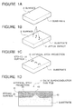
- Figures 1A to 1EE are diagrammatic views for illustrating an embodiment of the process in accordance with the present invention for manufacturing the superconducting device.
- FIG. 1A there was prepared an MgO (100) substrate 1 having a principal surface 2.
- the substrate 1 was heated up to a temperature of 1100 °C under an oxygen atmosphere for eight hours.
- argon ions were ion-implanted in a center portion of the principal surface 2 so that lined lattice defects 3 were formed.
- the condition for the argon ion-implantation was that the acceleration energy was 75KeV and the dose was 1 x 10¹⁴ to 1 x 10¹⁶ ions/cm2.
- the principal surface 2 of the substrate 1 was etched by H3PO4 so that artificial etch projections 30 of a quadrangular pyramid shape were formed on the etched principal surface 20 as shown in Figures. 1C.
- the artificial etch projections 30 were formed since the lattice defects of the crystalline surface were hardly etched by H3PO4. Almost all crystalline solids more or less have this property. If the crystallinity of the etched principal surface 20 was decreased, the heat-treatment was carried out again.
- Y1Ba2Cu3O7 & oxide superconductor thin film 4 having a thickness of 300 nanometers was deposited on the etched principal surface 20 by for example an off-axis sputtering, a reactive evaporation, an MBE, a CVD, etc, as shown in Figure 1D.
- the condition of forming the Y1Ba2Cu3O 7- ⁇ oxide superconductor thin film 4 by off-axis sputtering was as follows:
- a photoresist layer (not shown) was deposited on the oxide superconductor thin film 4 in such a manner that the deposited photoresist layer had a flat upper surface, and then, the deposited photoresist layer and the deposited oxide superconductor thin film 4 were etched back, until the upper surface of the oxide superconductor thin film 4 was planarized, as shown in Figure 1D. Then, the oxide superconductor thin film in accordance with the present invention was completed.
- the oxide superconductor thin film 4 was formed of uniform c -axis orientated Y1Ba2Cu3O 7- ⁇ oxide superconductor crystals and had a first and a second superconducting portions 41 and 42 having a rather large thickness and a third superconducting portion 43 having a reduced thickness above the artificial etch projections 30. It was possible to form a weak-link of a Josephson junction in the third superconducting portion 43 by controlling its thickness.
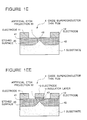
- the superconducting device was a weak-link type Josephson device.
- the superconducting device was an FET type superconducting device in which superconducting current flowing between the first and the second superconducting portions 41 and 42 through the third superconducting portion 43 was controlled by a voltage applied to the third electrode 13.
- the superconducting thin film is manufactured in accordance with the above mentioned process, an oxide superconductor thin film can be formed on a substrate having a projecting portion which is not contaminated by photoresist or photoresist remover. Therefore, the superconductivity of the oxide superconductor is not spoiled.
- the superconducting thin film is applicable to a weak-link type Josephson device and a super-FET. Accordingly, it is easy to manufacture the superconducting devices with good repeatability, and the manufactured superconducting devices have stable characteristics.
- the oxide superconductor thin film can be formed of not only the Y-Ba-Cu-O type compound oxide superconductor material, but also a high-T c (high critical temperature) oxide superconductor material, particularly a high-T c copper-oxide type compound oxide superconductor material, for example a Bi-Sr-Ca-Cu-O type compound oxide superconductor material, and a Tl-Ba-Ca-Cu-O type compound oxide superconductor material.
- a high-T c oxide superconductor material particularly a high-T c copper-oxide type compound oxide superconductor material, for example a Bi-Sr-Ca-Cu-O type compound oxide superconductor material, and a Tl-Ba-Ca-Cu-O type compound oxide superconductor material.
Abstract
Description
- The present invention relates to a method for manufacturing a superconducting thin film, to a superconducting thin film and a superconducting device, and more specifically to a method for manufacturing a superconducting thin film having a portion of a reduced thickness, a superconducting thin film manufactured thereby and a superconducting device which utilizes the superconducting thin film.
- Oxide superconductors which has been recently advanced in study have higher critical temperatures than those of metal superconductors, so that they are more practical. For example, Y-Ba-Cu-O type oxide superconductor has a critical temperature higher than 80 K and it is announced that Bi-Sr-Ca-Cu-O type oxide superconductor and Tl-Ba-Ca-Cu-O type oxide superconductor have critical temperatures higher than 100 K.
- In order to produce superconducting devices which utilize an oxide superconductor, it is necessary to form an oxide superconductor thin film. The superconductor thin film is usually deposited on a single crystalline substrate, for example MgO, SrTiO₃ etc., by a sputtering, an MBE (molecular beam epitaxy), a CVD (chemical vapor deposition). The superconductor thin film grows epitaxially on this substrate.
- In the prior art, there has been proposed an oxide superconductor thin film which is deposited on a substrate having a projecting portion or a step portion on its principal surface. This type of the oxide superconductor thin film is often utilized for a weak-link type Josephson device and an FET type superconducting device having a superconducting channel. For example, the oxide superconductor has a planar upper surface so that the portion on the projecting portion of the substrate has a reduced thickness, in which a weak-link of a Josephson junction is formed or which constitutes the superconducting channel. Another example of the oxide superconductor thin film is an oxide superconductor thin film formed on the substrate having a step portion, in which a weak-link of a Josephson junction is formed at the step portion.
- Previously, the projecting portion and the step portion of the substrate were formed by a photo-lithography process utilizing photoresist. Therefore, the principal surface of the substrate might be sometimes contaminated by the photoresist or the photoresist remover or it sometimes might react with the photoresist remover. A trace of the photoresist or the photoresist remover might remain on the substrate.
- The oxide superconductor thin film deposited on the contaminated or reacted substrate had low crystallinity so as to have a low critical current density. Therefore, it was not practical to form the oxide superconductor thin film on the processed substrate. In addition, the oxide superconductor might react with the remaining photoresist or photoresist remover, so that the properties of the oxide superconductor thin films were substantially deteriorated.
- Accordingly, it is an object of the present invention to provide a method for manufacturing a superconducting thin film, which overcomes the above mentioned defects of the conventional ones.
- Another object of the present invention is to provide a superconducting thin film, which overcomes the above mentioned defects of the conventional ones.
- Still another object of the present invention is to provide a superconducting device, which overcomes the above mentioned defects of the conventional ones.
- The above and other objects of the present invention are achieved in accordance with the present invention by a method for manufacturing a superconducting thin film having at least one reduced thickness portion, the method comprising the steps of ion-implanting onto a principal surface of a crystalline substrate so as to form a lattice defect at and below the principal surface of the substrate, etching the principal surface of the substrate by a wet-etching process so that a portion of the lattice defect is hardly etched so as to form a projecting portion, and forming an oxide superconductor thin film having a planar upper surface on the etched principal surface of the substrate so that a portion of the oxide superconductor thin film at the projecting portion of the substrate has a reduced thickness.
- In order to form a projecting portion of the substrate, the method in accordance with the present invention utilizes a property of a crystalline substrate that a lattice defect portion has difficulty against etching, especially against wet-etching process. Therefore, the projecting portion can be called an "artificial etch projection", In this connection, there should be no lattice defect on a principal surface of the substrate excluding a portion which will become the projecting portion.
- In a preferred embodiment, the substrate is heated under oxygen atmosphere at a temperature ranging from 1050 to 1500°C for 5 to 10 hours before the ion-implantation in order to eliminate lattice defects from its principal surface. One of the preferable conditions of the heat-treatment is that the temperature is 1100 °C and the duration time is 8 hours. If the substrate is heated at a temperature lower than 1050 °C, lattice defects of the principal surface cannot be eliminated enough. If the substrate is heated up to a temperature higher than 1500 °C, the principal surface is contaminated by vapor from a reactor.
- According to the present invention, it is preferable that the ions which are implanted onto the principal surface of the substrate are selected from argon ions, neon ions and oxygen ions. A portion of a lattice defect on the principal surface of the substrate generated by ion-implantation of the specified ions is hardly etched so that the portion projects so as to form a quadrangular pyramid shape, when the substrate is etched by a wet-etching process. The projecting portion (artificial etch projection) is constituted, since the crystal structure of the portion is different from the other by the lattice defect. It is possible to form the substantially same size lined projecting portions by generating lined lattice defect portions formed by the ion-implantation. Therefore, according to the present invention, it is possible to manufacture integrated superconducting device of the same properties, simultaneously.
- In a preferred embodiment, the ions are ion-implanted by a focused ion beam apparatus. It is also preferably that H₃PO₄ or HCI is used for the wet-etching process.
- Crystallinity of the principal surface of the substrate may be degraded during the wet-etching process. Therefore, it is preferable that the substrate is heat-treated after the wet-etching process, again. The conditions of the heat-treatment are the same as those of the one which is carried out before the ion-implantation.
- In a preferred embodiment, the oxide superconductor thin film is a c-axis orientated oxide superconductor thin film, since the c-axis orientated thin film has a large critical current density in the direction in parallel to the substrate surface.
- It is desired that the abovementioned oxide superconductor is a high-Tc(high critical temperature) oxide superconductor. This high-Tc oxide superconductor has been studied by many researchers since the discovery of Bednorz and Müller in 1986, and is said to have a superconducting critical temperature of not less than 30K. More specifically, the oxide superconductor is a high-Tc copper-oxide type compound oxide superconductor including a Y-Ba-Cu-O type compound oxide superconductor, a Bi-Sr-Ca-Cu-O type compound oxide superconductor and a Tl-Ba-Ca-Cu-O type compound oxide superconductor.
- In addition, the substrate, on which the oxide superconductor layer is deposited, can be formed of an insulating substrate, preferably an oxide single crystalline substrate such as MgO, SrTiO₃, CdNdAlO₄, YSZ (yttrium stabilized zirconia) etc. These substrate materials are very effective in forming or growing a crystalline film having a good superconducting property and have characteristics which are suitable for the present invention.
- According to another aspect of the present invention, there is provided a superconducting thin film comprising a substrate having a principal surface and a projecting portion on the principal surface, an oxide superconductor region having a planar upper surface formed on the principal surface of which thickness of a portion at said projecting portion is reduced, and the projecting portion of the substrate being an artificial etch projection.
- The reduced thickness portion within the oxide superconductor thin film positioned on the projecting portion of the substrate can form a weak-link of a Josephson junction.
- According to a third aspect of the present invention, there is provided a superconducting device comprising a substrate having a principal surface and a projecting portion on the principal surface, an oxide superconductor region having a planar upper surface formed on the principal surface of which thickness of a portion at said projecting portion is reduced, a first and a second electrodes arranged on the upper surface of the oxide superconductor region at the both sides of the reduced thickness portion, a weak-link of a Josephson junction formed at the reduced thickness portion of the oxide superconductor region, and the projecting portion of the substrate being an artificial etch projection.
- According to still another aspect of the present invention, there is provided a superconducting device comprising a substrate having a principal surface and a projecting portion on the principal surface, an oxide superconductor region having a planar upper surface formed on the principal surface of which thickness of a portion at said projecting portion is reduced, a first and a second electrodes arranged on the upper surface of the oxide superconductor region at both sides of the reduced thickness portion, a third electrode arranged above the reduced thickness portion of the oxide superconductor region through an insulator layer so that superconducting current can flow between the first and second electrodes, which can be controlled by a voltage applied to the third electrode, and the projecting portion of the substrate being formed as etch projections.
- The above and other objects, features and advantages of the present invention will be apparent from the following description of preferred embodiments of the invention with reference to the accompanying drawings.
- Figures 1A to 1EE are diagrammatic views for illustrating an embodiment of the process in accordance with the present invention for manufacturing the superconducting device.
- Referring to Figures 1A to 1EE, an embodiment of the process in accordance with the present invention for manufacturing the superconducting device will be described.
- As shown in Figure 1A, there was prepared an MgO (100)
substrate 1 having aprincipal surface 2. Thesubstrate 1 was heated up to a temperature of 1100 °C under an oxygen atmosphere for eight hours. - After the heat-treatment, little lattice defect was found on the
principal surface 2. If there was no lattice defect on the principal surface, the heat-treatment was not necessary. - As shown in Figure 1B, argon ions were ion-implanted in a center portion of the
principal surface 2 so that linedlattice defects 3 were formed. The condition for the argon ion-implantation was that the acceleration energy was 75KeV and the dose was 1 x 10¹⁴ to 1 x 10¹⁶ ions/cm². - Then, the
principal surface 2 of thesubstrate 1 was etched by H₃PO₄ so thatartificial etch projections 30 of a quadrangular pyramid shape were formed on the etchedprincipal surface 20 as shown in Figures. 1C.Theartificial etch projections 30 were formed since the lattice defects of the crystalline surface were hardly etched by H₃PO₄. Almost all crystalline solids more or less have this property. If the crystallinity of the etchedprincipal surface 20 was decreased, the heat-treatment was carried out again. - Thereafter, Y₁Ba₂Cu₃O₇& oxide superconductor
thin film 4 having a thickness of 300 nanometers was deposited on the etchedprincipal surface 20 by for example an off-axis sputtering, a reactive evaporation, an MBE, a CVD, etc, as shown in Figure 1D. The condition of forming the Y₁Ba₂Cu₃O7-δ oxide superconductorthin film 4 by off-axis sputtering was as follows: - Sputtering Gas
- Ar: 90%
O₂: 10% - Total pressure
- 5 x 10⁻² Torr
- Temperature of the substrate
- 700°C
- In order to planarize an upper surface of the deposited oxide superconductor
thin film 4, a photoresist layer (not shown) was deposited on the oxide superconductorthin film 4 in such a manner that the deposited photoresist layer had a flat upper surface, and then, the deposited photoresist layer and the deposited oxide superconductorthin film 4 were etched back, until the upper surface of the oxide superconductorthin film 4 was planarized, as shown in Figure 1D. Then, the oxide superconductor thin film in accordance with the present invention was completed. The oxide superconductorthin film 4 was formed of uniform c-axis orientated Y₁Ba₂Cu₃O7-δ oxide superconductor crystals and had a first and a secondsuperconducting portions third superconducting portion 43 having a reduced thickness above theartificial etch projections 30. It was possible to form a weak-link of a Josephson junction in thethird superconducting portion 43 by controlling its thickness. - Then, if there was a weak-link of a Josephson junction in the
third superconducting portion 43, a first and asecond electrodes superconducting portions - If there was not a weak-link in the
third superconducting portion 43 and a superconducting channel was formed, a first and asecond electrodes superconducting portions insulator layer 14 and a third electrode of Au were formed on thethird superconducting portion 43, as shown in Figure 1EE and the other superconducting device in accordance with the present invention was completed. In this case, the superconducting device was an FET type superconducting device in which superconducting current flowing between the first and the secondsuperconducting portions third superconducting portion 43 was controlled by a voltage applied to thethird electrode 13. - As explained above, if the superconducting thin film is manufactured in accordance with the above mentioned process, an oxide superconductor thin film can be formed on a substrate having a projecting portion which is not contaminated by photoresist or photoresist remover. Therefore, the superconductivity of the oxide superconductor is not spoiled. The superconducting thin film is applicable to a weak-link type Josephson device and a super-FET. Accordingly, it is easy to manufacture the superconducting devices with good repeatability, and the manufactured superconducting devices have stable characteristics.
- In the above mentioned embodiments, the oxide superconductor thin film can be formed of not only the Y-Ba-Cu-O type compound oxide superconductor material, but also a high-Tc (high critical temperature) oxide superconductor material, particularly a high-Tc copper-oxide type compound oxide superconductor material, for example a Bi-Sr-Ca-Cu-O type compound oxide superconductor material, and a Tl-Ba-Ca-Cu-O type compound oxide superconductor material.
- The invention has thus been shown and described with reference to the specific embodiment. However, it should be noted that the present invention is in no way limited to the details of the illustrated structures but converts and modifications may be made within the scope of the appended claims.
Claims (16)
- A method for manufacturing a superconducting thin film having at least one reduced thickness portion, the method comprising the steps of ion-implanting onto a principal surface of a crystalline substrate so as to form a lattice defect at and below the principal surface of the substrate, etching the principal surface of the substrate by a wet-etching process so that a portion of the lattice defect is hardly etched so as to form a projecting portion, and forming an oxide superconductor thin film having a planar upper surface on the etched principal surface of the substrate so that a portion of the oxide superconductor thin film at the projecting portion of the substrate has a reduced thickness.
- A method claimed in Claim 1 wherein the substrate is heated under oxygen atmosphere at a temperature ranging from 1050 to 1500°C for 5 to 10 hours before the ion-implantation in order to eliminate lattice defects from its principal surface.
- A method claimed in Claim 2 wherein the substrate is heated under oxygen atmosphere at a temperature of 1100 °C for 8 hours before the ion-implantation in order to eliminate lattice defects from its principal surface.
- A method claimed in Claim 1 wherein the substrate is heated under oxygen atmosphere at a temperature ranging from 1050 to 1500°C for 5 to 10 hours after the etching in order to improve crystallinity of its principal surface.
- A method claimed in Claim 4 wherein the substrate is heated under oxygen atmosphere at a temperature of 1100 ° C for 8 hours after the etching in order to improve crystallinity of its principal surface.
- A method claimed in Claim 1 wherein the ions which are ion-implanted are selected from argon ions, neon ions and oxygen ions.
- A method claimed in Claim 1 wherein the ions are ion-implanted by a focused ion beam apparatus.
- A method claimed in Claim 1 wherein the principal surface of the substrate is etched by H₃PO₄ or HCl.
- A method claimed in Claim 1 wherein the oxide superconductor thin film is a c-axis orientated oxide superconductor thin film.
- A method claimed in Claim 1 wherein the oxide superconductor is formed of high-Tc (high critical temperature) oxide superconductor, particularly, formed of a high-Tc copper-oxide type compound oxide superconductor.
- A method claimed in Claim 10 wherein the oxide superconductor is formed of oxide superconductor material selected from the group consisting of a Y-Ba-Cu-O type compound oxide superconductor material, a Bi-Sr-Ca-Cu-O type compound oxide superconductor material, and a Tl-Ba-Ca-Cu-O type compound oxide superconductor material.
- A method claimed in Claim 1 wherein the substrate is formed of a material selected from the group consisting of a MgO (100) substrate, a SrTiO₃ (100) substrate, a CdNdAlO₄ (001) substrate and a YSZ substrate.
- A superconducting thin film comprising a substrate having a principal surface and a projecting portion on the principal surface, an oxide superconductor region having a planar upper surface formed on the principal surface of which thickness of a portion at said projecting portion is reduced, and the projecting portion of the substrate being an artificial etch projection.
- A superconducting thin film claimed in Claim 13 wherein the reduced thickness portion of the oxide superconductor region positioned at the projecting portion of the substrate forms a weak-link of a Josephson junction.
- A superconducting device comprising a substrate having a principal surface and a projecting portion on the principal surface, an oxide superconductor region having a planar upper surface formed on the principal surface of which thickness of a portion at said projecting portion is reduced, a first and a second electrodes arranged on the upper surface of the oxide superconductor region at both sides of the reduced thickness portion, a weak-link of a Josephson junction formed at the reduced thickness portion of the oxide superconductor region, and the projecting portion of the substrate being an artificial etch projection.
- A superconducting device comprising a substrate having a principal surface and a projecting portion on the principal surface, an oxide superconductor region having a planar upper surface formed on the principal surface of which thickness of a portion at said projecting portion is reduced, a first and a second electrodes arranged on the upper surface of the oxide superconductor region at the both sides of the reduced thickness portion, a third electrode arranged above the reduced thickness portion of the oxide superconductor region through an insulator layer so that superconducting current can flow between the first and second electrodes, which can be controlled by a voltage applied to the third electrode, and the projecting portion of the substrate being an artificial etch projections.
Applications Claiming Priority (2)
| Application Number | Priority Date | Filing Date | Title |
|---|---|---|---|
| JP342466/91 | 1991-11-30 | ||
| JP3342466A JPH05148095A (en) | 1991-11-30 | 1991-11-30 | Method for making step on film-forming surface of base |
Publications (3)
| Publication Number | Publication Date |
|---|---|
| EP0545777A2 true EP0545777A2 (en) | 1993-06-09 |
| EP0545777A3 EP0545777A3 (en) | 1993-09-01 |
| EP0545777B1 EP0545777B1 (en) | 1998-09-30 |
Family
ID=18353960
Family Applications (1)
| Application Number | Title | Priority Date | Filing Date |
|---|---|---|---|
| EP92403170A Expired - Lifetime EP0545777B1 (en) | 1991-11-30 | 1992-11-25 | Method for manufacturing superconducting thin film formed of oxide superconductor having a portion of a reduced thickness, superconducting thin film manufactured thereby, and superconducting device utilizing the superconducting thin film |
Country Status (3)
| Country | Link |
|---|---|
| EP (1) | EP0545777B1 (en) |
| JP (1) | JPH05148095A (en) |
| DE (1) | DE69227172T2 (en) |
Families Citing this family (1)
| Publication number | Priority date | Publication date | Assignee | Title |
|---|---|---|---|---|
| JP2994183B2 (en) * | 1993-09-21 | 1999-12-27 | 財団法人国際超電導産業技術研究センター | Superconducting element and manufacturing method thereof |
Citations (6)
| Publication number | Priority date | Publication date | Assignee | Title |
|---|---|---|---|---|
| EP0291050A2 (en) * | 1987-05-15 | 1988-11-17 | Hitachi, Ltd. | Superconducting device |
| EP0325765A1 (en) * | 1987-12-18 | 1989-08-02 | Nec Corporation | Josephson device having a Josephson junction structure suitable for an oxide superconductor |
| WO1990000816A1 (en) * | 1988-07-06 | 1990-01-25 | Siemens Aktiengesellschaft | Josephson element with oxide ceramic superconducting material and process for manufacturing the element |
| EP0364101A2 (en) * | 1988-09-14 | 1990-04-18 | Hitachi, Ltd. | Method of forming weak-link Josephson junction, and superconducting device employing the junction |
| WO1992015406A1 (en) * | 1991-03-04 | 1992-09-17 | Superconductor Technologies, Inc. | Devices from and method for producing crystallographic boundary junctions in superconducting thin films |
| DE4109766A1 (en) * | 1991-03-25 | 1992-10-01 | Siemens Ag | Formation of Josephson weak-link junction in ceramic superconductor - by epitaxial deposition of a superconductor film on a substrate having a projecting spine on which a grain boundary is formed |
-
1991
- 1991-11-30 JP JP3342466A patent/JPH05148095A/en active Pending
-
1992
- 1992-11-25 EP EP92403170A patent/EP0545777B1/en not_active Expired - Lifetime
- 1992-11-25 DE DE69227172T patent/DE69227172T2/en not_active Expired - Fee Related
Patent Citations (6)
| Publication number | Priority date | Publication date | Assignee | Title |
|---|---|---|---|---|
| EP0291050A2 (en) * | 1987-05-15 | 1988-11-17 | Hitachi, Ltd. | Superconducting device |
| EP0325765A1 (en) * | 1987-12-18 | 1989-08-02 | Nec Corporation | Josephson device having a Josephson junction structure suitable for an oxide superconductor |
| WO1990000816A1 (en) * | 1988-07-06 | 1990-01-25 | Siemens Aktiengesellschaft | Josephson element with oxide ceramic superconducting material and process for manufacturing the element |
| EP0364101A2 (en) * | 1988-09-14 | 1990-04-18 | Hitachi, Ltd. | Method of forming weak-link Josephson junction, and superconducting device employing the junction |
| WO1992015406A1 (en) * | 1991-03-04 | 1992-09-17 | Superconductor Technologies, Inc. | Devices from and method for producing crystallographic boundary junctions in superconducting thin films |
| DE4109766A1 (en) * | 1991-03-25 | 1992-10-01 | Siemens Ag | Formation of Josephson weak-link junction in ceramic superconductor - by epitaxial deposition of a superconductor film on a substrate having a projecting spine on which a grain boundary is formed |
Non-Patent Citations (1)
| Title |
|---|
| PROCEEDINGS OF THE SPIE, vol.247, 1991, pages 205-208, New York, US; Bourne L.C. et al:"High-temperature superconducting Josephson mixers from deliberate grain boundaries in Tl2CaBa2Cu2O8" * |
Also Published As
| Publication number | Publication date |
|---|---|
| EP0545777B1 (en) | 1998-09-30 |
| DE69227172T2 (en) | 1999-05-12 |
| JPH05148095A (en) | 1993-06-15 |
| DE69227172D1 (en) | 1998-11-05 |
| EP0545777A3 (en) | 1993-09-01 |
Similar Documents
| Publication | Publication Date | Title |
|---|---|---|
| EP0533568A1 (en) | Superconducting thin film formed of oxide superconductor material, superconducting device utilizing the superconducting thin film and method for manufacturing thereof | |
| EP0366949B1 (en) | Josephson devices and process for manufacturing the same | |
| JP3064306B2 (en) | Method of forming weakly coupled Josephson junction and superconducting device using the same | |
| EP0478465B1 (en) | Method for manufacturing superconducting device having a reduced thickness of oxide superconducting layer and superconducting device manufactured thereby | |
| WO1992015406A1 (en) | Devices from and method for producing crystallographic boundary junctions in superconducting thin films | |
| EP0484253B1 (en) | Superconducting device having an extremely thin superconducting channel formed of oxide superconductor material and method for manufacturing the same | |
| EP0545816A2 (en) | Method for manufacturing a Josephson junction device having weak link of artificial grain boundary | |
| EP0325765B1 (en) | Josephson device having a josephson junction structure suitable for an oxide superconductor | |
| EP0545801A1 (en) | Superconducting device having an extremely thin superconducting channel formed of oxide superconductor material and method for manufacturing the same | |
| EP0572324A1 (en) | Josephson junction device formed of oxide superconductor and process for preparing the same | |
| EP0478464B1 (en) | Method for manufacturing a superconducting device having an extremely thin superconducting channel formed of oxide superconductor material | |
| EP0660428A2 (en) | Method for forming a step on a deposition surface of a substrate for a superconducting device utilizing an oxide superconductor | |
| EP0546904B1 (en) | Method for manufacturing an artificial grain boundary type Josephson junction device | |
| US5506197A (en) | Superconducting device having an extremely thin superconducting channel formed of oxide superconductor material | |
| EP0477103B1 (en) | Method for manufacturing superconducting device having a reduced thickness of oxide superconducting layer and superconducting device manufactured thereby | |
| EP0546958A2 (en) | Superconducting field-effect transitor having an extremly thin superconducting channel formed of oxide superconductor material | |
| EP0534811B1 (en) | Method of manufacturing superconducting thin film formed of oxide superconductor having non superconducting region in it, and method of manufacturing superconducting device utilizing the superconducting thin film | |
| EP0545777B1 (en) | Method for manufacturing superconducting thin film formed of oxide superconductor having a portion of a reduced thickness, superconducting thin film manufactured thereby, and superconducting device utilizing the superconducting thin film | |
| EP0341148B1 (en) | A semiconductor substrate having a superconducting thin film | |
| EP0488837B1 (en) | Method for manufacturing superconducting device having a reduced thickness of oxide superconducting layer and superconducting device manufactured thereby | |
| EP0358545A2 (en) | Improvement in a process for producing thallium type superconducting thin film | |
| EP0524862B1 (en) | Josephson junction device of oxide superconductor and process for preparing the same | |
| EP0546957B1 (en) | Superconducting device having an extremely thin superconducting channel formed of oxide superconductor material and method for manufacturing the same | |
| EP0533519B1 (en) | Superconducting device having an extremely thin superconducting channel formed of oxide superconductor material and method for manufacturing the same | |
| EP0545815B1 (en) | Josephson junction device formed of oxide superconductor material and process for preparing the same |
Legal Events
| Date | Code | Title | Description |
|---|---|---|---|
| PUAI | Public reference made under article 153(3) epc to a published international application that has entered the european phase |
Free format text: ORIGINAL CODE: 0009012 |
|
| AK | Designated contracting states |
Kind code of ref document: A2 Designated state(s): DE FR GB |
|
| PUAL | Search report despatched |
Free format text: ORIGINAL CODE: 0009013 |
|
| AK | Designated contracting states |
Kind code of ref document: A3 Designated state(s): DE FR GB |
|
| 17P | Request for examination filed |
Effective date: 19940218 |
|
| 17Q | First examination report despatched |
Effective date: 19950725 |
|
| GRAG | Despatch of communication of intention to grant |
Free format text: ORIGINAL CODE: EPIDOS AGRA |
|
| GRAG | Despatch of communication of intention to grant |
Free format text: ORIGINAL CODE: EPIDOS AGRA |
|
| GRAH | Despatch of communication of intention to grant a patent |
Free format text: ORIGINAL CODE: EPIDOS IGRA |
|
| GRAH | Despatch of communication of intention to grant a patent |
Free format text: ORIGINAL CODE: EPIDOS IGRA |
|
| GRAA | (expected) grant |
Free format text: ORIGINAL CODE: 0009210 |
|
| AK | Designated contracting states |
Kind code of ref document: B1 Designated state(s): DE FR GB |
|
| PG25 | Lapsed in a contracting state [announced via postgrant information from national office to epo] |
Ref country code: FR Free format text: LAPSE BECAUSE OF FAILURE TO SUBMIT A TRANSLATION OF THE DESCRIPTION OR TO PAY THE FEE WITHIN THE PRESCRIBED TIME-LIMIT Effective date: 19980930 |
|
| REF | Corresponds to: |
Ref document number: 69227172 Country of ref document: DE Date of ref document: 19981105 |
|
| PGFP | Annual fee paid to national office [announced via postgrant information from national office to epo] |
Ref country code: GB Payment date: 19981120 Year of fee payment: 7 |
|
| PGFP | Annual fee paid to national office [announced via postgrant information from national office to epo] |
Ref country code: DE Payment date: 19981126 Year of fee payment: 7 |
|
| EN | Fr: translation not filed | ||
| PLBE | No opposition filed within time limit |
Free format text: ORIGINAL CODE: 0009261 |
|
| STAA | Information on the status of an ep patent application or granted ep patent |
Free format text: STATUS: NO OPPOSITION FILED WITHIN TIME LIMIT |
|
| 26N | No opposition filed | ||
| PG25 | Lapsed in a contracting state [announced via postgrant information from national office to epo] |
Ref country code: GB Free format text: LAPSE BECAUSE OF NON-PAYMENT OF DUE FEES Effective date: 19991125 |
|
| GBPC | Gb: european patent ceased through non-payment of renewal fee |
Effective date: 19991125 |
|
| PG25 | Lapsed in a contracting state [announced via postgrant information from national office to epo] |
Ref country code: DE Free format text: LAPSE BECAUSE OF NON-PAYMENT OF DUE FEES Effective date: 20000901 |