EP0541132B1 - Image pick up apparatus having pixel compensation circuit - Google Patents
Image pick up apparatus having pixel compensation circuit Download PDFInfo
- Publication number
- EP0541132B1 EP0541132B1 EP92120395A EP92120395A EP0541132B1 EP 0541132 B1 EP0541132 B1 EP 0541132B1 EP 92120395 A EP92120395 A EP 92120395A EP 92120395 A EP92120395 A EP 92120395A EP 0541132 B1 EP0541132 B1 EP 0541132B1
- Authority
- EP
- European Patent Office
- Prior art keywords
- signal
- circuit means
- output signal
- pixel
- color
- Prior art date
- Legal status (The legal status is an assumption and is not a legal conclusion. Google has not performed a legal analysis and makes no representation as to the accuracy of the status listed.)
- Expired - Lifetime
Links
Images


Classifications
-
- H—ELECTRICITY
- H04—ELECTRIC COMMUNICATION TECHNIQUE
- H04N—PICTORIAL COMMUNICATION, e.g. TELEVISION
- H04N9/00—Details of colour television systems
- H04N9/64—Circuits for processing colour signals
- H04N9/646—Circuits for processing colour signals for image enhancement, e.g. vertical detail restoration, cross-colour elimination, contour correction, chrominance trapping filters
-
- H—ELECTRICITY
- H04—ELECTRIC COMMUNICATION TECHNIQUE
- H04N—PICTORIAL COMMUNICATION, e.g. TELEVISION
- H04N23/00—Cameras or camera modules comprising electronic image sensors; Control thereof
- H04N23/80—Camera processing pipelines; Components thereof
- H04N23/84—Camera processing pipelines; Components thereof for processing colour signals
- H04N23/88—Camera processing pipelines; Components thereof for processing colour signals for colour balance, e.g. white-balance circuits or colour temperature control
-
- H—ELECTRICITY
- H04—ELECTRIC COMMUNICATION TECHNIQUE
- H04N—PICTORIAL COMMUNICATION, e.g. TELEVISION
- H04N25/00—Circuitry of solid-state image sensors [SSIS]; Control thereof
- H04N25/10—Circuitry of solid-state image sensors [SSIS]; Control thereof for transforming different wavelengths into image signals
- H04N25/11—Arrangement of colour filter arrays [CFA]; Filter mosaics
- H04N25/13—Arrangement of colour filter arrays [CFA]; Filter mosaics characterised by the spectral characteristics of the filter elements
- H04N25/135—Arrangement of colour filter arrays [CFA]; Filter mosaics characterised by the spectral characteristics of the filter elements based on four or more different wavelength filter elements
- H04N25/136—Arrangement of colour filter arrays [CFA]; Filter mosaics characterised by the spectral characteristics of the filter elements based on four or more different wavelength filter elements using complementary colours
Definitions
- This invention relates generally to image pick up apparatus for a video camera, a facsimile, a scanner, or a copy machine, and particularly to an image pick up apparatus having a pixel compensation circuit for reducing modulation components caused by a color filter during saturation in an image pick up device thereof.
- a conventional image pick up apparatus generally comprises an image pick up device having a color filter, an amplifier for amplifying an output signal from the image pick up device, a vertical contour compensation circuit having a horizontal low-pass circuit and a horizontal contour compensation circuit for obtaining a luminance signal, a color operation circuit for obtaining color difference signals, and an encoder responsive to the luminance signal and the color difference signal for producing a color video signal. Since the luminance signal is modulated by the color filter, it is required that modulation components in the luminance signal have to be taken away.
- FIG. 22 of this specification describes a frequency interleaving system substantially as illustrated in Fig. 22 of this specification - the difference being that in Fig. 22 of the specification, the fillers W & G at the second line are in inverse order; this difference is not material.
- EP-A-0138074 relates to a color video camera signal processing circuit.
- An imager outputs white, yellow and cyan signals to separate pre-amplifiers which output to an intensity signal generating circuit and a color signal matrix circuit.
- a color temperature sensor inputs to the intensity signal generating circuit via a control signal generating circuit.
- the intensity signal generating circuit and color signal matrix circuit output through processing circuits to a color encoder.
- US-A-4131913 relates to a solid state television camera.
- the camera has a solid state image sensing device and an optical color filter.
- Horizontal scanning devices are used to produce color difference signals which, combined with a luminance signal input to an encoder.
- the present invention has been developed in order to remove the above-described drawbacks inherent to the conventional image pick up apparatus.
- an object of the present invention to provide a new and useful image pick up apparatus in which modulation components by a color filter can be reduced.
- an image pick up apparatus comprising:
- the conventional image pick up apparatus generally comprises an image pick up device 1', an amplifier 2', a 1-H delay circuit 3', a first horizontal low-pass circuit 4', a second horizontal low-pass circuit 7', a gamma correction circuit 8', a horizontal contour compensation circuit 9', an NTSC encoder 10', and a color operation circuit 200'.
- the color operation circuit 200' includes a color separation circuit 5' and a color signal processing circuit 6'.
- the color filter is provided in the image pick up device 1' for obtaining color signals of R, G, and B, and the following formulas 1 and 2 are operated in the image pick up device 1', for example.
- an arrow shows a first field I, and a dotted arrow shows a second field II.
- An output signal from the image pick up device 1' is amplified in the amplifier 2' and this amplified signal is delayed in the 1-H delay circuit 3' for providing the coincidence of an amplified signal outputted from the amplifier 2' and a delayed signal outputted from the 1-H delay circuit 3'.
- Color difference signals of (R-Y)' and (B-Y)' are obtained by means of the color operation circuit 200' with such two coincided signals of the amplified signal and the delayed signal being fed thereto.
- the coincided signals are received by the color separation circuit 5' for obtaining signals of R', G', and B', and these signals R', G', and B' are subsequently inputted into the color signal processing circuit 6' for producing color difference signals (R-Y)' and (B-Y)'.
- a luminance signal Y' is obtained by the following way. Firstly, the coincided two signals are added in an adder and the amplified signal in the coincided signals is subtracted from the delayed signal in the coincided signals. Second, an added signal outputted from the adder is fed to a first horizontal low-pass circuit 4' for cutting a high-frequency band, i.e. modulation components, and a subtracted signal from the subtractor is fed to a second horizontal low-pass circuit 7'. Since the combination of the subtractor and the second horizontal low-pass circuit 7' is vertical contour compensation circuit, an output signal from the second horizontal low-pass circuit 7' shows a vertical contour compensation signal.
- the vertical contour compensation signal and an output signal from the first horizontal circuit 4' are added, and this added signal is fed to the gamma correction circuit 8'.
- a gamma-compensated signal from the gamma compensation circuit 8' is sent to the horizontal contour compensation circuit 9' thereby producing a luminance signal Y'.
- a video signal is produced by receiving and encoding the luminance signal Y' and the color difference signals (R-Y)' and (B-Y)'.
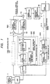
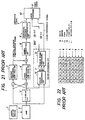
- Fig. 1 shows an image pick up device apparatus according to a first embodiment of the invention.
- the image pick up apparatus generally comprises an image pick up device 1 for picking up an image and for producing a pixel signal by using a color filter which is shown in Fig.
- the pixel compensation circuit 100 includes a pixel weighting circuit 11 and a band separating operation circuit 300 having a horizontal high-pass circuit 13, a third horizontal low-pass circuit 12, and a third adder 50.
- the structure of the first embodiment has the same structure as the prior art except for the first and second pixel compensation circuit 100 and 100'.
- the pixel signal produced by the image -pick up apparatus 1 is amplified in the amplifier 2 responsive to the pixel signal for producing an amplified pixel signal.
- the amplified pixel signal is delayed by 1-H in the 1-H delay circuit 3 for coincidentally processing the amplified signal.
- Such a delayed signal produced by 1-H delay circuit 3 is fed to the pixel compensation circuit 100, and the amplified signal is fed to the second pixel compensation circuit 100' for respectively producing a first weighted signal and a second weighted signal. Since the first and second pixel compensation circuits have the same structure, the description of the second pixel compensation circuit is omitted.
- the delayed signal is weighted in the weighting circuit 11.
- a delayed signal is weighted by a weighting signal such that modulation components caused by the difference between pixel signal levels of white and green are cancelled.
- a weighted signal is produced by multiplying the delayed signal and the weighting signal.
- Fig. 2B is a block diagram showing the pixel weighting circuit 11.
- the pixel weighting circuit 11 generally comprises a switching pulse generator 30 for generating switching pulses, a memory 28, a selector 29, and a multiplier 27. In the memory 28, factors of white and green are predetermined and stored therein, and are sent to selector 29.
- the weighting signal is defined by the factors, and is fed to the multiplier 27 from the selector 29.
- the selector 29 one of the factors is selected out in accordance with the switching pulses such that each white portion in the delayed signal corresponds to each white portion in the weighting signal as shown in Fig. 2A.
- the memory 28 outputs at least two factors which are to be multiplied by the delayed signal.
- the multiplier 27 the delayed signal is multiplied by the weighting signal thereby obtaining the weighted signal.
- selector 29 is designed as of the four-input and one-output type, and predetermined four factors are stored in the memory 28.
- Such a weighted pixel signal is fed to the horizontal high-pass circuit 13 for extracting only high-frequency components, and a delayed signal indicative of a non-weighted pixel signal is fed to the third horizontal low-pass circuit 12 for extracting only low-frequency components. Therefore, a signal in which only high-frequency components thereof are weighted is obtained by means of the third adder 50 for adding the weighted signal and the non-weighted signal. It means that modulation components caused by the color filter can be reduced and that the difference between W-G line level and CyYe level does not generate.
- a delayed signal is inputted for producing a first weighted signal.
- a non-delayed signal indicative of the output signal from the amplifier 2 is inputted for producing a second weighted signal.
- the first and second weighted signals are added, and such an added signal is sent to the first horizontal low-pass circuit 4 for cutting high-frequency components.
- the second weighted signal is sent to the vertical contour compensation circuit 500 for producing a vertical contour compensation signal to emphasize contours defined by the first and second signals. More specifically, the second weighted signal is fed to the subtractor 51 for subtracting the second weighted signal from the first weighted signal, and such a subtracted signal is supplied to the second horizontal low-pass circuit 7.
- the output signal of the second horizontal low-pass circuit 7 is a vertical contour compensation signal.
- the vertical contour compensation signal and an output signal from the first horizontal low-pass circuit 7 are added, and such an added signal is fed to the gamma correction circuit 8. Then, an output signal from the gamma correction circuit 8 is sent to the horizontal contour compensation circuit for obtaining a luminance signal.
- the color difference signals of R-Y and B-Y are obtained by means of the color operation circuit 200 responsive to a non-delayed signal and a delayed signal.
- the color separation circuit 5 is receiving the non-delayed signal and the delayed signal for producing color signals R, G, and B.
- the color signal processing circuit 6 the produced color signals R, G, and B is inputted for producing color difference signals R-Y and B-Y.
- the NTSC encode 10 produces a video signal by means of receiving the luminance Y signal and the color difference signal R-Y, B-Y.
- Fig. 3 is a block diagram of an image pick up apparatus according to a second embodiment of the invention.
- the second embodiment has a same structure as the first embodiment of Fig. 1 except for a pixel compensation circuit 101 and a pixel compensation circuit 101' having the same structure and operation as the pixel compensation circuit 101.
- a band separating operation circuit 301 is provided in the pixel compensation circuit 101. Therefore, the description of another band separating operation circuit in the pixel compensation circuit 101' is omitted.
- the band separating operation circuit 301 generally comprises a subtractor 55 for subtracting the output signal of the pixel weighting circuit 11 from the output signal of the non-weighted signal, a third horizontal low-pass circuit 12a responsive to an output signal from the subtractor 55, and an adder 54 for adding the output signal from the pixel weighting circuit 11 and an output signal from the third horizontal low-pass circuit 12a.
- Fig. 4 is an image pick up apparatus according to the third embodiment of the invention.
- image pick up devices 14 and 15 are provided.
- the image pick up device 14 has a green color filter shown in Fig. 5A
- the image pick up device 15 has a red and blue color filter shown in Fig. 5B.
- a pixel compensation circuit 102 is also provided for cutting the modulation components thereof.
- the pixel compensation circuit 102 has the same structure and operations as the pixel compensation circuits 100 or 101 described above. Then an output signal from the pixel compensation circuit 102 and a pixel signal passing through an amplifier 2a are added in an adder 56.
- the luminance signal Y the following processings are the same as the first embodiment.
- color difference signals R-Y and B-Y in a red and blue separating circuit 16 responsive to a pixel signal passing through an amplifier 2b, color signals of red and blue are outputted to a color signal processing circuit 6a.
- the output signal from the amplifier 2a and the output signals from red and blue separating circuit 16 are received and operated for producing color difference signal R-Y and B-Y.
- Fig. 6 is a block diagram showing an image pick up apparatus according to a fourth embodiment of the present invention.
- the image pick up apparatus of the invention since there are a variety of the pixel output signal level of cyan and yellow in accordance with the color temperature of images, if weighting factors are determined in accordance with the color temperatures, the modulation components caused by a color filter can be effectively reduced. On the contrary, since the pixel output signal of white and green slightly changes in accordance with the colour temperatures of images, it is not required that the weighting factors are determined by the color temperatures.
- the fourth embodiment has the same structure as the first or second embodiment of the invention except that there is provided not only the image pick up device 1 and the amplifier 2 but also a color temperature detecting circuit 17, a color temperature-clip level converter 18, and a clipper 19 as an image pick up device means.
- the color temperature detecting circuit 17 detects color temperature values of the image, and the color temperature values are fed to the color temperature-clip level converter 18 for converting each of the color temperature values into a corresponding clip level.
- Fig. 7 is a graph showing incident achromatic light-pixel signal level characteristics of an image pick up device 1 according to the fourth embodiment. As shown in Fig. 7, if the incident achromatic light is increased, a white pixel signal, a yellow pixel signal, a cyan pixel signal, and a green pixel signal are subsequently saturated. It is assumed that an input level in which the white pixel signal is saturated is Lw; an area in which any pixel signal is not saturated is area A; an area in which all pixel signals are saturated is area C; and a remaining area is area B. The pixel signal passed through the amplifier 2 is fed to the clipper 19. Fig.
- FIG. 8 is a graph showing input-output characteristics of a clipper 19 when picking up achromatic light according to the fourth embodiment.
- the saturation level Lw of the white pixel signal is a reference level
- a clip level of each of yellow, cyan, and green pixel signal is respectively defined as CYe, CCy, and CG by the saturation level Lw. Therefore, a clip level CW of the white pixel signal is necessarily defined as a saturation level in the image pick up device 1.
- Fig. 9 is a graph showing input-output characteristics of pixel compensation circuits 103 and 103' when picking up achromatic light and when the clipper 19 is not used according to the fourth embodiment. Particularly, in Fig. 9, the characteristics of high-frequency components in each pixel signal is illustrated, and the same of low-frequency components therein is shown in Fig. 7. In Fig. 9, the pixel signal level is in the areas B or C, the difference of levels between the white pixel signal and the green pixel signal is generated due to the compensation thereof. As a result, an image quality is deteriorated. If the characteristics of the clipper 19 are designed as shown in Fig. 8, the input-output characteristics of the pixel compensation circuits 103 and 103' is obtained as shown in Fig. 10.
- Fig. 10 is a graph showing input-output characteristics of pixel compensation circuits 103 and 103' when picking up achromatic light and when the clipper 19 is not used according to the fourth embodiment. Therefore, the difference of the level between the white pixel signal and the green signal level is not generated and the difference of the level between the cyan pixel signal and yellow signal is also not generated. As a result, the deterioration of an image quality is prevented.
- Fig. 11 is a block diagram of an image pick up apparatus according to a fifth embodiment of the present invention.
- the image pick up apparatus of the fifth embodiment has the same structure and operations as the fourth embodiment except that -the pixel compensation circuits 103 and 103' is not provided in the fifth embodiment. Even in the fifth embodiment, the advantageous effects caused by the clipper 19 is obtained.
- Fig. 12 is a block diagram of an image pick up apparatus according to a sixth embodiment of the present invention
- Fig. 13 is a diagram showing a structure of a color filter used in an image pick up device 1a of Fig. 12. In the sixth embodiment, two vertically adjacent pixels of on the filter is added an outputted as one pixel in each line of the fields as shown in Fig. 13.
- a pixel compensation circuit 104 has the same structure as the pixel compensation circuit 100 or 101, and a color signal generating circuit 400 responsive to the output signal from the clipper 19 for producing color difference signal is provided.
- the color signal generating circuit 400 generally comprises a horizontal high-pass circuit 20 responsive to the output signal from the clipper 19 for extracting a frequency band corresponding to a half of the sampling frequency, a detector 27 for detecting an output signal from the horizontal high-pass circuit 20, a horizontal low-pass circuit 21 responsive to an output signal from the detector 27, a white level adjusting circuit 22 for adjusting a white pixel level in output signal from the horizontal low-pass circuit 21, a 1-H delay circuit 3d responsive to an output signal from the white level adjusting circuit 22, a switching circuit 23 responsive to said output signal from the white level adjusting circuit 22 and an output signal from the 1-H delay circuit 3d for coincidentally outputting signals indicative of the color difference signals R-Y and B-Y.
- Fig. 14 is a graph showing incident achromatic light-pixel signal level characteristics of an image pick up device 1a according to the sixth embodiment.
- the difference of the level between Ye+Mg pixel signal and Cy+G pixel signal in the output signal of the pixel compensation circuit 104 is increased. Therefore, if the pixel signal level is limited as shown by the dotted lines of Fig. 14, modulation components caused by the color filter during saturation in the image pick up device 1a can be reduced.
- the clip levels are determined in accordance with the color temperature of an image, the clip levels may be stable. In this case, color signals are changed to white signal at the portion near each of corresponding clip level.
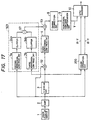
- Fig. 15 is a block diagram of an image pick up apparatus according to a seventh embodiment of the present invention.
- the image pick up apparatus has the same structure as the first embodiment except that a vertical contour compensation circuit 501 is provided instead of the vertical contour compensation circuit 500.
- the vertical contour compensation circuit 501 generally comprises a horizontal low-pass circuit 7a responsive to the second weighted signal from the pixel compensation circuit 100', a clipper 24a for clipping an output signal from the horizontal low-pass circuit 7a in accordance with a pre-determined clip value, a horizontal low-pass circuit 7b responsive to the first weighted signal outputted from the pixel compensation circuit 100, a clipper 7b for clipping an output signal from the horizontal low-pass circuit 7b in accordance with the pre-determined clip value, a subtractor 57 for subtracting an output signal of the clipper 24a from an output signal of the second clipper 24b and for sending such a subtracted signal to the adder 53.
- Fig. 16 is a graph showing input-output characteristics of high-frequency components in pixel compensation circuits 100 and 100' when picking up achromatic light and when the clipper is not used according to the seventh embodiment.
- the characteristics of low-frequency components in each output signal from the pixel compensation circuit 100 and 100' is illustrated at Fig. 7. If the incident achromatic light level is in the area B or C, the difference of level between the white pixel signal and the green pixel signal is generated as shown in Fig. 16.
- the clip levels are determined as a level of CW or below, even in the area B and C, the difference of level between an average value defined by the white and green pixel and an average value defined by the cyan and yellow pixel is not generated. As a result, the image quality is not deteriorated.
- Fig. 17 is a block diagram of an image pick up apparatus according to an eighth embodiment of the present invention.
- the image pick up apparatus of the eighth embodiment has the same structure and operations as the seventh embodiment except that the pixel compensation circuits 100 and 100' is not provided in the eighth embodiment. Even in the eighth embodiment, the above-mentioned advantageous effects caused by the vertical contour compensation circuit 501 can be achieved.
- Fig. 18 is a graph showing an output signal from the clipper 24a responding to an input signal into the second horizontal low-pass circuit 7a in the vertical contour compensation circuit 501. In this embodiment, pixel signals which are inputted into the second and third horizontal low-pass circuit 7a and 7b are shown by dotted lines of Fig.
- a WG line denotes an average value of white and green pixels
- a CyYe line denotes an average value of cyan and yellow pixels.
- clip levels of the clippers 24a and 24b are determined at the clip level CW or below whereby the difference of luminance between scanning lines forming an image is altered.
- the clip value is lower than the clip level CW due to the error of response in each of the combination circuits.
- the vertical contour compensation circuit 501 can be applied the vertical contour compensation circuit 500 through this specification.
- Fig. 19A is a block diagram showing a structure for making an n line coincident with an n+1 line by means of one 1-H delay circuit
- Fig. 19B is a block diagram showing a structure for making an n line coincident with an n+1 line by means of two 1-H delay circuits.
- a structure in which two 1-H delay circuits are used can be applied to the present embodiments.
- Fig. 20 is a block diagram showing a pixel compensation circuit having two line selectors 25 and 26 according to the ninth embodiment of the invention.
- the structure of the ninth embodiment is as follows. The output signal from the amplifier 2 is inputted into a terminal 71 of the selector 25, and the output signal from the 1-H delay circuit 3 is inputted into a terminal 72 of the selector 25.
- One output signal from the selector 25 is directly inputted into the selector 26, and the other output signal from the selector 25 is inputted, via the pixel compensation circuit 100, into the selector 26.
- An input signal of the subtractor 51 is fed from an output terminal 73 the second selector 26, and an input signal of the adder 52 is fed from the output terminal 74 of the second selector 26. More specifically, in the selector 25 responsive to the output signal from the amplifier 2 and an output signal from the 1-H delay circuit 3, one signal which is to be compensated is selected. The one signal which is to be compensated is fed to the pixel compensation circuit 100, and the other signal is directly fed to the selector 26.
- the selector 25 having the input terminal 71 in which the output signal from the amplifier 2 is inputted and the input terminal 72 in which the output signal from the 1-H delay circuit 3. Meanwhile, in the selector 26 responsive to the weighted signal and the other signal from the selector 25, such an inputted weighted signal and the other inputted signal from the selector 25 is outputted.
- the weighted signal is outputted from the terminal 73 of the selector 26 when the one signal which is to be compensated is inputted into the terminal 71 of the first selector 25 and that the weighted signal is outputted from the terminal 74 of the selector 26 when the one signal which is to be compensated is inputted into the terminal 72 of the selector 25.
- the vertical contour compensation circuit 501 and clipper 19 can be applied.
- the present embodiments are not limited by the NTSC encoder 10, and can be applied to facsimile, scanners, copy machines, etc.
Description
- This invention relates generally to image pick up apparatus for a video camera, a facsimile, a scanner, or a copy machine, and particularly to an image pick up apparatus having a pixel compensation circuit for reducing modulation components caused by a color filter during saturation in an image pick up device thereof.
- A conventional image pick up apparatus generally comprises an image pick up device having a color filter, an amplifier for amplifying an output signal from the image pick up device, a vertical contour compensation circuit having a horizontal low-pass circuit and a horizontal contour compensation circuit for obtaining a luminance signal, a color operation circuit for obtaining color difference signals, and an encoder responsive to the luminance signal and the color difference signal for producing a color video signal. Since the luminance signal is modulated by the color filter, it is required that modulation components in the luminance signal have to be taken away. However, in the conventional method using only the horizontal low-pass circuit for cutting such modulation components, when an inputted image signal level changes, such modulation components are not satisfactorily cut away thereby causing disadvantage that zigging portions in an image are generated at horizontal edge portions in low-frequency components and that jitters are generated in high-frequency components. As a result, an image quality is deteriorated.
- A conventional image pick-up apparatus is disclosed at page 90 of the Japanese publication "CCD Camera Technique" by TAKEMURA and published by radio gijutusha in 1986. Figs 5-17(a) of the document describes a frequency interleaving system substantially as illustrated in Fig. 22 of this specification - the difference being that in Fig. 22 of the specification, the fillers W & G at the second line are in inverse order; this difference is not material.
- Another prior art technique is disclosed in US-A-4205336.
- EP-A-0138074 relates to a color video camera signal processing circuit. An imager outputs white, yellow and cyan signals to separate pre-amplifiers which output to an intensity signal generating circuit and a color signal matrix circuit. A color temperature sensor inputs to the intensity signal generating circuit via a control signal generating circuit. The intensity signal generating circuit and color signal matrix circuit output through processing circuits to a color encoder.
- US-A-4131913 relates to a solid state television camera. The camera has a solid state image sensing device and an optical color filter. Horizontal scanning devices are used to produce color difference signals which, combined with a luminance signal input to an encoder.
- The present invention has been developed in order to remove the above-described drawbacks inherent to the conventional image pick up apparatus.
- It is, therefore, an object of the present invention to provide a new and useful image pick up apparatus in which modulation components by a color filter can be reduced.
- It is another object of the invention to provide an image pick up apparatus for providing a satisfactory image quality.
- It is a further object of the invention to provide an image pick up apparatus in which a difference between pixel levels in horizontal lines of an image is compensated.
- In accordance with the present invention there is provided an image pick up apparatus comprising:
- an image pick up device means including:
- an image pick up device, having two-dimensionally arranged pixels, for picking up an image and for producing a color pixel signal by color modulating in two different directions in two-dimensional color space by arranging color filters having different wavelength transmissivity on every said pixel;
- a color temperature detecting circuit means for detecting color temperature values of said image and for producing color temperature signals each indicative of each of said color temperature values;
- a color signal generating circuit means for detecting color modulation components of the color pixel signal and producing two color difference signals in a different two dimensional color space, and for producing color difference signals; and
- an encoder means responsive to a luminance signal and said color difference signals for obtaining video signal; characterised by the apparatus further including:
- a color temperature-clip level determining means responsive to said color temperature signals for determining clip levels of respective said color pixels signals such that values of said clip levels are proportional to values of the pixel signal when said image is a white within a range in which all of said pixel signals do not saturate, and for outputting said clip level signals; and
- a clipper means for clipping said pixel signal in accordance with said clip level signals and for producing a clipped pixel signal representing an output signal of said image pick up device means;
- a pixel compensation circuit means comprising a pixel weighting circuit means responsive to said output signal from said image pick up device means for compensating signal levels of said clipped pixel signal by weighting said clipped signal such that differences in said signal levels between respective pixels are reduced when said white image is picked up and for outputting a first weighted signal;
- a 1-H delay circuit means for delaying said first weighted signal by 1-H to produce a second weighted signal;
- a vertical contour compensation circuit means for producing as output a vertical contour compensation signal from said first and second weighted signals with a vertical component of said clipped signal emphasised;
- a horizontal low-pass circuit means responsive to said output signal from said pixel compensation circuit means;
- an adder means for adding the output signal from said vertical contour compensation circuit means and the output signal from said horizontal low-pass circuit means;
- a circuit means responsive to the output signal from said adder means for effecting gamma correction processing and horizontal contour compensation processing to an output of the adder to obtain a luminance signal.
- Preferred features of the invention will be apparent from the claims appended hereto.
- The object and features of the present invention will become more readily apparent from the following detailed description of the preferred embodiments taken in conjunction with the accompanying drawings in which:
- Fig. 1 is a block diagram of an image pick up apparatus according to a first embodiment of the present invention;
- Fig. 2A is a diagram for a description of a weighting method according to a pixel weighting circuit of Fig. 1;
- Fig. 2B is a block diagram of the pixel weighting circuit according to this invention;
- Fig. 3 is a block diagram of an image pick up apparatus according to a second embodiment of the present invention;
- Fig. 4 is a block diagram of an image pick up apparatus according to a third embodiment of the present invention;
- Fig. 5A is a diagram showing a structure of a green color filter used in a first image pick up device of Fig. 4;
- Fig. 5B is a diagram showing a structure of a red and blue color filter used in a first image pick up device of Fig. 4;
- Fig. 6 is a block diagram of an image pick up apparatus according to a fourth embodiment of the present invention;
- Fig. 7 is a graph showing incident achromatic light-pixel signal level characteristics of an image pick up device according to the fourth embodiment;
- Fig. 8 is a graph showing input-output characteristics of a clipper when picking up achromatic light according to the fourth embodiment;
- Fig. 9 is a graph showing input-output characteristics of a pixel compensation circuit when picking up achromatic light and when the clipper is not used according to the fourth embodiment;
- Fig. 10 is a graph showing input-output characteristics of a pixel compensation circuit when picking up achromatic light and when the clipper is used according to the fourth embodiment;
- Fig. 11 is a block diagram of an image pick up apparatus according to a fifth embodiment of the present invention;
- Fig. 12 is a block diagram of an image pick up apparatus according to a sixth embodiment of the present invention;
- Fig. 13 is a diagram showing a structure of a color filter used in an image pick up device of Fig. 12;
- Fig. 14 is a graph showing incident achromatic light-pixel signal level characteristics of an image pick up device according to a sixth embodiment;
- Fig. 15 is a block diagram of an image pick up apparatus according to a seventh embodiment of the present invention;
- Fig. 16 is a graph showing input-output characteristics of high-frequency components in a pixel compensation circuit when picking up achromatic light and when the clipper is not used according to the seventh embodiment;
- Fig. 17 is a block diagram of an image pick up apparatus according to an eighth embodiment of the present invention;
- Fig. 18 is a graph showing an output signal from the clipper responding to an input signal into the horizontal low-pass circuit prior to the clipper according to the eighth embodiment;
- Fig. 19A is a block diagram showing a structure for making an n line coincident with an n+1 line by means of one 1-H delay circuit;
- Fig. 19B is a block diagram showing a structure for making an n line coincident with an n+1 line by means of two 1-H delay circuits;
- Fig. 20 is a block diagram showing a pixel compensation circuit having two line selectors according to the ninth embodiment of the invention;
- Fig. 21 is a block diagram of a conventional image pick up apparatus; and
- Fig. 22 is a structure of a color filter used in an image pick up device of Figs. 21, 1, 3, 6, 11, 15, and 17.
- The same or corresponding elements and parts are designated at like references numerals throughout the drawings.
- Prior to describing the preferred embodiments of the present invention, the above-mentioned conventional image pick up apparatus will be described for a better understanding of the present invention.
- One example of conventional image pick up apparatus is illustrated at Fig. 21, and Fig. 22 shows a conventional color filter which is applied to the conventional image pick up device thereof. The conventional image pick up apparatus generally comprises an image pick up device 1', an amplifier 2', a 1-H delay circuit 3', a first horizontal low-pass circuit 4', a second horizontal low-pass circuit 7', a gamma correction circuit 8', a horizontal contour compensation circuit 9', an NTSC encoder 10', and a color operation circuit 200'. The color operation circuit 200' includes a color separation circuit 5' and a color signal processing circuit 6'.
- The color filter is provided in the image pick up device 1' for obtaining color signals of R, G, and B, and the following
formulas 

- An output signal from the image pick up device 1' is amplified in the amplifier 2' and this amplified signal is delayed in the 1-H delay circuit 3' for providing the coincidence of an amplified signal outputted from the amplifier 2' and a delayed signal outputted from the 1-H delay circuit 3'. Color difference signals of (R-Y)' and (B-Y)' are obtained by means of the color operation circuit 200' with such two coincided signals of the amplified signal and the delayed signal being fed thereto. In the color operation circuit 200', the coincided signals are received by the color separation circuit 5' for obtaining signals of R', G', and B', and these signals R', G', and B' are subsequently inputted into the color signal processing circuit 6' for producing color difference signals (R-Y)' and (B-Y)'.
- Meanwhile, a luminance signal Y' is obtained by the following way. Firstly, the coincided two signals are added in an adder and the amplified signal in the coincided signals is subtracted from the delayed signal in the coincided signals. Second, an added signal outputted from the adder is fed to a first horizontal low-pass circuit 4' for cutting a high-frequency band, i.e. modulation components, and a subtracted signal from the subtractor is fed to a second horizontal low-pass circuit 7'. Since the combination of the subtractor and the second horizontal low-pass circuit 7' is vertical contour compensation circuit, an output signal from the second horizontal low-pass circuit 7' shows a vertical contour compensation signal. Third, the vertical contour compensation signal and an output signal from the first horizontal circuit 4' are added, and this added signal is fed to the gamma correction circuit 8'. Finally, a gamma-compensated signal from the gamma compensation circuit 8' is sent to the horizontal contour compensation circuit 9' thereby producing a luminance signal Y'. In the NTSC encoder 10', a video signal is produced by receiving and encoding the luminance signal Y' and the color difference signals (R-Y)' and (B-Y)'.
- In this conventional image pick up apparatus, since the luminance signal Y' is modulated by the color filter, it is required that modulation components in the luminance signal Y' have to be cut. However, in the conventional method using only the first horizontal low-pass circuit 4' for cutting such modulation components, when an inputted image signal level changes, such modulation components cannot be satisfactorily taken away thereby causing disadvantage that zigzag portions in an image are generated at horizontal edge portions in low-frequency components because the kind of arrangement of colors in the filter is converted every field as shown in Fig. 22, and that jitters are generated in high-frequency components. As a result, an image quality is deteriorated.
- With reference to Figs. 1 to 20 and 22, the embodiments of the present invention will be described hereinbelow.
- Fig. 1 shows an image pick up device apparatus according to a first embodiment of the invention. In this embodiment, the image pick up apparatus generally comprises an image pick up
device 1 for picking up an image and for producing a pixel signal by using a color filter which is shown in Fig. 22, anamplifier 2, a 1-H delay circuit 3, a firstpixel compensation circuit 100, a second pixel compensation circuit 100' having the same structure as the firstpixel compensation circuit 100, afirst adder 52, a first horizontal low-pass circuit 4, a verticalcontour compensation circuit 500 including asubtractor 51 and a second horizontal low-pass circuit 7, asecond adder 53, agamma correction circuit 8, a horizontalcontour compensation circuit 9, acolor operation circuit 200 including acolor separation circuit 5 and a colorsignal processing circuit 6, and anNTSC encoder 10. Thepixel compensation circuit 100 includes apixel weighting circuit 11 and a band separatingoperation circuit 300 having a horizontal high-pass circuit 13, a third horizontal low-pass circuit 12, and athird adder 50. As will be seen from above, the structure of the first embodiment has the same structure as the prior art except for the first and secondpixel compensation circuit 100 and 100'. - Now the operation of the image pick up apparatus having the above-mentioned structure will be described. The pixel signal produced by the image -pick up
apparatus 1 is amplified in theamplifier 2 responsive to the pixel signal for producing an amplified pixel signal. The amplified pixel signal is delayed by 1-H in the 1-H delay circuit 3 for coincidentally processing the amplified signal. Such a delayed signal produced by 1-H delay circuit 3 is fed to thepixel compensation circuit 100, and the amplified signal is fed to the second pixel compensation circuit 100' for respectively producing a first weighted signal and a second weighted signal. Since the first and second pixel compensation circuits have the same structure, the description of the second pixel compensation circuit is omitted. - In the first
pixel compensation circuit 100, the delayed signal is weighted in theweighting circuit 11. As shown in Fig. 2A, for example, a delayed signal is weighted by a weighting signal such that modulation components caused by the difference between pixel signal levels of white and green are cancelled. In Fig. 2A, a weighted signal is produced by multiplying the delayed signal and the weighting signal. Fig. 2B is a block diagram showing thepixel weighting circuit 11. Thepixel weighting circuit 11 generally comprises a switchingpulse generator 30 for generating switching pulses, amemory 28, aselector 29, and amultiplier 27. In thememory 28, factors of white and green are predetermined and stored therein, and are sent toselector 29. The weighting signal is defined by the factors, and is fed to themultiplier 27 from theselector 29. In theselector 29, one of the factors is selected out in accordance with the switching pulses such that each white portion in the delayed signal corresponds to each white portion in the weighting signal as shown in Fig. 2A. More specifically, thememory 28 outputs at least two factors which are to be multiplied by the delayed signal. In themultiplier 27, the delayed signal is multiplied by the weighting signal thereby obtaining the weighted signal. In Figs. 2A and 2B, although the method for weighting by using two factors is described, in the first embodiment, since the color filter of the image pick updevice 1 has four kinds of colors,selector 29 is designed as of the four-input and one-output type, and predetermined four factors are stored in thememory 28. - Next, the operation of the
band separating circuit 300 will be described. Such a weighted pixel signal is fed to the horizontal high-pass circuit 13 for extracting only high-frequency components, and a delayed signal indicative of a non-weighted pixel signal is fed to the third horizontal low-pass circuit 12 for extracting only low-frequency components. Therefore, a signal in which only high-frequency components thereof are weighted is obtained by means of thethird adder 50 for adding the weighted signal and the non-weighted signal. It means that modulation components caused by the color filter can be reduced and that the difference between W-G line level and CyYe level does not generate. Thus, in the firstpixel compensation circuit 100, a delayed signal is inputted for producing a first weighted signal. Similarly, in the second pixel compensation circuit 100', a non-delayed signal indicative of the output signal from theamplifier 2 is inputted for producing a second weighted signal. - In the
first adder 52, the first and second weighted signals are added, and such an added signal is sent to the first horizontal low-pass circuit 4 for cutting high-frequency components. Meanwhile. the second weighted signal is sent to the verticalcontour compensation circuit 500 for producing a vertical contour compensation signal to emphasize contours defined by the first and second signals. More specifically, the second weighted signal is fed to thesubtractor 51 for subtracting the second weighted signal from the first weighted signal, and such a subtracted signal is supplied to the second horizontal low-pass circuit 7. The output signal of the second horizontal low-pass circuit 7 is a vertical contour compensation signal. In thesecond adder 53, the vertical contour compensation signal and an output signal from the first horizontal low-pass circuit 7 are added, and such an added signal is fed to thegamma correction circuit 8. Then, an output signal from thegamma correction circuit 8 is sent to the horizontal contour compensation circuit for obtaining a luminance signal. - The color difference signals of R-Y and B-Y are obtained by means of the
color operation circuit 200 responsive to a non-delayed signal and a delayed signal. Thecolor separation circuit 5 is receiving the non-delayed signal and the delayed signal for producing color signals R, G, and B. In the colorsignal processing circuit 6, the produced color signals R, G, and B is inputted for producing color difference signals R-Y and B-Y. Finally, the NTSC encode 10 produces a video signal by means of receiving the luminance Y signal and the color difference signal R-Y, B-Y. - Fig. 3 is a block diagram of an image pick up apparatus according to a second embodiment of the invention. The second embodiment has a same structure as the first embodiment of Fig. 1 except for a
pixel compensation circuit 101 and a pixel compensation circuit 101' having the same structure and operation as thepixel compensation circuit 101. Namely, in the second embodiment, a band separatingoperation circuit 301 is provided in thepixel compensation circuit 101. Therefore, the description of another band separating operation circuit in the pixel compensation circuit 101' is omitted. - The band
separating operation circuit 301 generally comprises asubtractor 55 for subtracting the output signal of thepixel weighting circuit 11 from the output signal of the non-weighted signal, a third horizontal low-pass circuit 12a responsive to an output signal from thesubtractor 55, and anadder 54 for adding the output signal from thepixel weighting circuit 11 and an output signal from the third horizontal low-pass circuit 12a. - Assuming that the low-frequency component in the output signal from the image pick up
device 1 is L; the high-frequency component thereof is H; the low-frequency component in the output signal from thepixel weighting circuit 11 is L'; and the high-frequency component of the same is H', in Fig. 3, the output signal of thepixel weighting circuit 11 is L'+H', and the non-weighted signal is L+H. Therefore, the output signal from thesubtractor 55 is (L+H) - (L'+H'), and then L-L' is passed through the third horizontal low-pass circuit 12a. As a result, in theadder 54, (L'+H') + (L-L') = L+H' is obtained. It means that only the high-frequency component is weighted in the similar manner to the first embodiment of Fig. 1. The above-mentioned band separatingoperation circuit - Fig. 4 is an image pick up apparatus according to the third embodiment of the invention. In the third embodiment, image pick up
devices 14 and 15 are provided. The image pick up device 14 has a green color filter shown in Fig. 5A, and the image pick updevice 15 has a red and blue color filter shown in Fig. 5B. In the image pick updevice 15, since there is modulation components caused by the difference of levels between red and blue pixel signal, apixel compensation circuit 102 is also provided for cutting the modulation components thereof. Thepixel compensation circuit 102 has the same structure and operations as thepixel compensation circuits pixel compensation circuit 102 and a pixel signal passing through anamplifier 2a are added in anadder 56. As to the luminance signal Y, the following processings are the same as the first embodiment. - As to the color difference signals R-Y and B-Y, in a red and
blue separating circuit 16 responsive to a pixel signal passing through anamplifier 2b, color signals of red and blue are outputted to a color signal processing circuit 6a. In the color signal processing circuit 6a, the output signal from theamplifier 2a and the output signals from red andblue separating circuit 16 are received and operated for producing color difference signal R-Y and B-Y. - Fig. 6 is a block diagram showing an image pick up apparatus according to a fourth embodiment of the present invention. In the above-mentioned image pick up apparatus of the invention, it is to be noted that since there are a variety of the pixel output signal level of cyan and yellow in accordance with the color temperature of images, if weighting factors are determined in accordance with the color temperatures, the modulation components caused by a color filter can be effectively reduced. On the contrary, since the pixel output signal of white and green slightly changes in accordance with the colour temperatures of images, it is not required that the weighting factors are determined by the color temperatures.
- The fourth embodiment has the same structure as the first or second embodiment of the invention except that there is provided not only the image pick up
device 1 and theamplifier 2 but also a colortemperature detecting circuit 17, a color temperature-clip level converter 18, and aclipper 19 as an image pick up device means. The colortemperature detecting circuit 17 detects color temperature values of the image, and the color temperature values are fed to the color temperature-clip level converter 18 for converting each of the color temperature values into a corresponding clip level. - Here, a method for reducing modulation components caused by saturation in the image pick up
device 1 will be described. Fig. 7 is a graph showing incident achromatic light-pixel signal level characteristics of an image pick updevice 1 according to the fourth embodiment. As shown in Fig. 7, if the incident achromatic light is increased, a white pixel signal, a yellow pixel signal, a cyan pixel signal, and a green pixel signal are subsequently saturated. It is assumed that an input level in which the white pixel signal is saturated is Lw; an area in which any pixel signal is not saturated is area A; an area in which all pixel signals are saturated is area C; and a remaining area is area B. The pixel signal passed through theamplifier 2 is fed to theclipper 19. Fig. 8 is a graph showing input-output characteristics of aclipper 19 when picking up achromatic light according to the fourth embodiment. In Fig. 8, the saturation level Lw of the white pixel signal is a reference level, and a clip level of each of yellow, cyan, and green pixel signal is respectively defined as CYe, CCy, and CG by the saturation level Lw. Therefore, a clip level CW of the white pixel signal is necessarily defined as a saturation level in the image pick updevice 1. - Fig. 9 is a graph showing input-output characteristics of
pixel compensation circuits 103 and 103' when picking up achromatic light and when theclipper 19 is not used according to the fourth embodiment. Particularly, in Fig. 9, the characteristics of high-frequency components in each pixel signal is illustrated, and the same of low-frequency components therein is shown in Fig. 7. In Fig. 9, the pixel signal level is in the areas B or C, the difference of levels between the white pixel signal and the green pixel signal is generated due to the compensation thereof. As a result, an image quality is deteriorated. If the characteristics of theclipper 19 are designed as shown in Fig. 8, the input-output characteristics of thepixel compensation circuits 103 and 103' is obtained as shown in Fig. 10. Fig. 10 is a graph showing input-output characteristics ofpixel compensation circuits 103 and 103' when picking up achromatic light and when theclipper 19 is not used according to the fourth embodiment. Therefore, the difference of the level between the white pixel signal and the green signal level is not generated and the difference of the level between the cyan pixel signal and yellow signal is also not generated. As a result, the deterioration of an image quality is prevented. - Fig. 11 is a block diagram of an image pick up apparatus according to a fifth embodiment of the present invention. The image pick up apparatus of the fifth embodiment has the same structure and operations as the fourth embodiment except that -the
pixel compensation circuits 103 and 103' is not provided in the fifth embodiment. Even in the fifth embodiment, the advantageous effects caused by theclipper 19 is obtained. Fig. 12 is a block diagram of an image pick up apparatus according to a sixth embodiment of the present invention, and Fig. 13 is a diagram showing a structure of a color filter used in an image pick updevice 1a of Fig. 12. In the sixth embodiment, two vertically adjacent pixels of on the filter is added an outputted as one pixel in each line of the fields as shown in Fig. 13. Apixel compensation circuit 104 has the same structure as thepixel compensation circuit signal generating circuit 400 responsive to the output signal from theclipper 19 for producing color difference signal is provided. The colorsignal generating circuit 400 generally comprises a horizontal high-pass circuit 20 responsive to the output signal from theclipper 19 for extracting a frequency band corresponding to a half of the sampling frequency, adetector 27 for detecting an output signal from the horizontal high-pass circuit 20, a horizontal low-pass circuit 21 responsive to an output signal from thedetector 27, a whitelevel adjusting circuit 22 for adjusting a white pixel level in output signal from the horizontal low-pass circuit 21, a 1-H delay circuit 3d responsive to an output signal from the whitelevel adjusting circuit 22, a switchingcircuit 23 responsive to said output signal from the whitelevel adjusting circuit 22 and an output signal from the 1-H delay circuit 3d for coincidentally outputting signals indicative of the color difference signals R-Y and B-Y. - Fig. 14 is a graph showing incident achromatic light-pixel signal level characteristics of an image pick up
device 1a according to the sixth embodiment. In the area B or C, the difference of the level between Ye+Mg pixel signal and Cy+G pixel signal in the output signal of thepixel compensation circuit 104 is increased. Therefore, if the pixel signal level is limited as shown by the dotted lines of Fig. 14, modulation components caused by the color filter during saturation in the image pick updevice 1a can be reduced. In the fourth, fifth, and sixth embodiment of the invention, although the clip levels are determined in accordance with the color temperature of an image, the clip levels may be stable. In this case, color signals are changed to white signal at the portion near each of corresponding clip level. - Fig. 15 is a block diagram of an image pick up apparatus according to a seventh embodiment of the present invention. In this embodiment, the image pick up apparatus has the same structure as the first embodiment except that a vertical
contour compensation circuit 501 is provided instead of the verticalcontour compensation circuit 500. The verticalcontour compensation circuit 501 generally comprises a horizontal low-pass circuit 7a responsive to the second weighted signal from the pixel compensation circuit 100', aclipper 24a for clipping an output signal from the horizontal low-pass circuit 7a in accordance with a pre-determined clip value, a horizontal low-pass circuit 7b responsive to the first weighted signal outputted from thepixel compensation circuit 100, aclipper 7b for clipping an output signal from the horizontal low-pass circuit 7b in accordance with the pre-determined clip value, asubtractor 57 for subtracting an output signal of theclipper 24a from an output signal of thesecond clipper 24b and for sending such a subtracted signal to theadder 53. - The vertical contour compensation signal in the seventh embodiment of Fig. 15 will be described hereinbelow. Fig. 16 is a graph showing input-output characteristics of high-frequency components in
pixel compensation circuits 100 and 100' when picking up achromatic light and when the clipper is not used according to the seventh embodiment. In Fig. 16, the characteristics of low-frequency components in each output signal from thepixel compensation circuit 100 and 100' is illustrated at Fig. 7. If the incident achromatic light level is in the area B or C, the difference of level between the white pixel signal and the green pixel signal is generated as shown in Fig. 16. Here, if the clip levels are determined as a level of CW or below, even in the area B and C, the difference of level between an average value defined by the white and green pixel and an average value defined by the cyan and yellow pixel is not generated. As a result, the image quality is not deteriorated. - Fig. 17 is a block diagram of an image pick up apparatus according to an eighth embodiment of the present invention. The image pick up apparatus of the eighth embodiment has the same structure and operations as the seventh embodiment except that the
pixel compensation circuits 100 and 100' is not provided in the eighth embodiment. Even in the eighth embodiment, the above-mentioned advantageous effects caused by the verticalcontour compensation circuit 501 can be achieved. Fig. 18 is a graph showing an output signal from theclipper 24a responding to an input signal into the second horizontal low-pass circuit 7a in the verticalcontour compensation circuit 501. In this embodiment, pixel signals which are inputted into the second and third horizontal low-pass circuit pass circuit subtractor 57, the image quality is deteriorated in the area B as shown in Fig. 18. In the present invention, clip levels of theclippers contour compensation circuit 501 can be applied the verticalcontour compensation circuit 500 through this specification. - Fig. 19A is a block diagram showing a structure for making an n line coincident with an n+1 line by means of one 1-H delay circuit, and Fig. 19B is a block diagram showing a structure for making an n line coincident with an n+1 line by means of two 1-H delay circuits. In the present invention, although only one 1-H delay circuit is used just like a structure as shown in Fig. 19A, a structure in which two 1-H delay circuits are used can be applied to the present embodiments.
- In the present embodiments, in the case that either of the
pixel compensation circuit 101 or 100', one example of the structure shown in Fig. 20 can be applied thereto. Fig. 20 is a block diagram showing a pixel compensation circuit having twoline selectors line selectors pixel compensation circuit 100 of the first embodiment, the structure of the ninth embodiment is as follows. The output signal from theamplifier 2 is inputted into aterminal 71 of theselector 25, and the output signal from the 1-H delay circuit 3 is inputted into aterminal 72 of theselector 25. One output signal from theselector 25 is directly inputted into theselector 26, and the other output signal from theselector 25 is inputted, via thepixel compensation circuit 100, into theselector 26. An input signal of thesubtractor 51 is fed from anoutput terminal 73 thesecond selector 26, and an input signal of theadder 52 is fed from theoutput terminal 74 of thesecond selector 26. More specifically, in theselector 25 responsive to the output signal from theamplifier 2 and an output signal from the 1-H delay circuit 3, one signal which is to be compensated is selected. The one signal which is to be compensated is fed to thepixel compensation circuit 100, and the other signal is directly fed to theselector 26. Theselector 25 having theinput terminal 71 in which the output signal from theamplifier 2 is inputted and theinput terminal 72 in which the output signal from the 1-H delay circuit 3. Meanwhile, in theselector 26 responsive to the weighted signal and the other signal from theselector 25, such an inputted weighted signal and the other inputted signal from theselector 25 is outputted. - It is to be noted that the weighted signal is outputted from the
terminal 73 of theselector 26 when the one signal which is to be compensated is inputted into theterminal 71 of thefirst selector 25 and that the weighted signal is outputted from theterminal 74 of theselector 26 when the one signal which is to be compensated is inputted into theterminal 72 of theselector 25. - Besides, in the ninth embodiment, the vertical
contour compensation circuit 501 andclipper 19 can be applied. The present embodiments are not limited by theNTSC encoder 10, and can be applied to facsimile, scanners, copy machines, etc.
Claims (6)
- An image pick up apparatus comprising:an image pick up device means including:an image pick up device (1,1a,14,15), having two-dimensionally arranged pixels, for picking up an image and for producing a color pixel signal by color modulating in two different directions in two-dimensional color space by arranging color filters having different wavelength transmissivity on every said pixel;a color temperature detecting circuit means (17) for detecting color temperature values of said image and for producing color temperature signals each indicative of each of said color temperature values;a color signal generating circuit means (220,201, 400) for detecting color modulation components of the color pixel signal and producing two color difference signals (R-Y, B-Y) in a different two dimensional color space, andan encoder means (10) responsive to a luminance signal and said color difference signals for obtaining video signal; characterised by the apparatus further including:a color temperature-clip level (18) determining means responsive to said color temperature signals for determining clip levels of respective said color pixel signals (W, Ye, Cy, G) such that values of said clip levels are proportional to values of the pixel signal when said image is a white within a range in which all of said pixel signals do not saturate, and for outputting said clip level signals; anda clipper means (19) for clipping said pixel signal in accordance with said clip level signals and for producing a clipped pixel signal representing an output signal of said image pick up device means;a pixel compensation circuit means (100,101, 102,103,104) comprising a pixel weighting circuit means (11) responsive to said output signal from said image pick up device means for compensating signal levels of said clipped pixel signal by weighting said clipped signal such that differences in said signal levels between respective pixels are reduced when said white image is picked up and for outputting a first weighted signal;a 1-H delay circuit means (3,3a,3b,3c) for delaying said first weighted signal by 1-H to produce a second weighted signal;a vertical contour compensation circuit means (500,501) for producing as output a vertical contour compensation signal from said first and second weighted signals with a vertical component of said clipped signal emphasised;a horizontal low-pass circuit means (4) responsive to said output signal from said pixel compensation circuit means;an adder means (53) for adding the output signal from said vertical contour compensation circuit means and the output signal from said horizontal low-pass circuit means;a circuit means (8) responsive to the output signal from said adder means (53) for effecting gamma correction processing and horizontal contour compensation processing to an output of the adder to obtain a luminance signal.
- An image pick up apparatus as claimed in claim 1, wherein said pixel compensation circuit means includes;
a band separating operation circuit means (300) for weighting said clipped signal such that differences in said signal levels between respective pixels are reduced when said white image is picked up, said band separating operation circuit means having:a horizontal high-pass circuit means (13) responsive to an output signal from said pixel weighting circuit means;a horizontal low-pass circuit means (12) responsive to said output signal from said image pick up device means; anda second adder means (50) for adding an output signal from said horizontal high-pass circuit means and an output signal from said second horizontal low-pass circuit means and for outputting said weighted signal. - An image pick up apparatus as claimed in claim 1, wherein said vertical contour compensation circuit means (500,501) includes:(i) a subtracter means (51) responsive to said output signal from said pixel compensation circuit means and an output signal from said 1-H delay circuit means for subtracting said output signal of said pixel compensation circuit means from said output signal of said I-H delay circuit means; and(ii) a third horizontal low-pass circuit means (7) responsive to an output signal from said subtracter means for obtaining said vertical contour compensation signal.
- An image pick up apparatus as claimed in claim 1, wherein said pixel compensation (101) circuit means includes:a band separating operation circuit means (301) for weighting said clipped signal such that differences in said signal levels between respective pixels are reduced when said white image is picked up, said band separating operation circuit having :a second subtracter means (55) for subtracting said output signal of said pixel weighting circuit means (11) from said output signal of said image pick up device means;a fourth horizontal low-pass circuit means (12a) responsive to an output signal from said second subtracter means; anda third adder means (54) for adding an output signal from said fourth horizontal low-pass circuit means and said output signal from said pixel weighting circuit means.
- An image pick up apparatus as claimed in claim 1, wherein said vertical contour compensation circuit means (501) includes:fourth horizontal low-pass circuit means (7a) responsive to said first weighted signal;a fifth horizontal low-pass circuit means (7b) responsive to said output signal from said 1-H delay circuit means;a second clipper means (24a) for determining first clipping values from an output of said fourth horizontal low-pass circuit when said image provides an illuminance to said pixels, wherein said illuminance does not make said pixel saturated and for clipping an output signal from said fourth horizontal low-pass circuit means in accordance with said first clipping values every said pixels;a third clipper means (24b) for determining second clipping values from an output of said fifth horizontal low-pass circuit when said image provides said illuminance to said pixels, where said illuminance does not make said pixel saturated and for clipping an output signal from said fifth horizontal low-pass circuit means in accordance with said second clipping values every said pixels; anda second subtracter means (57) for subtracting an output signal of said second clipper means from an output signal of said third clipper means.
- An image pick up apparatus as claimed in any of claims 1 to 5, wherein said color signal generating circuit means (400) includes:a second horizontal high-pass circuit means (20) responsive to said clipped pixel signal for high-pass filtering said clipped pixel signal;a detector (27) for detecting color modulation components in an output signal from said second horizontal high-pass circuit means;a fourth horizontal low-pass circuit means (21) for low-pass filtering an output signal from said detector;a white level adjusting circuit means (22) for adjusting a white level in output signal from said fourth horizonal low-pass circuit means such that signal levels of said output signal from said fourth horizontal low-pass circuit means when said image is white show values representing a white color;a second 1-H delay circuit means (3d) for delaying an output signal from said white level adjusting circuit means by 1-H; anda switching circuit means (23) for outputting said output signal from said white level adjusting circuit means and an output signal from said 1-H delay circuit means exchanged every 1-H at first and second output terminals to co-incidentally output signals indicative of said color difference signals at first and second terminals respectively.
Applications Claiming Priority (7)
| Application Number | Priority Date | Filing Date | Title |
|---|---|---|---|
| JP117946/87 | 1987-05-14 | ||
| JP62117946A JP2635326B2 (en) | 1987-05-14 | 1987-05-14 | Color camera device |
| JP62126212A JP2511968B2 (en) | 1987-05-22 | 1987-05-22 | Imaging device |
| JP126212/87 | 1987-05-22 | ||
| JP62231156A JP2585019B2 (en) | 1987-09-17 | 1987-09-17 | Imaging device |
| JP231156/87 | 1987-09-17 | ||
| EP88304407A EP0291354B1 (en) | 1987-05-14 | 1988-05-16 | Image pick up apparatus having pixel compensation circuit |
Related Parent Applications (1)
| Application Number | Title | Priority Date | Filing Date |
|---|---|---|---|
| EP88304407.5 Division | 1988-05-16 |
Publications (3)
| Publication Number | Publication Date |
|---|---|
| EP0541132A2 EP0541132A2 (en) | 1993-05-12 |
| EP0541132A3 EP0541132A3 (en) | 1993-08-18 |
| EP0541132B1 true EP0541132B1 (en) | 1997-01-22 |
Family
ID=27313479
Family Applications (4)
| Application Number | Title | Priority Date | Filing Date |
|---|---|---|---|
| EP96114808A Expired - Lifetime EP0755159B1 (en) | 1987-05-14 | 1988-05-16 | Image pick up apparatus having pixel compensation circuit |
| EP88304407A Expired - Lifetime EP0291354B1 (en) | 1987-05-14 | 1988-05-16 | Image pick up apparatus having pixel compensation circuit |
| EP92120394A Expired - Lifetime EP0535716B1 (en) | 1987-05-14 | 1988-05-16 | Image pick up apparatus having pixel compensation circuit |
| EP92120395A Expired - Lifetime EP0541132B1 (en) | 1987-05-14 | 1988-05-16 | Image pick up apparatus having pixel compensation circuit |
Family Applications Before (3)
| Application Number | Title | Priority Date | Filing Date |
|---|---|---|---|
| EP96114808A Expired - Lifetime EP0755159B1 (en) | 1987-05-14 | 1988-05-16 | Image pick up apparatus having pixel compensation circuit |
| EP88304407A Expired - Lifetime EP0291354B1 (en) | 1987-05-14 | 1988-05-16 | Image pick up apparatus having pixel compensation circuit |
| EP92120394A Expired - Lifetime EP0535716B1 (en) | 1987-05-14 | 1988-05-16 | Image pick up apparatus having pixel compensation circuit |
Country Status (4)
| Country | Link |
|---|---|
| US (1) | US4903121A (en) |
| EP (4) | EP0755159B1 (en) |
| KR (1) | KR920001009B1 (en) |
| DE (4) | DE3855771T2 (en) |
Families Citing this family (19)
| Publication number | Priority date | Publication date | Assignee | Title |
|---|---|---|---|---|
| JP2748442B2 (en) * | 1988-10-13 | 1998-05-06 | ソニー株式会社 | Color video signal processing unit |
| JP2816173B2 (en) * | 1989-04-21 | 1998-10-27 | 株式会社日立製作所 | Imaging apparatus and signal processing method for imaging apparatus |
| US5260794A (en) * | 1989-10-18 | 1993-11-09 | Sony Corporation | Video signal processing apparatus for use with a video camera |
| DE69033749T2 (en) * | 1989-10-18 | 2002-02-28 | Sony Corp | Device for processing a video signal |
| JP3035930B2 (en) * | 1989-10-19 | 2000-04-24 | ソニー株式会社 | Color solid-state imaging device |
| JP2722784B2 (en) * | 1990-06-12 | 1998-03-09 | 松下電器産業株式会社 | Color imaging device |
| JP3315138B2 (en) * | 1991-11-25 | 2002-08-19 | 株式会社日立製作所 | Solid-state imaging device |
| JP3366431B2 (en) * | 1994-04-18 | 2003-01-14 | 日本フィリップス株式会社 | High luminance color suppression circuit |
| US5521640A (en) * | 1994-10-31 | 1996-05-28 | At&T Global Information Solutions Company | Color image array scanner with high resolution monochrome mode |
| KR0181286B1 (en) * | 1995-03-28 | 1999-05-01 | 김광호 | Defect compensating circuit for ccd camera |
| JP3511772B2 (en) | 1995-12-21 | 2004-03-29 | ソニー株式会社 | Solid-state imaging device, driving method of solid-state imaging device, camera device and camera system |
| JP3902806B2 (en) * | 1996-01-26 | 2007-04-11 | キヤノン株式会社 | Video camera |
| JPH09331451A (en) * | 1996-06-11 | 1997-12-22 | Mita Ind Co Ltd | Image reader |
| BR9804773B1 (en) * | 1997-03-06 | 2010-12-14 | range compensating apparatus. | |
| JP3969836B2 (en) * | 1998-04-24 | 2007-09-05 | キヤノン株式会社 | Signal processing apparatus and imaging signal processing method |
| JP4159062B2 (en) * | 1998-11-10 | 2008-10-01 | キヤノン株式会社 | Image processing device |
| US6788812B1 (en) * | 1999-06-18 | 2004-09-07 | Eastman Kodak Company | Techniques for selective enhancement of a digital image |
| EP1367839A1 (en) * | 2002-05-28 | 2003-12-03 | Thomson Licensing S.A. | Method for processing signals representing colour pictures |
| US9036086B2 (en) * | 2013-03-29 | 2015-05-19 | Konica Minolta Laboratory U.S.A., Inc. | Display device illumination |
Family Cites Families (15)
| Publication number | Priority date | Publication date | Assignee | Title |
|---|---|---|---|---|
| NL6604020A (en) * | 1966-03-26 | 1967-09-27 | ||
| JPS5334417A (en) * | 1976-09-10 | 1978-03-31 | Sony Corp | Solid state color pick up unit |
| JPS5437533A (en) * | 1977-08-30 | 1979-03-20 | Sony Corp | Color pickup unit |
| JPS5520012A (en) * | 1978-07-28 | 1980-02-13 | Sony Corp | Formation circuit of luminance signal |
| JPS5763983A (en) * | 1980-10-07 | 1982-04-17 | Toshiba Corp | Color image pickup device |
| JPS5883488A (en) * | 1981-11-13 | 1983-05-19 | Hitachi Ltd | Signal processing circuit for video camera |
| EP0113462B1 (en) * | 1982-12-14 | 1990-08-16 | Matsushita Electric Industrial Co., Ltd. | Solid state color imaging apparatus |
| JPH0614163B2 (en) * | 1982-12-14 | 1994-02-23 | キヤノン株式会社 | Diaphragm device |
| DE3480760D1 (en) * | 1983-09-16 | 1990-01-18 | Hitachi Ltd | SIGNAL PROCESSING CIRCUIT FOR A COLOR VIDEO CAMERA. |
| JPS60214183A (en) * | 1984-04-09 | 1985-10-26 | Nec Corp | Color image pickup device |
| JPH0628480B2 (en) * | 1984-05-31 | 1994-04-13 | 松下電器産業株式会社 | Color camera |
| JP2557620B2 (en) * | 1985-02-28 | 1996-11-27 | キヤノン株式会社 | Imaging device |
| US4697208A (en) * | 1985-06-13 | 1987-09-29 | Olympus Optical Co., Ltd. | Color image pickup device with complementary color type mosaic filter and gamma compensation means |
| US4714955A (en) * | 1985-11-06 | 1987-12-22 | Hitachi, Ltd. | Solid-state color image pickup apparatus |
| JPH0810940B2 (en) * | 1987-01-09 | 1996-01-31 | ソニー株式会社 | Luminance signal forming circuit |
-
1988
- 1988-05-13 US US07/193,469 patent/US4903121A/en not_active Expired - Lifetime
- 1988-05-14 KR KR1019880005645A patent/KR920001009B1/en not_active IP Right Cessation
- 1988-05-16 EP EP96114808A patent/EP0755159B1/en not_active Expired - Lifetime
- 1988-05-16 DE DE3855771T patent/DE3855771T2/en not_active Expired - Fee Related
- 1988-05-16 DE DE88304407T patent/DE3882431T2/en not_active Expired - Fee Related
- 1988-05-16 EP EP88304407A patent/EP0291354B1/en not_active Expired - Lifetime
- 1988-05-16 DE DE3856445T patent/DE3856445T2/en not_active Expired - Fee Related
- 1988-05-16 DE DE3855846T patent/DE3855846T2/en not_active Expired - Fee Related
- 1988-05-16 EP EP92120394A patent/EP0535716B1/en not_active Expired - Lifetime
- 1988-05-16 EP EP92120395A patent/EP0541132B1/en not_active Expired - Lifetime
Also Published As
| Publication number | Publication date |
|---|---|
| DE3882431D1 (en) | 1993-08-26 |
| EP0541132A3 (en) | 1993-08-18 |
| EP0755159A2 (en) | 1997-01-22 |
| EP0291354B1 (en) | 1993-07-21 |
| EP0535716A3 (en) | 1993-08-18 |
| KR920001009B1 (en) | 1992-02-01 |
| DE3855771T2 (en) | 1997-05-28 |
| EP0755159B1 (en) | 2000-12-13 |
| EP0291354A2 (en) | 1988-11-17 |
| DE3855771D1 (en) | 1997-03-06 |
| EP0541132A2 (en) | 1993-05-12 |
| US4903121A (en) | 1990-02-20 |
| EP0535716A2 (en) | 1993-04-07 |
| EP0291354A3 (en) | 1989-05-03 |
| DE3856445D1 (en) | 2001-01-18 |
| DE3855846T2 (en) | 1997-08-21 |
| EP0755159A3 (en) | 1998-12-16 |
| DE3855846D1 (en) | 1997-04-30 |
| DE3882431T2 (en) | 1993-11-18 |
| KR880014801A (en) | 1988-12-24 |
| EP0535716B1 (en) | 1997-03-26 |
| DE3856445T2 (en) | 2001-06-07 |
Similar Documents
| Publication | Publication Date | Title |
|---|---|---|
| EP0541132B1 (en) | Image pick up apparatus having pixel compensation circuit | |
| EP0660617B1 (en) | Image pickup device | |
| EP0272634B1 (en) | Video signal generating device | |
| US4716455A (en) | Chrominance signal interpolation device for a color camera | |
| US4754323A (en) | Color image pickup device in which the level of a sequential color-difference signal is controlled on the basis of the level of the luminance signal | |
| US4282547A (en) | Color image pick-up apparatus | |
| US4827331A (en) | Color TV camera with circuit for adjusting the white balance of red, green, and blue signals generated from a narrow-band luminance signal and line-sequential color-difference signals | |
| US4992854A (en) | Video signal processing circuit of a video camera | |
| US5087967A (en) | Color image pickup device having a level correcting circuit for correcting level variations in color image signals | |
| US4748499A (en) | Demultiplexing and noise reduction circuit for time division multiplexed signal | |
| EP0156265B1 (en) | Solid-state color imaging apparatus | |
| JP4135197B2 (en) | Image processing apparatus, image processing method, and camera | |
| JP4178571B2 (en) | Image processing apparatus, image processing method, and camera | |
| KR900006466B1 (en) | Solid stade color image apparatus | |
| JP2837913B2 (en) | Color shift reduction device | |
| EP0469119B1 (en) | Color difference compressor | |
| JP2511968B2 (en) | Imaging device | |
| US8035706B2 (en) | Image processing apparatus and digital camera | |
| JP3000576B2 (en) | Imaging device | |
| JP2650062B2 (en) | Color imaging device | |
| JPH059992B2 (en) | ||
| JPH11136690A (en) | Color image pickup device and recording medium | |
| JPH089395A (en) | Color image pickup device | |
| JPH0576014A (en) | Color solid-state image pickup device | |
| JPH01248784A (en) | Digital signal processing circuit |
Legal Events
| Date | Code | Title | Description |
|---|---|---|---|
| PUAI | Public reference made under article 153(3) epc to a published international application that has entered the european phase |
Free format text: ORIGINAL CODE: 0009012 |
|
| 17P | Request for examination filed |
Effective date: 19921221 |
|
| AC | Divisional application: reference to earlier application |
Ref document number: 291354 Country of ref document: EP |
|
| AK | Designated contracting states |
Kind code of ref document: A2 Designated state(s): DE FR GB |
|
| PUAL | Search report despatched |
Free format text: ORIGINAL CODE: 0009013 |
|
| RIN1 | Information on inventor provided before grant (corrected) |
Inventor name: KITAMURA, YOSHINORI Inventor name: MORIMURA, ATSUSHI Inventor name: UOMORI, KENYA |
|
| AK | Designated contracting states |
Kind code of ref document: A3 Designated state(s): DE FR GB |
|
| 17Q | First examination report despatched |
Effective date: 19950822 |
|
| GRAG | Despatch of communication of intention to grant |
Free format text: ORIGINAL CODE: EPIDOS AGRA |
|
| GRAH | Despatch of communication of intention to grant a patent |
Free format text: ORIGINAL CODE: EPIDOS IGRA |
|
| GRAH | Despatch of communication of intention to grant a patent |
Free format text: ORIGINAL CODE: EPIDOS IGRA |
|
| GRAA | (expected) grant |
Free format text: ORIGINAL CODE: 0009210 |
|
| AC | Divisional application: reference to earlier application |
Ref document number: 291354 Country of ref document: EP |
|
| AK | Designated contracting states |
Kind code of ref document: B1 Designated state(s): DE FR GB |
|
| ET | Fr: translation filed | ||
| REF | Corresponds to: |
Ref document number: 3855771 Country of ref document: DE Date of ref document: 19970306 |
|
| PLBE | No opposition filed within time limit |
Free format text: ORIGINAL CODE: 0009261 |
|
| STAA | Information on the status of an ep patent application or granted ep patent |
Free format text: STATUS: NO OPPOSITION FILED WITHIN TIME LIMIT |
|
| 26N | No opposition filed | ||
| REG | Reference to a national code |
Ref country code: GB Ref legal event code: IF02 |
|
| REG | Reference to a national code |
Ref country code: FR Ref legal event code: D6 |
|
| PGFP | Annual fee paid to national office [announced via postgrant information from national office to epo] |
Ref country code: FR Payment date: 20040510 Year of fee payment: 17 |
|
| PGFP | Annual fee paid to national office [announced via postgrant information from national office to epo] |
Ref country code: GB Payment date: 20040512 Year of fee payment: 17 |
|
| PGFP | Annual fee paid to national office [announced via postgrant information from national office to epo] |
Ref country code: DE Payment date: 20040527 Year of fee payment: 17 |
|
| PG25 | Lapsed in a contracting state [announced via postgrant information from national office to epo] |
Ref country code: GB Free format text: LAPSE BECAUSE OF NON-PAYMENT OF DUE FEES Effective date: 20050516 |
|
| PG25 | Lapsed in a contracting state [announced via postgrant information from national office to epo] |
Ref country code: DE Free format text: LAPSE BECAUSE OF NON-PAYMENT OF DUE FEES Effective date: 20051201 |
|
| GBPC | Gb: european patent ceased through non-payment of renewal fee |
Effective date: 20050516 |
|
| PG25 | Lapsed in a contracting state [announced via postgrant information from national office to epo] |
Ref country code: FR Free format text: LAPSE BECAUSE OF NON-PAYMENT OF DUE FEES Effective date: 20060131 |
|
| REG | Reference to a national code |
Ref country code: FR Ref legal event code: ST Effective date: 20060131 |