EP0540908A1 - Method and apparatus for automatic tuning calibration of electronically tuned filters - Google Patents
Method and apparatus for automatic tuning calibration of electronically tuned filters Download PDFInfo
- Publication number
- EP0540908A1 EP0540908A1 EP92117504A EP92117504A EP0540908A1 EP 0540908 A1 EP0540908 A1 EP 0540908A1 EP 92117504 A EP92117504 A EP 92117504A EP 92117504 A EP92117504 A EP 92117504A EP 0540908 A1 EP0540908 A1 EP 0540908A1
- Authority
- EP
- European Patent Office
- Prior art keywords
- filter
- voltage
- detector
- tuning
- producing
- Prior art date
- Legal status (The legal status is an assumption and is not a legal conclusion. Google has not performed a legal analysis and makes no representation as to the accuracy of the status listed.)
- Granted
Links
Images
Classifications
-
- H—ELECTRICITY
- H03—ELECTRONIC CIRCUITRY
- H03J—TUNING RESONANT CIRCUITS; SELECTING RESONANT CIRCUITS
- H03J3/00—Continuous tuning
- H03J3/28—Continuous tuning of more than one resonant circuit simultaneously, the tuning frequencies of the circuits having a substantially constant difference throughout the tuning range
- H03J3/32—Arrangements for ensuring tracking with variable capacitors
-
- H—ELECTRICITY
- H03—ELECTRONIC CIRCUITRY
- H03J—TUNING RESONANT CIRCUITS; SELECTING RESONANT CIRCUITS
- H03J5/00—Discontinuous tuning; Selecting predetermined frequencies; Selecting frequency bands with or without continuous tuning in one or more of the bands, e.g. push-button tuning, turret tuner
- H03J5/02—Discontinuous tuning; Selecting predetermined frequencies; Selecting frequency bands with or without continuous tuning in one or more of the bands, e.g. push-button tuning, turret tuner with variable tuning element having a number of predetermined settings and adjustable to a desired one of these settings
- H03J5/0245—Discontinuous tuning using an electrical variable impedance element, e.g. a voltage variable reactive diode, in which no corresponding analogue value either exists or is preset, i.e. the tuning information is only available in a digital form
- H03J5/0254—Discontinuous tuning using an electrical variable impedance element, e.g. a voltage variable reactive diode, in which no corresponding analogue value either exists or is preset, i.e. the tuning information is only available in a digital form the digital values being transfered to a D/A converter
-
- H—ELECTRICITY
- H03—ELECTRONIC CIRCUITRY
- H03J—TUNING RESONANT CIRCUITS; SELECTING RESONANT CIRCUITS
- H03J1/00—Details of adjusting, driving, indicating, or mechanical control arrangements for resonant circuits in general
- H03J1/0008—Details of adjusting, driving, indicating, or mechanical control arrangements for resonant circuits in general using a central processing unit, e.g. a microprocessor
- H03J1/0033—Details of adjusting, driving, indicating, or mechanical control arrangements for resonant circuits in general using a central processing unit, e.g. a microprocessor for voltage synthesis with a D/A converter
-
- H—ELECTRICITY
- H03—ELECTRONIC CIRCUITRY
- H03J—TUNING RESONANT CIRCUITS; SELECTING RESONANT CIRCUITS
- H03J2200/00—Indexing scheme relating to tuning resonant circuits and selecting resonant circuits
- H03J2200/16—Interpolation of control values for varicaps
Definitions
- This invention relates in general to the field of tuning calibration, and in particular to the automatic tuning calibration of electronically tuned filters.
- RF filters such as those implemented with varactors produce varying tuning characteristics, e.g., frequency versus voltage variations, that are a function of a number of variables. Varying tuning characteristics can arise from variability in component tolerances, printed wiring board dimensions and the dielectric constant of the board material, stray inductance and capacitance variations due to component and shield or ground plane placement.
- Another approach to address electronically tuned filter calibration is an active approach which measures the phase shift between an applied test signal and the filter output and which provides a unique null output indicating correct tuning of the filter.
- This active servo loop technique is relatively elaborate and more expensive, however, requiring several directional couplers and a phase detector and higher signal levels for proper operation as a result.
- the approach should be applicable in RF equipment such as transmitters, receivers, or test equipment that require electronically tuned filters and include programmable RF sources and microprocessor-controlled systems.
- the approach should reduce the cost of the filters and provide precise tuning of very narrow bandwidth filters that might not otherwise be feasible due to the high tracking accuracy required.
- the present invention provides a new and improved method and apparatus for automatic tuning calibration of electronically tuned filters which takes advantage of programmable RF sources and microprocessor-controlled systems. It is an additional advantage that the method and apparatus for automatic tuning calibration is generally applicable to transmitters, receivers, and/or test equipment, yet requires relatively few components and is relatively inexpensive. It is still further an advantage of the present invention the method and apparatus for automatic tuning calibration of electronically tuned filters provides precise tuning of very narrow bandwidth filters that might not otherwise be feasible due to the high tracking accuracy required.
- a method and apparatus for automatic tuning calibration of electronically tuned filters which comprises a programmable frequency generator for producing a calibration frequency signal, a filter for filtering the calibration frequency signal, a detector for producing a detector voltage, a processor for programming the frequency generator to specific test frequencies and for producing a stepped filter tuning voltage and storing the detector voltage in response to the stepped filter tuning voltage, and a converter for digital-to-analog conversion of the stepped filter tuning voltage.
- Calibration frequency signal versus tuning voltage responses are stored for a number of calibration iterations within the usable range of the filter.
- the calibration frequency signal versus tuning voltage table is then used to determine the correct tuning voltage for the filter for any frequency within the usable range of the filter.
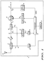
- FIG. 1 there is shown a schematic circuit diagram of a circuit for automatic tuning calibration of electronically tuned filters in a radio receiver in accordance with a preferred embodiment of the invention.
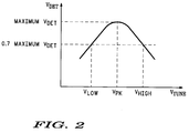
- FIG. 2 there is a representative graph of a detector voltage versus tuning voltage curve for a particular test signal (synthesizer frequency).
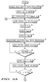
- FIG. 3 there is a flowchart representation of a method of automatic tuning calibration of electronically tuned filters in accordance with a preferred embodiment of the invention.
- FIG. 1 illustrates schematically the diagram of a circuit for automatic tuning calibration of electronically tuned filters.
- the approach can be applied in RF equipment such as transmitters, receivers, or test equipment, i.e., any application using electronically tuned filters and possessing programmable RF sources and microprocessor controlled systems.
- the FIG. 1 application represents the method and apparatus applied to the radio receiver 11.
- antenna 10 is coupled to filter 12.
- Filter 12 is coupled through amplifier 14 to junction 36.
- Junction 36 is coupled both through filter 16 to R port 38 of mixer 18 and through detector 26 to converter 24.
- Converter 24 is coupled to processor 22.
- Processor 22 is coupled through converter 28 to junction 34.
- Memory 23 is coupled to processor 22.
- Junction 34 is coupled to filter 12 and also to filter 16.
- Processor 22 is also coupled through synthesizer 20 to L port 40 of mixer 18. Processor 22 is also coupled through bias switch 30 to junction 32. Junction 32 is coupled to the I port 42 of mixer 18. Junction 32 serves as the intermediate frequency (IF) output.
- IF intermediate frequency
- Filters 12 and 16 in the preferred embodiment are to be essentially identical filters. Filters 12 and 16 exhibiting identical performance characteristics allows the tuning calibration measurements to test filter 16, but apply the tuning voltages resulting from the tuning calibration measurements to the receiver filter 12. Should the filters not be identical, or it be desirable to characterize the tuning characteristics of filter 12 directly, filter 12 may be calibrated in a manner similar to the calibration of filter 16.
- the FIG. 1 circuit automatically determines the correct tuning voltage for tuning the receiving tuning filter 12 in the following way.
- Processor 22 enables bias switch 30 to a bias (direct) current, i.e., I B , through junction 32 to the I port 42 of diode balanced mixer 18.
- Processor 22 simultaneously executes a program using synthesizer 20 to generate a test signal, i.e., a synthesizer signal at frequency F S .
- a test signal i.e., a synthesizer signal at frequency F S .
- R port 38 of mixer 18 is connected to L port 40 of mixer 18, test signal F S is input into filter 16.
- the test signal F S passes through filter 16 to junction 36, and then into detector 26.
- Processor 22 transmits a digital tuning voltage to converter 28.
- Converter 28 a digital-to-analog converter, creates an analog tuning voltage signal from the digital tuning voltage of processor 28 and applies the analog tuning voltage V T2 to junction 34 and, thus, to filter 16.
- the analog tuning voltage is also input into filter 12 as V T1 .
- the tuning voltages V T1 and V T2 are identical.
- Filter 16 produces an output based on the synthesizer signal at frequency F S and the tuning voltage V T2 input to filter 16.
- the filter 16 output is received by the detector 26, which produces a detected voltage, V DET , in response.
- Processor 22 sets the first synthesizer frequency, F S1 , to a first calibration frequency, i.e., the lowest filter frequency for both filters 12 and 16. While producing the fixed test signal, F S1 , processor 22 also produces the digital tuning voltage signal in steps.
- the stepped digital tuning voltage produces a range of analog tuning voltages from converter 28, which in turn produces a series of detected analog voltages, V DET , from detector 26.
- FIG. 2 illustrates what curve the detected voltage, V DET , versus tuning voltage, V T1 or V T2 , shown on the abscissa as V TUNE , might trace for filter 12 or filter 16.
- the detected voltage rises as the tuning voltage is increased, reaches a relative local maximum, and decreases.
- the FIG. 1 circuit processes the FIG. 2 information as follows.
- Processor 22 receiving a digital version of the detected voltage from detector 26 through converter 24, stores the detected voltage corresponding to each tuning step in the memory 23.
- the processor stores the tuning voltage corresponding to the maximum detected voltage as V PK .
- Processor 22 continues to step the tuning voltage until the detected voltage drops below a value of 0.7V PK . This value was chosen for the preferred embodiment but can be chosen differently, depending on the desired application and effect, without affecting the operation of the automatic filter calibration method.
- Processor 22 then examines previously stored detector voltages from tuning voltages less than V PK and defines the tuning voltage that precedes the first step where V DET was greater or equal to 0.7V PK as V LOW .
- V LOW is also stored in memory 23.
- V CORR is an empirical correction factor from a look-up table stored in memory 23, and represents a tuning voltage correction based on the particular filter shape and filter center frequency used. The use of V CORR allows the processor 22 to set a tuning voltage slightly off the passband center frequency to optimize for other considerations, such as stopband symmetry or maximum high side or low side rejection, etc., if so desired.
- the processor 22 stores V TS1 as the correct tuning voltage at frequency F S1 . (Depending on how narrow the band of filter 12 or 16, processor 22 could also calculate the tuning voltage using another algorithm, e.g., as the geometric mean of V LO and V HIGH .)
- Processor 22 sets a next calibration frequency, F S2 , i.e., a step up from the lowest filter frequency for both filters 12 and 16. While the synthesizer produces the fixed test signal, F S2 , processor 22 also produces the digital tuning voltage in steps. The stepped digital tuning voltage produces a range of analog tuning voltages from converter 28, which in turn produces another series of detected analog voltages, V DET , from detector 26 for the second test signal, F S2 . In the same manner described for determining V PK , V LOW , and V HIGH for the first test signal, F S1 , new V PK , V LOW , and V HIGH values are generated for F S2 by processor 22 and stored in memory 23.
- the same calibration process is repeated for test signals F S3 through F SN , with F SN being the highest usable frequency of the filters 12 and 16.
- the number of calibration iterations, N can be varied, depending on the tuning range and the linearity of the responses of filters 12 and 16 over that range.
- a correct tuning voltage, V TSi is therefore generated and stored for each test signal F Si throughout the usable frequencies of filters 12 and 16.
- the list, or table, of correct tuning voltages versus frequency stored in memory 23 can be used to calibrate filter 16 when operated as a receiver filter in FIG. 1.
- the antenna in FIG. 1 receives an external signal which is transmitted to filter 12.
- the correct tuning voltage for any operating frequency F X within the operational frequency limits of filter 12, i.e., from F S1 to F SN is calculated by linear interpolation by processor 22 using the two tuning voltage calibration points closest in frequency to F X .
- FIG. 3 illustrates the automatic filter tuning approach method applying to the circuit in FIG. 1.
- the bias switch 30 is enabled by the processor 22, as shown in box 50 of FIG. 3.
- the bias current I B is applied to mixer 18, as shown in box 52.
- Synthesizer 20 is programmed by processor 22 to produce a signal at the lowest usable frequency of filters 12 and 16.
- Synthesizer 20 produces a signal at frequency F S , illustrated in box 53.
- the synthesizer signal at frequency F S is transmitted to filter 16, as shown in box 54.
- Box 56 of FIG. 3 shows the filtering of the synthesizer signal, and boxes 58 and 60 describe detection and digitization, respectively, of the resulting detector voltage.
- Processor 22 reads and stores the digitized detector voltage V DET , as shown in box 62. Processor 22 also steps the tuning voltage to filter 16, as shown in box 64. If the detector voltage read for the current tuning voltage step is not the maximum detector voltage, box 66 transfers control to box 64 via the NO path and the system continues to step the filter tuning voltage to find the maximum voltage. If the detector voltage read for the current tuning voltage step is the maximum detector voltage, that maximum value is stored in the memory 23 as V PK , as shown by box 66 transferring control to box 67, proceeding on the YES path.
- the filter tuning voltage continues to be stepped to locate V HIGH , which is the tuning voltage for which the detected voltage has decreased from V PK to 0.7V PK . If the detected voltage V DET is not V HIGH , control is transferred from box 69 to box 68 via the NO path and the system continues stepping the tuning voltage. If, however, the current V DET is equal to V HIGH , then via the YES path, box 69 is taken to box 70 and V DET is stored in memory 23 as V HIGH , as shown in box 70.
- V LOW is determined by the processor 22 comparing previously stored V DET values in memory 23 with V PK .
- V LOW is set equal to the tuning voltage that precedes the first tuning voltage step where V DET was greater or equal to 0.7V PK , as shown in box 71.
- the empirical correction factor V CORR is read from the memory 23 as shown in box 72, and, as shown in box 74, processor 22 calculates and stores the tuning voltage value for the particular synthesizer frequency F Si using equation 1.
- control is transferred from box 76 via the NO path to box 78 where a new synthesizer frequency F S is generated. Control is transferred to box 54, and the F S signal at the new synthesizer frequency is sent to filter 16.
- the system repeats e steps shown in the flowchart boxes to calculate the tuning voltage V TS for the new F S .
- F S is the highest usable filter 16 frequency
- control is transferred from box 76 to box 80 via the YES path, and the tuning voltage versus frequency table is complete and stored in memory 23.
- F X can be looked up in the tuning voltage table, as shown in box 84.
- linear interpolation can be used to locate the proper tuning voltage for F X between any two frequency values in the table.
- the tuning voltage corresponding to the operating frequency F X can then be used to calibrate filter 16 (or filter 12), as shown in box 88. The process is complete.
- the method and apparatus for automatic tuning calibration of electronically tuned filters requires relatively few components, is relatively inexpensive, and does not require adjustments at the factory.
- the approach is applicable to RF equipment such as transmitters, receivers, or test equipment that require electronically tuned filters and possess programmable RF sources and microprocessor-controlled systems. The approach reduces the cost of the filters and provides precise tuning of very narrow bandwidth filters that might not otherwise be feasible due to the high tracking accuracy required.
Abstract
Description
- This invention relates in general to the field of tuning calibration, and in particular to the automatic tuning calibration of electronically tuned filters.
- Electronically tuned radio frequency (RF) filters such as those implemented with varactors produce varying tuning characteristics, e.g., frequency versus voltage variations, that are a function of a number of variables. Varying tuning characteristics can arise from variability in component tolerances, printed wiring board dimensions and the dielectric constant of the board material, stray inductance and capacitance variations due to component and shield or ground plane placement.
- Many equipment designs in which electronically tuned filters are used contain microprocessor controllers and non-volatile memory capability. Typical filter calibration techniques do not take advantage of these additional components in addressing the filter calibration problem in electronically tuned filters.
- Among typical approaches used to calibrate electronically tuned filters are adjustable RF components used to "trim" the filter to track a predetermined tuning curve, adjustable or select-in-test components in an analog tracking circuit to interface a standard voltage versus frequency curve to the individual characteristics of the filter, and components with very accurate value tolerances. These techniques are expensive in terms of test labor required and/or component cost.
- Another approach to address electronically tuned filter calibration is an active approach which measures the phase shift between an applied test signal and the filter output and which provides a unique null output indicating correct tuning of the filter. This active servo loop technique is relatively elaborate and more expensive, however, requiring several directional couplers and a phase detector and higher signal levels for proper operation as a result.
- A need exists, therefore, for a method and apparatus for automatic tuning calibration of electronically tuned filters which requires relatively few components, is relatively inexpensive, and does not require adjustments at the factory. The approach should be applicable in RF equipment such as transmitters, receivers, or test equipment that require electronically tuned filters and include programmable RF sources and microprocessor-controlled systems. The approach should reduce the cost of the filters and provide precise tuning of very narrow bandwidth filters that might not otherwise be feasible due to the high tracking accuracy required.
- Accordingly, it is an advantage of the present invention to provide a new and improved method and apparatus for automatic tuning calibration of electronically tuned filters which takes advantage of programmable RF sources and microprocessor-controlled systems. It is an additional advantage that the method and apparatus for automatic tuning calibration is generally applicable to transmitters, receivers, and/or test equipment, yet requires relatively few components and is relatively inexpensive. It is still further an advantage of the present invention the method and apparatus for automatic tuning calibration of electronically tuned filters provides precise tuning of very narrow bandwidth filters that might not otherwise be feasible due to the high tracking accuracy required.
- To achieve these advantages, a method and apparatus for automatic tuning calibration of electronically tuned filters is contemplated which comprises a programmable frequency generator for producing a calibration frequency signal, a filter for filtering the calibration frequency signal, a detector for producing a detector voltage, a processor for programming the frequency generator to specific test frequencies and for producing a stepped filter tuning voltage and storing the detector voltage in response to the stepped filter tuning voltage, and a converter for digital-to-analog conversion of the stepped filter tuning voltage.
- Calibration frequency signal versus tuning voltage responses are stored for a number of calibration iterations within the usable range of the filter. The calibration frequency signal versus tuning voltage table is then used to determine the correct tuning voltage for the filter for any frequency within the usable range of the filter.
- The above and other features and advantages of the present invention will be better understood from the following detailed description taken in conjunction with the accompanying drawings.
- In FIG. 1, there is shown a schematic circuit diagram of a circuit for automatic tuning calibration of electronically tuned filters in a radio receiver in accordance with a preferred embodiment of the invention.
- In FIG. 2, there is a representative graph of a detector voltage versus tuning voltage curve for a particular test signal (synthesizer frequency).
- In FIG. 3, there is a flowchart representation of a method of automatic tuning calibration of electronically tuned filters in accordance with a preferred embodiment of the invention.
- FIG. 1 illustrates schematically the diagram of a circuit for automatic tuning calibration of electronically tuned filters. The approach can be applied in RF equipment such as transmitters, receivers, or test equipment, i.e., any application using electronically tuned filters and possessing programmable RF sources and microprocessor controlled systems. The FIG. 1 application represents the method and apparatus applied to the radio receiver 11.
- In FIG. 1,
antenna 10 is coupled to filter 12.Filter 12 is coupled throughamplifier 14 tojunction 36.Junction 36 is coupled both throughfilter 16 toR port 38 ofmixer 18 and throughdetector 26 to converter 24.Converter 24 is coupled toprocessor 22.Processor 22 is coupled throughconverter 28 tojunction 34.Memory 23 is coupled toprocessor 22.Junction 34 is coupled to filter 12 and also to filter 16. -
Processor 22 is also coupled throughsynthesizer 20 toL port 40 ofmixer 18.Processor 22 is also coupled throughbias switch 30 tojunction 32.Junction 32 is coupled to theI port 42 ofmixer 18.Junction 32 serves as the intermediate frequency (IF) output. -
Filters Filters filter 16, but apply the tuning voltages resulting from the tuning calibration measurements to thereceiver filter 12. Should the filters not be identical, or it be desirable to characterize the tuning characteristics offilter 12 directly,filter 12 may be calibrated in a manner similar to the calibration offilter 16. - In operation, the FIG. 1 circuit automatically determines the correct tuning voltage for tuning the receiving
tuning filter 12 in the following way.Processor 22 enablesbias switch 30 to a bias (direct) current, i.e., IB, throughjunction 32 to the Iport 42 of diode balancedmixer 18.Mixer 18, responding to the bias current at the Iport 42, connectsR port 38 toL port 40 ofmixer 18. -
Processor 22 simultaneously executes aprogram using synthesizer 20 to generate a test signal, i.e., a synthesizer signal at frequency FS. When Rport 38 ofmixer 18 is connected toL port 40 ofmixer 18, test signal FS is input intofilter 16. The test signal FS passes throughfilter 16 tojunction 36, and then intodetector 26. -
Processor 22 transmits a digital tuning voltage to converter 28. Converter 28, a digital-to-analog converter, creates an analog tuning voltage signal from the digital tuning voltage ofprocessor 28 and applies the analog tuning voltage VT2 tojunction 34 and, thus, to filter 16. Atjunction 34, the analog tuning voltage is also input intofilter 12 as VT1. The tuning voltages VT1 and VT2 are identical. -
Filter 16 produces an output based on the synthesizer signal at frequency FS and the tuning voltage VT2 input tofilter 16. Thefilter 16 output is received by thedetector 26, which produces a detected voltage, VDET, in response. -
Processor 22 sets the first synthesizer frequency, FS1, to a first calibration frequency, i.e., the lowest filter frequency for bothfilters processor 22 also produces the digital tuning voltage signal in steps. The stepped digital tuning voltage produces a range of analog tuning voltages fromconverter 28, which in turn produces a series of detected analog voltages, VDET, fromdetector 26. - FIG. 2 illustrates what curve the detected voltage, VDET, versus tuning voltage, VT1 or VT2, shown on the abscissa as VTUNE, might trace for
filter 12 orfilter 16. The detected voltage rises as the tuning voltage is increased, reaches a relative local maximum, and decreases. The local maximum occurs when the tuning voltage VTUNE = VPK, and VLOW and VHIGH are defined as the tuning voltages giving rise to detector voltage values of 0.7VDET maximum. - The FIG. 1 circuit processes the FIG. 2 information as follows.
Processor 22, receiving a digital version of the detected voltage fromdetector 26 throughconverter 24, stores the detected voltage corresponding to each tuning step in thememory 23. The processor stores the tuning voltage corresponding to the maximum detected voltage as VPK. Processor 22 continues to step the tuning voltage until the detected voltage drops below a value of 0.7VPK. This value was chosen for the preferred embodiment but can be chosen differently, depending on the desired application and effect, without affecting the operation of the automatic filter calibration method.Processor 22 stores the tuning voltage corresponding to VDET = 0.7VPK as VHIGH inmemory 23.Processor 22 then examines previously stored detector voltages from tuning voltages less than VPK and defines the tuning voltage that precedes the first step where VDET was greater or equal to 0.7VPK as VLOW. VLOW is also stored inmemory 23. -
Processor 22 in this preferred embodiment using a relatively narrow bandwidth filter then calculates the correct tuning voltage for frequency FS1 using the equation:

where i = 1. VCORR is an empirical correction factor from a look-up table stored inmemory 23, and represents a tuning voltage correction based on the particular filter shape and filter center frequency used. The use of VCORR allows theprocessor 22 to set a tuning voltage slightly off the passband center frequency to optimize for other considerations, such as stopband symmetry or maximum high side or low side rejection, etc., if so desired. Theprocessor 22 stores VTS1 as the correct tuning voltage at frequency FS1. (Depending on how narrow the band offilter processor 22 could also calculate the tuning voltage using another algorithm, e.g., as the geometric mean of VLO and VHIGH.) -
Processor 22 sets a next calibration frequency, FS2, i.e., a step up from the lowest filter frequency for bothfilters processor 22 also produces the digital tuning voltage in steps. The stepped digital tuning voltage produces a range of analog tuning voltages fromconverter 28, which in turn produces another series of detected analog voltages, VDET, fromdetector 26 for the second test signal, FS2. In the same manner described for determining VPK, VLOW, and VHIGH for the first test signal, FS1, new VPK, VLOW, and VHIGH values are generated for FS2 byprocessor 22 and stored inmemory 23. - The same calibration process is repeated for test signals FS3 through FSN, with FSN being the highest usable frequency of the
filters filters filters - The list, or table, of correct tuning voltages versus frequency stored in
memory 23 can be used to calibratefilter 16 when operated as a receiver filter in FIG. 1. The antenna in FIG. 1 receives an external signal which is transmitted to filter 12. The correct tuning voltage for any operating frequency FX within the operational frequency limits offilter 12, i.e., from FS1 to FSN, is calculated by linear interpolation byprocessor 22 using the two tuning voltage calibration points closest in frequency to FX. - FIG. 3 illustrates the automatic filter tuning approach method applying to the circuit in FIG. 1. The
bias switch 30 is enabled by theprocessor 22, as shown inbox 50 of FIG. 3. The bias current IB is applied tomixer 18, as shown inbox 52.Synthesizer 20 is programmed byprocessor 22 to produce a signal at the lowest usable frequency offilters Synthesizer 20 produces a signal at frequency FS, illustrated inbox 53. The synthesizer signal at frequency FS is transmitted to filter 16, as shown inbox 54.Box 56 of FIG. 3 shows the filtering of the synthesizer signal, andboxes -
Processor 22 reads and stores the digitized detector voltage VDET, as shown inbox 62.Processor 22 also steps the tuning voltage to filter 16, as shown inbox 64. If the detector voltage read for the current tuning voltage step is not the maximum detector voltage,box 66 transfers control tobox 64 via the NO path and the system continues to step the filter tuning voltage to find the maximum voltage. If the detector voltage read for the current tuning voltage step is the maximum detector voltage, that maximum value is stored in thememory 23 as VPK, as shown bybox 66 transferring control tobox 67, proceeding on the YES path. - In
box 68, the filter tuning voltage continues to be stepped to locate VHIGH, which is the tuning voltage for which the detected voltage has decreased from VPK to 0.7VPK. If the detected voltage VDET is not VHIGH, control is transferred frombox 69 tobox 68 via the NO path and the system continues stepping the tuning voltage. If, however, the current VDET is equal to VHIGH, then via the YES path,box 69 is taken tobox 70 and VDET is stored inmemory 23 as VHIGH, as shown inbox 70. - VLOW is determined by the
processor 22 comparing previously stored VDET values inmemory 23 with VPK. VLOW is set equal to the tuning voltage that precedes the first tuning voltage step where VDET was greater or equal to 0.7VPK, as shown inbox 71. - The empirical correction factor VCORR is read from the
memory 23 as shown inbox 72, and, as shown inbox 74,processor 22 calculates and stores the tuning voltage value for the particular synthesizer frequency FSi using equation 1. - If the current FS is not the highest
usable filter 16 frequency, control is transferred frombox 76 via the NO path to box 78 where a new synthesizer frequency FS is generated. Control is transferred tobox 54, and the FS signal at the new synthesizer frequency is sent to filter 16. The system repeats e steps shown in the flowchart boxes to calculate the tuning voltage VTS for the new FS. - If FS is the highest
usable filter 16 frequency, control is transferred frombox 76 tobox 80 via the YES path, and the tuning voltage versus frequency table is complete and stored inmemory 23. For any operational frequency FX as shown inbox 82, FX can be looked up in the tuning voltage table, as shown inbox 84. As shown inbox 86, linear interpolation can be used to locate the proper tuning voltage for FX between any two frequency values in the table. The tuning voltage corresponding to the operating frequency FX can then be used to calibrate filter 16 (or filter 12), as shown inbox 88. The process is complete. - Thus, there has been described a method and apparatus for automatic tuning calibration of electronically tuned filters which overcomes specific problems and accomplishes certain advantages relative to prior art methods and mechanisms. The improvements are significant. The method and apparatus for automatic tuning calibration of electronically tuned filters requires relatively few components, is relatively inexpensive, and does not require adjustments at the factory. The approach is applicable to RF equipment such as transmitters, receivers, or test equipment that require electronically tuned filters and possess programmable RF sources and microprocessor-controlled systems. The approach reduces the cost of the filters and provides precise tuning of very narrow bandwidth filters that might not otherwise be feasible due to the high tracking accuracy required.
- Thus, there has also been provided, in accordance with an embodiment of the invention, a method and apparatus for automatic tuning calibration of electronically tuned filters which overcomes specific problems and accomplishes certain advantages and which fully satisfies the aims and advantages set forth above. While the invention has been described in conjunction with a specific embodiment, many alternatives, modifications, and variations will be apparent to those of ordinary skill in the art in light of the foregoing description. Accordingly, the invention is intended to embrace all such alternatives, modifications, and variations as fall within the spirit and broad scope of the appended claims.
Claims (10)
- An automatic tuning calibrator (11) for electronically tuned filters (12, 16) comprising:
programmable frequency generator means (20, 18, 30) for producing (53) a calibration frequency signal;
filter means (16) for filtering (54) the calibration frequency signal, the filter means (16) coupled to the frequency generator means (20, 18, 30);
detector means (26, 24) for producing (58) a detector voltage (VDET), the detector means (26, 24) coupled to the filter means (16);
processor means (22, 23) for producing (64, 66) a stepped filter tuning voltage (VT1, VT2) and for storing (67) the detector voltage (VDET) in response to the stepped filter tuning voltage (VT1, VT2), the processor means (22, 23) coupled to the detector means (26, 24) and to the frequency generator means (20, 18, 30); and
converter means (28) for digital-to-analog conversion of the stepped filter tuning voltage (VT1, VT2), the converter means (28) coupled to the processor means (22, 23) and to the filter means (16). - An automatic tuning calibrator (11) as claimed in claim 1, wherein the frequency generator means (20, 18, 30) comprises:
synthesizer means (20) for producing (53) the calibration frequency signal;
mixer means (18) for connecting the synthesizer means (20) to the filter means (16), the mixer means (18) coupled to the synthesizer means (20) and to the filter means (16); and
bias switch means (30) for enabling (50, 52) the mixer means (18), the bias switch means (30) coupled to the mixer means (18) and to the processor means (22, 23). - An automatic tuning calibrator (11) as claimed in claim 2, wherein the detector means (26, 24) comprises:
analog voltage detector means (26) for detecting (58) the filtered calibration frequency signal and for producing (58) an analog detector voltage output, the analog voltage detector means (26) coupled to the filter means (16); and
analog-to-digital converter means (24) for producing (60) the detector voltage output from the analog voltage output, the analog-to-digital converter means (24) coupled to the analog voltage detector means (26) and to the processor means (22, 23). - An automatic tuning calibrator (11) as claimed in claim 2, wherein the processor means (22, 23) comprises:
storage means (23) for recording (62) the digitized detector voltage output; and
microprocessor means (22) for enabling (50, 52) the bias switch means (18), for programming (53, 64, 68) the synthesizer means (20), for producing (64, 68) a stepped filter tuning voltage (VT1, VT2), and for determining (64-88) a calculated tuning voltage (VTS1) from the detector voltage (VDET), the microprocessor means (22) coupled to the storage means (23). - An automatic tuning calibrator (11) as claimed in claim 4, wherein the storage means (23) comprises non-volatile memory (23).
- An automatic tuning calibrator (11) for tuning electronically tuned filters (12, 16) in a radio receiver (11), the automatic tuning calibrator (11) comprising:
programmable frequency generator means (20, 18, 30) for producing (53) a calibration frequency signal;
first filter means (16) for producing (54) a filtered calibration frequency signal from the calibration frequency signal, the first filter means (16) coupled to the frequency generator means (20, 18, 30);
detector means (26, 24) for producing (58, 60) a detector voltage (VDET), the detector means (26, 24) coupled to the first filter means (16);
processor means (22, 23) for producing (64, 68) a stepped filter tuning voltage (VT1, VT2) and for storing (67, 70) the detector voltage (VDET) in response to the stepped filter tuning voltage (VT1, VT2), the processor means (22, 23) coupled to the detector means (26, 24) and to the frequency generator means (20, 18, 30);
converter means (28) for digital-to-analog conversion of the stepped filter tuning voltage (VT1, VT2), the converter means (28) coupled to the processor means (22, 23) and to the first filter means (16); and
radio receiver means (10, 12, 14) for receiving an operating frequency signal, the radio receiver means (10, 12, 14) coupled to the first filter means (16), to the detector means (26, 24), and to the converter means (28). - An automatic tuning calibrator (11) as claimed in claim 6, wherein the frequency generator means (20, 18, 30) comprises:
synthesizer means (20) for producing (53) the calibration frequency signal;
mixer means (18) for connecting the synthesizer to the first filter means (16), the mixer means (18) coupled to the synthesizer means (20) and to the first filter means (16); and
bias switch means (30) for enabling (50, 52) the mixer means (18), the bias switch means (30) coupled to the mixer means (18) and the processor means (22, 23). - An automatic tuning calibrator (11) as claimed in claim 6, wherein the detector means (26, 24) comprises:
analog voltage detector means (26) for detecting (58) the filtered calibration frequency signal and for producing an analog voltage output, the analog voltage detector means (26) coupled to the first filter means (16); and
analog-to-digital converter means (24) for producing (60) the detector voltage output from the analog voltage output, the analog-to-digital converter means (24) coupled to the analog voltage detector means (26) and to the processor means (22, 23). - An automatic tuning calibrator (11) as claimed in claim 7, wherein the processor means (22, 23) comprises:
non-volatile memory (23) for recording the detector voltage (VDET); and
microprocessor means (22) for enabling (50, 52) the bias switch means (18), for programming (53) the synthesizer means (20), for producing ( 64, 68) a stepped filter tuning voltage (VT1, VT2), and for determining (64-88) a calculated tuning voltage (VTS1) from the detector voltage (VDET), the microprocessor means (22) coupled to the storage means (23). - A method for automatic tuning calibration of electronically tuned filters (12, 16) comprising the steps of:
producing (53) a calibration frequency signal in a programmable frequency generator (20, 18, 30);
producing (56) a filtered calibration frequency signal from the calibration frequency signal in a first filter (16);
producing (58) a detector voltage (VDET) in a detector (26, 24);
producing (64, 68) a stepped filter tuning voltage (VT1, VT2) in a processor (22, 23);
storing (67, 70) the detector voltage (VDET) in response to the stepped filter tuning voltage (VT1, VT2) in the processor (22, 23); and
calculating (74-88) a filter tuning voltage (VTS1) from the detector voltage (VDET) in the processor (22, 23).
Applications Claiming Priority (2)
| Application Number | Priority Date | Filing Date | Title |
|---|---|---|---|
| US78717291A | 1991-11-04 | 1991-11-04 | |
| US787172 | 1991-11-04 |
Publications (2)
| Publication Number | Publication Date |
|---|---|
| EP0540908A1 true EP0540908A1 (en) | 1993-05-12 |
| EP0540908B1 EP0540908B1 (en) | 1997-01-08 |
Family
ID=25140629
Family Applications (1)
| Application Number | Title | Priority Date | Filing Date |
|---|---|---|---|
| EP92117504A Expired - Lifetime EP0540908B1 (en) | 1991-11-04 | 1992-10-14 | Method and apparatus for automatic tuning calibration of electronically tuned filters |
Country Status (4)
| Country | Link |
|---|---|
| US (1) | US5822687A (en) |
| EP (1) | EP0540908B1 (en) |
| JP (1) | JPH05327418A (en) |
| DE (1) | DE69216554T2 (en) |
Cited By (2)
| Publication number | Priority date | Publication date | Assignee | Title |
|---|---|---|---|---|
| EP0629045B1 (en) * | 1993-06-07 | 2000-03-22 | MIVAR S.r.l. | Tuning device for a receiver of radioelectric signals with coils obtained by printing |
| GB2349525A (en) * | 1999-04-21 | 2000-11-01 | Infineon Technologies Inc | A receiver with varactor filters before the mixer which are controlled in such a way as to compensate for non-linearity |
Families Citing this family (36)
| Publication number | Priority date | Publication date | Assignee | Title |
|---|---|---|---|---|
| JPH09289467A (en) * | 1996-04-23 | 1997-11-04 | Oki Electric Ind Co Ltd | High-frequency receiving circuit of mobile communication equipment |
| JPH1013181A (en) * | 1996-06-21 | 1998-01-16 | Nec Corp | System for automatic matching if filter |
| US6014554A (en) * | 1997-09-30 | 2000-01-11 | Lucent Technologies, Inc. | Method and apparatus for tuning analog filters |
| US6088581A (en) * | 1998-03-27 | 2000-07-11 | Motorola, Inc. | Method and apparatus for reducing amplitude modulated interference in a receiver |
| US6278953B1 (en) * | 1998-10-20 | 2001-08-21 | Lucent Technologies, Inc. | Automated alignment system |
| JP2001156591A (en) * | 1999-11-25 | 2001-06-08 | Alps Electric Co Ltd | Active filter and its band adjustment method |
| JP2001218120A (en) * | 2000-01-02 | 2001-08-10 | Alps Electric Co Ltd | Frequency conversion circuit for cable television transmitter |
| US7050778B1 (en) * | 2000-09-18 | 2006-05-23 | Broadcom Corporation | Direct conversion turner |
| US7054606B1 (en) * | 2001-09-21 | 2006-05-30 | Lsi Logic Corporation | Digitally calibrated narrowband filter with analog channel compensation |
| EP1440539A4 (en) * | 2001-09-27 | 2009-08-26 | Broadcom Corp | Highly integrated media access control |
| US6915114B2 (en) * | 2002-05-07 | 2005-07-05 | Broadcom, Corp. | Direct tuning of embedded integrated circuit components |
| US20060063503A1 (en) * | 2002-06-17 | 2006-03-23 | Koninklikle Phillips Electronics Nv | Receiver and tuner with electronically tuned filter |
| JP2004088609A (en) * | 2002-08-28 | 2004-03-18 | Sharp Corp | Frequency converter |
| DE10321200B3 (en) * | 2003-05-12 | 2005-02-03 | Infineon Technologies Ag | Apparatus and method for calibrating R / C filter circuits |
| US20040230997A1 (en) * | 2003-05-13 | 2004-11-18 | Broadcom Corporation | Single-chip cable set-top box |
| US7336939B2 (en) * | 2003-05-21 | 2008-02-26 | Broadcom Corporation | Integrated tracking filters for direct conversion and low-IF single conversion broadband filters |
| US20050040909A1 (en) * | 2003-08-20 | 2005-02-24 | Waight Matthew Glenn | Broadband integrated digitally tunable filters |
| US7702306B2 (en) * | 2003-08-28 | 2010-04-20 | Broadcom Corporation | Apparatus and method for local oscillator calibration in mixer circuits |
| US7587175B2 (en) * | 2003-10-20 | 2009-09-08 | Broadcom Corporation | Radio frequency unit analog level detector and feedback control system |
| JP4294455B2 (en) * | 2003-12-03 | 2009-07-15 | パイオニア株式会社 | Receiving machine |
| US7894790B2 (en) * | 2004-04-02 | 2011-02-22 | Broadcom Corporation | Dual conversion receiver with reduced harmonic interference |
| US8578434B2 (en) * | 2004-05-21 | 2013-11-05 | Broadcom Corporation | Integrated cable modem |
| US8732788B2 (en) * | 2004-05-21 | 2014-05-20 | Broadcom Corporation | Integrated set-top box |
| US8239914B2 (en) * | 2004-07-22 | 2012-08-07 | Broadcom Corporation | Highly integrated single chip set-top box |
| ATE524879T1 (en) * | 2005-07-21 | 2011-09-15 | Telegent Systems Inc | TUNABLE FILTER WITH INCREASED BIAS AND RUNTIME CALIBRATION |
| ATE453961T1 (en) * | 2005-10-27 | 2010-01-15 | Nxp Bv | CALIBRATION DEVICE AND PROCESS WITH FORWARD/REVERSE MECHANISM FOR A BANDPASS FILTER |
| US7995981B2 (en) * | 2005-10-31 | 2011-08-09 | Silicon Laboratories Inc. | Receiver with image rejection calibration at an undesired picture carrier and method therefor |
| US20070294738A1 (en) * | 2006-06-16 | 2007-12-20 | Broadcom Corporation | Single chip cable set-top box supporting DOCSIS set-top Gateway (DSG) protocol and high definition advanced video codec (HD AVC) decode |
| US7577413B2 (en) * | 2006-09-19 | 2009-08-18 | Silicon Laboratories, Inc. | Method and apparatus for calibrating a filter of a receiver |
| US7660566B2 (en) * | 2006-09-29 | 2010-02-09 | Visteon Global Technologies, Inc. | System for creating a programmable tuning voltage |
| US7937058B2 (en) * | 2006-10-18 | 2011-05-03 | Freescale Semiconductor, Inc. | Controlling the bandwidth of an analog filter |
| US20090163162A1 (en) * | 2007-12-19 | 2009-06-25 | Hoffman Stephen W | Direct conversion receiving architecture with an integrated tuner self alignment function |
| JP4968146B2 (en) * | 2008-03-31 | 2012-07-04 | ソニー株式会社 | Broadcast signal receiver, reception control method thereof, and IC |
| US9059774B2 (en) * | 2008-10-07 | 2015-06-16 | Nxp, B.V. | Reduction method and apparatus |
| US20100306814A1 (en) * | 2009-05-26 | 2010-12-02 | Broadcom Corporation | Integrated Set-Top Box with Daisy-Chaining |
| WO2010138198A1 (en) * | 2009-05-29 | 2010-12-02 | Thomson Licensing | Fast cycle slip detection and correction |
Citations (5)
| Publication number | Priority date | Publication date | Assignee | Title |
|---|---|---|---|---|
| US4334323A (en) * | 1980-09-08 | 1982-06-08 | Zenith Radio Corporation | Self tracking tuner |
| EP0109661A1 (en) * | 1982-11-20 | 1984-05-30 | Deutsche Thomson-Brandt GmbH | Tuner for a communication apparatus |
| EP0116350A1 (en) * | 1983-02-04 | 1984-08-22 | Deutsche Thomson-Brandt GmbH | Tunig unit for communication apparatus |
| EP0119561A2 (en) * | 1983-03-11 | 1984-09-26 | Deutsche Thomson-Brandt GmbH | Method of tuning the resonant circuits of a radio receiver |
| EP0208470A2 (en) * | 1985-07-02 | 1987-01-14 | Matsushita Electric Industrial Co., Ltd. | Signal receiver with tuning circuits |
Family Cites Families (3)
| Publication number | Priority date | Publication date | Assignee | Title |
|---|---|---|---|---|
| US4368541A (en) * | 1980-06-30 | 1983-01-11 | Evans Robert M | Multiplexing arrangement for a plurality of voltage controlled filters |
| US5031131A (en) * | 1988-11-14 | 1991-07-09 | Eaton Corporation | Direct digital synthesizer |
| US5101509A (en) * | 1990-09-14 | 1992-03-31 | Ford Motor Company | Rf filter alignment using digital processor clock |
-
1992
- 1992-10-14 EP EP92117504A patent/EP0540908B1/en not_active Expired - Lifetime
- 1992-10-14 DE DE69216554T patent/DE69216554T2/en not_active Expired - Lifetime
- 1992-10-27 JP JP4311323A patent/JPH05327418A/en active Pending
-
1993
- 1993-08-23 US US08/110,233 patent/US5822687A/en not_active Expired - Lifetime
Patent Citations (5)
| Publication number | Priority date | Publication date | Assignee | Title |
|---|---|---|---|---|
| US4334323A (en) * | 1980-09-08 | 1982-06-08 | Zenith Radio Corporation | Self tracking tuner |
| EP0109661A1 (en) * | 1982-11-20 | 1984-05-30 | Deutsche Thomson-Brandt GmbH | Tuner for a communication apparatus |
| EP0116350A1 (en) * | 1983-02-04 | 1984-08-22 | Deutsche Thomson-Brandt GmbH | Tunig unit for communication apparatus |
| EP0119561A2 (en) * | 1983-03-11 | 1984-09-26 | Deutsche Thomson-Brandt GmbH | Method of tuning the resonant circuits of a radio receiver |
| EP0208470A2 (en) * | 1985-07-02 | 1987-01-14 | Matsushita Electric Industrial Co., Ltd. | Signal receiver with tuning circuits |
Cited By (3)
| Publication number | Priority date | Publication date | Assignee | Title |
|---|---|---|---|---|
| EP0629045B1 (en) * | 1993-06-07 | 2000-03-22 | MIVAR S.r.l. | Tuning device for a receiver of radioelectric signals with coils obtained by printing |
| GB2349525A (en) * | 1999-04-21 | 2000-11-01 | Infineon Technologies Inc | A receiver with varactor filters before the mixer which are controlled in such a way as to compensate for non-linearity |
| GB2349525B (en) * | 1999-04-21 | 2004-03-24 | Infineon Technologies Inc | Oscillating circuits |
Also Published As
| Publication number | Publication date |
|---|---|
| DE69216554T2 (en) | 1997-07-10 |
| JPH05327418A (en) | 1993-12-10 |
| US5822687A (en) | 1998-10-13 |
| EP0540908B1 (en) | 1997-01-08 |
| DE69216554D1 (en) | 1997-02-20 |
Similar Documents
| Publication | Publication Date | Title |
|---|---|---|
| EP0540908B1 (en) | Method and apparatus for automatic tuning calibration of electronically tuned filters | |
| US5281931A (en) | On-chip self-tuning filter system | |
| US4726071A (en) | Microprocessor controlled self-tuning resonant cavity and method | |
| US5101509A (en) | Rf filter alignment using digital processor clock | |
| EP0519145B1 (en) | Electrically tuned RF receiver, apparatus and method therefor | |
| EP1376853B1 (en) | Apparatus and method for tuning a filter | |
| US5335362A (en) | Method of tuning and compensating the received signal strength indicator in a radio telephone | |
| JPH0210604B2 (en) | ||
| US5678211A (en) | Television tuning apparatus | |
| US4510454A (en) | Apparatus for digitally controlled calibration of frequency response of amplifiers | |
| US5524288A (en) | Tuning of a radio receiver | |
| US4956711A (en) | Automatic balancing system for communications receiver apparatus | |
| EP0239219B1 (en) | High power systems | |
| US4758783A (en) | Compensation network for compensating the frequency response of a spectrum analyzer | |
| US6408167B1 (en) | Radio device including a receiver and method of adjusting one of the high-frequency amplifier stages of a receiver | |
| US4245350A (en) | Automatic gain control system for direct-access television receiver | |
| JPS62210719A (en) | Electronic tuner | |
| US2777953A (en) | System for calibrating oscillators | |
| EP1056204A1 (en) | Tunable RF filter with image trap | |
| EP0273031B1 (en) | Characterized fast tuning control for a television system | |
| US6188970B1 (en) | Method of calibrating a multistage selective amplifier | |
| US4604571A (en) | Circuit for the determination of voltage extrema | |
| US3947772A (en) | AFC tuning circuit | |
| JPH0434576Y2 (en) | ||
| US4906950A (en) | Time-frequency multiplexing system for correcting output amplitude of a tuned circuit due to impedance drift |
Legal Events
| Date | Code | Title | Description |
|---|---|---|---|
| PUAI | Public reference made under article 153(3) epc to a published international application that has entered the european phase |
Free format text: ORIGINAL CODE: 0009012 |
|
| AK | Designated contracting states |
Kind code of ref document: A1 Designated state(s): DE FR GB |
|
| 17P | Request for examination filed |
Effective date: 19930730 |
|
| 17Q | First examination report despatched |
Effective date: 19950616 |
|
| GRAG | Despatch of communication of intention to grant |
Free format text: ORIGINAL CODE: EPIDOS AGRA |
|
| GRAH | Despatch of communication of intention to grant a patent |
Free format text: ORIGINAL CODE: EPIDOS IGRA |
|
| GRAH | Despatch of communication of intention to grant a patent |
Free format text: ORIGINAL CODE: EPIDOS IGRA |
|
| GRAA | (expected) grant |
Free format text: ORIGINAL CODE: 0009210 |
|
| AK | Designated contracting states |
Kind code of ref document: B1 Designated state(s): DE FR GB |
|
| REF | Corresponds to: |
Ref document number: 69216554 Country of ref document: DE Date of ref document: 19970220 |
|
| ET | Fr: translation filed | ||
| PLBE | No opposition filed within time limit |
Free format text: ORIGINAL CODE: 0009261 |
|
| STAA | Information on the status of an ep patent application or granted ep patent |
Free format text: STATUS: NO OPPOSITION FILED WITHIN TIME LIMIT |
|
| 26N | No opposition filed | ||
| REG | Reference to a national code |
Ref country code: GB Ref legal event code: 732E |
|
| REG | Reference to a national code |
Ref country code: GB Ref legal event code: IF02 |
|
| PGFP | Annual fee paid to national office [announced via postgrant information from national office to epo] |
Ref country code: DE Payment date: 20091028 Year of fee payment: 18 |
|
| PGFP | Annual fee paid to national office [announced via postgrant information from national office to epo] |
Ref country code: GB Payment date: 20091026 Year of fee payment: 18 Ref country code: FR Payment date: 20091029 Year of fee payment: 18 |
|
| GBPC | Gb: european patent ceased through non-payment of renewal fee |
Effective date: 20101014 |
|
| PG25 | Lapsed in a contracting state [announced via postgrant information from national office to epo] |
Ref country code: FR Free format text: LAPSE BECAUSE OF NON-PAYMENT OF DUE FEES Effective date: 20101102 |
|
| REG | Reference to a national code |
Ref country code: FR Ref legal event code: ST Effective date: 20110630 |
|
| PG25 | Lapsed in a contracting state [announced via postgrant information from national office to epo] |
Ref country code: GB Free format text: LAPSE BECAUSE OF NON-PAYMENT OF DUE FEES Effective date: 20101014 |
|
| REG | Reference to a national code |
Ref country code: DE Ref legal event code: R119 Ref document number: 69216554 Country of ref document: DE Effective date: 20110502 |
|
| PG25 | Lapsed in a contracting state [announced via postgrant information from national office to epo] |
Ref country code: DE Free format text: LAPSE BECAUSE OF NON-PAYMENT OF DUE FEES Effective date: 20110502 |