EP0540347B1 - Motion detection circuit for high definition television picture signal based on the muse system - Google Patents
Motion detection circuit for high definition television picture signal based on the muse system Download PDFInfo
- Publication number
- EP0540347B1 EP0540347B1 EP92309955A EP92309955A EP0540347B1 EP 0540347 B1 EP0540347 B1 EP 0540347B1 EP 92309955 A EP92309955 A EP 92309955A EP 92309955 A EP92309955 A EP 92309955A EP 0540347 B1 EP0540347 B1 EP 0540347B1
- Authority
- EP
- European Patent Office
- Prior art keywords
- horizontal
- filter means
- signal
- circuit
- coupled
- Prior art date
- Legal status (The legal status is an assumption and is not a legal conclusion. Google has not performed a legal analysis and makes no representation as to the accuracy of the status listed.)
- Expired - Lifetime
Links
Images

Classifications
-
- H—ELECTRICITY
- H04—ELECTRIC COMMUNICATION TECHNIQUE
- H04N—PICTORIAL COMMUNICATION, e.g. TELEVISION
- H04N7/00—Television systems
- H04N7/015—High-definition television systems
- H04N7/0152—High-definition television systems using spatial or temporal subsampling
-
- H—ELECTRICITY
- H04—ELECTRIC COMMUNICATION TECHNIQUE
- H04N—PICTORIAL COMMUNICATION, e.g. TELEVISION
- H04N5/00—Details of television systems
- H04N5/14—Picture signal circuitry for video frequency region
- H04N5/144—Movement detection
-
- H—ELECTRICITY
- H04—ELECTRIC COMMUNICATION TECHNIQUE
- H04N—PICTORIAL COMMUNICATION, e.g. TELEVISION
- H04N9/00—Details of colour television systems
- H04N9/79—Processing of colour television signals in connection with recording
- H04N9/797—Processing of colour television signals in connection with recording for recording the signal in a plurality of channels, the bandwidth of each channel being less than the bandwidth of the signal
-
- H—ELECTRICITY
- H04—ELECTRIC COMMUNICATION TECHNIQUE
- H04N—PICTORIAL COMMUNICATION, e.g. TELEVISION
- H04N9/00—Details of colour television systems
- H04N9/79—Processing of colour television signals in connection with recording
- H04N9/80—Transformation of the television signal for recording, e.g. modulation, frequency changing; Inverse transformation for playback
- H04N9/81—Transformation of the television signal for recording, e.g. modulation, frequency changing; Inverse transformation for playback the individual colour picture signal components being recorded sequentially only
Definitions
- This invention relates to motion detection circuits for extracting the motion information in the high definition television picture signal of the image reproduction devices based on the MUSE (multiple sub-Nyquist sampling encoding) signal.
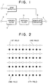
- Fig. 1 is a block diagram showing the typical structure of the conventional motion detection circuit for a MUSE decoder.
- Fig. 2 is a diagram showing the sampling pattern of the luminance signal (Y-signal) for the MUSE (multiple sub-Nyquist sampling encoding) high definition television system.
- the frames of the picture signal are transmitted in cycles of four fields, with a data transmission rate of 16.2 Mbps.
- the sampling points of the first and the second field are represented by white and black circles, respectively.
- the sampling points of the third and the fourth field are represented by white and black diamonds, respectively.
- the edge detector circuit 3 detects the edge component (i.e., the components of high horizontal or vertical frequencies) or the high level component of the signal input to the present data input terminal 1.
- the edge detector circuit 3 converts the information into a signal at a data transmission rate twice as high as that of the input, i.e., to 32.4 Mbps, and supplies the output to the sensitivity converter circuit 6.
- interframe interpolation data input terminal 2 To the interframe interpolation data input terminal 2 is input the interframe interpolation data which consists of the present data (currently transmitted data) and the preceding frame data (the data that has been transmitted one frame earlier), wherein the preceding frame data are interpolated between the present data, such that the data transmission rate of the interframe interpolation data supplied to the interframe interpolation data input terminal 2 is at 32.4 Mbps.
- the MUSE signal includes folding disturbance component (folding noise components) in the horizontal frequency region above 4 MHz (designated by ⁇ 0 ) for processing the still picture image.
- the horizontal filter 4 obtains the one interframe differential from the signal supplied to the interframe interpolation data input terminal 2, and limits the band width of the differential data to the frequency components under ⁇ 0 .
- the MUSE signal includes folding disturbance components (folding noise components) for the moving picture image processing procedure in the vertical frequency region in the neighborhood of 1125/4 (c/h), which is designated by ⁇ 0 .
- the vertical filter 5 removes these disturbance components.
- the output signal of the vertical filter 5 at the data transmission rate 32.4 Mbps is a one interframe differential data from which the folding disturbance components are removed.
- the output signal of the vertical filter 5 represents the motion information of the picture.
- the sensitivity thereof at the edge or the high level components is too high.
- the sensitivity converter circuit 6 thus divides the output signal of the vertical filter 5 representing the motion information by the output signal of the edge detector circuit 3 representing the information on the edge and the high level components, and thereby normalizes the sensitivity of the output signal of the vertical filter 5.
- the motion information data with normalized sensitivity and at the data transmission rate of 32.4 Mbps is obtained at the motion detection data output terminal 7 supplied from the sensitivity converter circuit 6.
- the above conventional motion detection circuit has the disadvantage that the motion information contained in components of horizontal frequency above ⁇ 0 cannot be obtained.
- a further disadvantage is that the edges of the motion detection data are blurred and become unclear.
- EP-A-0 310 032 describes a motion detection circuit which can be used for encoding and decoding a signal in a MUSE system.
- the motion detection circuit is constructed so that an interframe difference signal is passed through a horizontal direction low pass filter and a vertical direction low pass filter which are cascaded, and the interframe difference signal is divided by value obtained by mixing an edge signal of an image and an image level signal of the image. This provides a motion signal.
- EP-A-0 204 450 describes a bandwidth compressed transmission system, applied in relation to a MUSE transmitter and receiver. During decoding, an interframe difference of the transmission signal is detected to obtain a motion detection signal.
- a motion detection circuit for a MUSE decoder for reproducing a high definition television picture signal from a MUSE signal comprising:
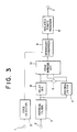
- Fig. 3 is a block diagram showing the structure of a motion detection circuit according to an embodiment of this invention.
- the parts 1 through 3 are similar to those of Fig. 1.
- the edge detector circuit 3 coupled to the present data input terminal 1 supplies its output to the sensitivity converter circuit 6.
- the vertical filter 5 coupled to the interframe interpolation data input terminal 2 supplies its output to the horizontal filter 4 and the delay circuit 8.
- a subtractor 9 receives outputs from the horizontal filter 4 and the delay circuit 8 and calculates the difference therebetween.
- An edge improver circuit 10 receives outputs from the horizontal filter 4, the delay circuit 8 and the subtractor 9, and supplies its output to the sensitivity converter circuit 6.
- the isolated points remover circuit 11 receives the output from the sensitivity converter circuit 6 and supplies its output to the motion detection data output terminal 7.
- the vertical filter 5 obtains the one interframe differential from the interframe interpolation data at 32.4 Mbps received at the interframe interpolation data input terminal 2, and then removes the folding disturbance components near the vertical frequency ⁇ 0 therefrom.
- the output signal at 32.4 Mbps from the vertical filter 5 is input to the delay circuit 8 and the horizontal filter 4.
- the horizontal filter 4 limits the frequency of the input signal under the horizontal frequency ⁇ 0 .
- the delay circuit 8 imparts the same delay to the input signal as the horizontal filter 4.
- the subtractor 9 calculates the difference between the horizontal filter 4 and the delay circuit 8.
- the edge improver circuit 10 improves the edge of the output signal of the horizontal filter 4 on the basis of the outputs of the delay circuit 8 and the subtractor 9.
- Fig. 4 shows the details of the edge improver circuit of Fig. 3.
- the output signal of the subtractor 9 is the difference between the outputs of the delay circuit 8 and the horizontal filter 4, which thus represents the one interframe differential data consisting of components above horizontal frequency ⁇ 0 .
- This signal contains folding disturbance components for the still picture processing.
- a first area filter 12 determines the valid and invalid regions of the output signal of the subtractor 9 on the basis of the output of the horizontal filter 4. Namely, in the regions where the output of the horizontal filter 4 is in the neighborhood of 0 (zero), the first area filter 12 judges that the output of the subtractor 9 is invalid and clips the output signal of the subtractor 9 to 0 (zero) even when the output signal of the subtractor 9 is in a significant region. Then, the output signal of the first area filter 12 vanishes. Otherwise, the output signal of the first area filter 12 is equal to the output signal of the subtractor 9.
- a first peak detector 13 detects maximal or peak values of the output signal of the horizontal filter 4 by comparing the neighboring data values of the output signal of the horizontal filter 4, and outputs pulses corresponding thereto to a horizontal width extender 16 and a judgment circuit 17.
- the horizontal width extender 16 holds all the peak value detection pulses supplied from the first peak detector 13 during the filter tap length of the horizontal filter 4, and, on the basis of the detection pulses thus held therein, selects and outputs the peak value nearest to the current output signal of the horizontal filter 4.
- a ROM circuit 18 effects non-linear conversion to the output signal of the horizontal filter 4 and thereby effects adjustments for the attenuation of the high frequency components.
- a second peak detector 14 detects the peak values of the first area filter 12 by comparing the neighboring data values of the output signal of the first area filter 12. The second peak detector 14 outputs detection pulses corresponding to the detected peaks.
- a comparator 15 compares the levels of the outputs of the horizontal filter 4 and the first area filter 12, outputs high and low level signals indicating the result of comparison. The output signals from the second peak detector 14 and the comparator 15 are supplied to the judgment circuit 17.
- the judgment circuit 17 determines which signal is to be selected from among the outputs of the horizontal filter 4, the horizontal width extender 16 and the ROM circuit 18, and outputs the selection signal indicating the result of selection to the selector 20. Next, the method of judgment of the judgment circuit 17 is described.
- the selector 20 selects from among the outputs of the horizontal filter 4, the horizontal width extender 16, and the ROM circuit 18.
- the second area filter 19 determines the regions of the output of the selector 20 which are blunted near the edge portions, and improves the rise and fall characteristics of the output signal of the selector 20 by means of the output signal of the delay circuit 8. Namely, in the region where the level of the output signal of the delay circuit 8 representing the one interframe differential data from which the folding disturbance components for the moving picture processing is removed is less than the level of the output signal of the selector 20, the second area filter 19 selects as its own output the output signal of the delay circuit 8, disregarding the output signal of the selector 20. In other regions, the second area filter 19 selects as its output the output signal of the selector 20.
- the output of the second area filter 19 constituting the output signal of the edge improver circuit 10 represents the output signal of the horizontal filter 4 the edges of which, however, are improved by means of the circuits interposed therebetween.
- the sensitivity of this output signal of the edge improver circuit 10 at the data transmission rate of 32.4 Mbps is normalized by the sensitivity converter circuit 6.
- the method of operation of the sensitivity converter circuit 6 is the same as in the conventional device of Fig. 1.
- the output signal of the sensitivity converter circuit 6 exhibits improved edges and thus inevitably contains noise components.
- the isolated points remover circuit 11 effects the horizontal and vertical correlation judgement, and removes the noise components from the output signal of the sensitivity converter circuit 6.
- the motion detection data output terminal 7 coupled to the output terminal of the isolated points remover circuit 11 is obtained the motion information data at the data transmission rate of 32.4 Mbps, the sensitivity of which is normalized and the edges thereof are improved.
Landscapes
- Engineering & Computer Science (AREA)
- Multimedia (AREA)
- Signal Processing (AREA)
- Television Systems (AREA)
Description
Claims (1)
- A motion detection circuit for a MUSE decoder for reproducing a high definition television picture signal from a MUSE signal, the circuit comprising:vertical filter means (5) for obtaining a one-interframe differential signal from an interframe interpolation signal consisting of present field transmitted data and data transmitted one frame earlier interpolated therein, said vertical filter means (5) attenuating frequency components in the neighborhood of a vertical frequency of 1125/4 c/h;horizontal filter means (4) for separating an output signal of said vertical filter means (5) into a high frequency component signal above a predetermined horizontal frequency and a low frequency component signal below said predetermined horizontal frequency;edge detector circuit means (3) for extracting edge components of transmitted data of present field from a present data input signal; andsensitivity converter circuit means (6) coupled to said edge detector circuit means (3),characterised in that said motion detection circuit further comprises:first peak detector means (13) coupled to said horizontal filter means (4) for obtaining and outputting a peak value of said low frequency component signal below said predetermined horizontal frequency;horizontal width extender means (16), coupled to said first peak detector means (13) and said horizontal filter means (4), for holding said peak value output from said first peak detector means (13) for a tap length of said horizontal filter means (4), said horizontal width extender means (16) outputting a peak value nearest to a current level of said low frequency component signal below said predetermined horizontal frequency;non-linear circuit means (18) coupled to said horizontal filter means (4), for effecting a non-linear conversion to said low frequency component signal below said predetermined horizontal frequency, thereby effecting an adjustment for an attenuation of high frequency components in said low frequency component signal;first area filter means (12) coupled to said horizontal filter means (4), for determining valid and invalid regions of said high frequency component signal above said predetermined horizontal frequency, said first area filter means (12) clipping said high frequency component signal above said predetermined horizontal frequency in response to a level of said low frequency component signal below said predetermined horizontal frequency;second peak detector means (14) coupled to said first area filter means (12), for obtaining and outputting a peak value of an output signal of said first area filter means (12);comparator means (15) coupled to said horizontal filter means (4) and said first area filter means (12), for comparing levels of said output signal of said first area filter means (12) and said low frequency component signal below said predetermined horizontal frequency;judgement/selector means (17, 20) coupled to said first peak detector means (13), said second peak detector means (14), said horizontal filter means (4), said comparator means (15), said horizontal width extender means (16), and said non-linear circuit means (18), said judgement/selector means (17, 20) selecting one signal from:said low frequency component signal below said predetermined horizontal frequency outputted from said horizontal filter means (4), and output signals of said horizontal width extender means (16) and said non-linear circuit means (18) on the basis of correlation among output signals of said first peak detector means (13), said second peak detector means (14), and said comparator means (15);second area filter means (19) coupled to said vertical filter means (5) and said judgement/ selector means (17, 20), for selecting one from output signals of said vertical filter means (5) and said judgement/selector means (17, 20) in response to a level of the output signal of said vertical filter means (5); andisolated points remover circuit means (11) coupled to said sensitivity converter circuit means (6), for removing noise components having no correlation with neighbouring data from an output signal of said sensitivity converter circuit means (6) on the basis of a horizontal and vertical correlation judgement,said sensitivity converter circuit means (6) being coupled to said second area filter means (19), for effecting non-linear conversion to an output signal of said second area filter by means of an output signal of said edge detector circuit means (3) thereby normalizing a sensitivity of said output signal of said second area filter means (19).
Applications Claiming Priority (8)
| Application Number | Priority Date | Filing Date | Title |
|---|---|---|---|
| JP283419/91 | 1991-10-30 | ||
| JP28341991A JP2643043B2 (en) | 1991-10-30 | 1991-10-30 | Motion detection circuit |
| JP79565/92 | 1992-04-01 | ||
| JP7956592 | 1992-04-01 | ||
| JP130580/92 | 1992-05-22 | ||
| JP13058092 | 1992-05-22 | ||
| JP13058292 | 1992-05-22 | ||
| JP130582/92 | 1992-05-22 |
Publications (3)
| Publication Number | Publication Date |
|---|---|
| EP0540347A2 EP0540347A2 (en) | 1993-05-05 |
| EP0540347A3 EP0540347A3 (en) | 1994-06-08 |
| EP0540347B1 true EP0540347B1 (en) | 1999-01-13 |
Family
ID=27466325
Family Applications (1)
| Application Number | Title | Priority Date | Filing Date |
|---|---|---|---|
| EP92309955A Expired - Lifetime EP0540347B1 (en) | 1991-10-30 | 1992-10-30 | Motion detection circuit for high definition television picture signal based on the muse system |
Country Status (3)
| Country | Link |
|---|---|
| US (1) | US5497203A (en) |
| EP (1) | EP0540347B1 (en) |
| DE (1) | DE69228167T2 (en) |
Families Citing this family (11)
| Publication number | Priority date | Publication date | Assignee | Title |
|---|---|---|---|---|
| EP1538843A3 (en) * | 1994-04-20 | 2006-06-07 | Oki Electric Industry Company, Limited | Image Encoding and Decoding Method and Apparatus Using Edge Synthesis and Inverse Wavelet Transform |
| JP3228638B2 (en) * | 1994-06-08 | 2001-11-12 | 松下電器産業株式会社 | Moving object detection method using background difference method |
| KR970010094B1 (en) * | 1994-06-24 | 1997-06-21 | Korea Telecommunication | Improved motion vector extraction method |
| US5991463A (en) * | 1995-11-08 | 1999-11-23 | Genesis Microchip Inc. | Source data interpolation method and apparatus |
| KR100472545B1 (en) * | 1997-12-20 | 2005-05-16 | 주식회사 대우일렉트로닉스 | Vertex coding apparatus employing the length of two codewords |
| JP4193233B2 (en) * | 1998-08-12 | 2008-12-10 | ソニー株式会社 | Motion determination device, method and image information conversion device |
| JP2000078580A (en) * | 1998-08-28 | 2000-03-14 | Sony Corp | Apparatus and method for detecting motion vector, and provided medium |
| JP3285545B2 (en) * | 1998-09-29 | 2002-05-27 | 松下電器産業株式会社 | Motion detection circuit and noise reduction device |
| JP3340976B2 (en) * | 1999-06-21 | 2002-11-05 | 松下電器産業株式会社 | Motion detection circuit and noise reduction device |
| JP4508279B2 (en) * | 2008-07-17 | 2010-07-21 | ソニー株式会社 | Image processing apparatus, image processing method, and program |
| US9420873B2 (en) * | 2011-10-11 | 2016-08-23 | Jaimie David Gordon | Flash vortex brush device and method |
Family Cites Families (14)
| Publication number | Priority date | Publication date | Assignee | Title |
|---|---|---|---|---|
| US4692801A (en) * | 1985-05-20 | 1987-09-08 | Nippon Hoso Kyokai | Bandwidth compressed transmission system |
| JPS6386990A (en) * | 1986-09-30 | 1988-04-18 | Nippon Hoso Kyokai <Nhk> | Move detection method |
| JPH0191586A (en) * | 1987-10-02 | 1989-04-11 | Nippon Hoso Kyokai <Nhk> | Moving detection circuit |
| JP2706495B2 (en) * | 1988-11-22 | 1998-01-28 | 松下電器産業株式会社 | Image signal processing device |
| US4953032A (en) * | 1988-11-30 | 1990-08-28 | Hitachi, Ltd. | Motion signal generating circuit for use in a television receiver |
| JP2576612B2 (en) * | 1988-12-28 | 1997-01-29 | 日本ビクター株式会社 | Signal converter |
| JPH0683435B2 (en) * | 1989-02-03 | 1994-10-19 | 三洋電機株式会社 | Subsample video signal demodulator |
| US4982288A (en) * | 1989-02-16 | 1991-01-01 | Matsushita Electric Industrial Co., Ltd. | High definition television receiver enabling picture-in picture display |
| JPH03108976A (en) * | 1989-09-22 | 1991-05-09 | Fujitsu General Ltd | MUSE decoder |
| US5027201A (en) * | 1989-12-21 | 1991-06-25 | Rca Licensing Corporation | Motion detection apparatus as for an interlace to non-interlace scan converter |
| EP0460928A3 (en) * | 1990-06-07 | 1993-09-01 | Matsushita Electric Industrial Co., Ltd. | Video signal converting apparatus |
| US5166788A (en) * | 1990-06-29 | 1992-11-24 | Samsung Electronics Co., Ltd. | Motion signal processor |
| JP2538432B2 (en) * | 1991-03-15 | 1996-09-25 | 三洋電機株式会社 | Motion detection circuit |
| JPH04286484A (en) * | 1991-03-15 | 1992-10-12 | Sanyo Electric Co Ltd | Motion detecting circuit |
-
1992
- 1992-10-29 US US07/968,532 patent/US5497203A/en not_active Expired - Fee Related
- 1992-10-30 EP EP92309955A patent/EP0540347B1/en not_active Expired - Lifetime
- 1992-10-30 DE DE69228167T patent/DE69228167T2/en not_active Expired - Fee Related
Also Published As
| Publication number | Publication date |
|---|---|
| EP0540347A3 (en) | 1994-06-08 |
| DE69228167T2 (en) | 1999-07-22 |
| US5497203A (en) | 1996-03-05 |
| DE69228167D1 (en) | 1999-02-25 |
| EP0540347A2 (en) | 1993-05-05 |
Similar Documents
| Publication | Publication Date | Title |
|---|---|---|
| EP0629083B1 (en) | Interlaced-to-progressive scanning converter having a double-smoothing function and a method therefor | |
| KR960004130B1 (en) | Noise Reduction Circuit of Video Signal | |
| JP3331138B2 (en) | Luminance / color signal separation device for composite video signal | |
| EP0592196B1 (en) | Noise eliminating circuits | |
| US4754322A (en) | YC-signal separation circuit responsive to magnitude of vertical correlation | |
| EP0731601B2 (en) | Video signal noise reduction apparatus | |
| US6904096B2 (en) | Video data processing device and video data processing method | |
| JP3488195B2 (en) | Noise value determination method, noise value determination circuit, and television receiver | |
| JPS61501672A (en) | Television signal processing device with movement detector | |
| US5381183A (en) | Motion-adaptive scanning-line conversion circuit | |
| US5155582A (en) | Dot crawling interference elimination device and color subcarrier vertical correlation detection device | |
| US5497203A (en) | Motion detection circuit for high definition television based on muse | |
| US5093715A (en) | Adaptive comb filter for separating at least one component of a video signal | |
| EP0540102A1 (en) | Arrangement for reducing artifacts in video signals | |
| Ishizu et al. | Digital signal processing for improved NTSC television receiver | |
| EP0444329A1 (en) | Improved image edge direction detection apparatus in video systems | |
| JP2784806B2 (en) | Motion area detection circuit | |
| JP2989362B2 (en) | Motion detection circuit and motion detection method | |
| JP2727611B2 (en) | Filter control circuit | |
| JP2643043B2 (en) | Motion detection circuit | |
| JP4368036B2 (en) | Video signal processing circuit | |
| JP2928597B2 (en) | Receiver for band-compressed television signal | |
| JP3028880B2 (en) | High definition television receiver | |
| JPH05145802A (en) | Impulse noise elimination device | |
| JP2685542B2 (en) | Chroma signal processing circuit |
Legal Events
| Date | Code | Title | Description |
|---|---|---|---|
| PUAI | Public reference made under article 153(3) epc to a published international application that has entered the european phase |
Free format text: ORIGINAL CODE: 0009012 |
|
| AK | Designated contracting states |
Kind code of ref document: A2 Designated state(s): DE GB |
|
| PUAL | Search report despatched |
Free format text: ORIGINAL CODE: 0009013 |
|
| AK | Designated contracting states |
Kind code of ref document: A3 Designated state(s): DE GB |
|
| 17P | Request for examination filed |
Effective date: 19940621 |
|
| 17Q | First examination report despatched |
Effective date: 19960723 |
|
| GRAG | Despatch of communication of intention to grant |
Free format text: ORIGINAL CODE: EPIDOS AGRA |
|
| GRAG | Despatch of communication of intention to grant |
Free format text: ORIGINAL CODE: EPIDOS AGRA |
|
| GRAH | Despatch of communication of intention to grant a patent |
Free format text: ORIGINAL CODE: EPIDOS IGRA |
|
| GRAH | Despatch of communication of intention to grant a patent |
Free format text: ORIGINAL CODE: EPIDOS IGRA |
|
| GRAA | (expected) grant |
Free format text: ORIGINAL CODE: 0009210 |
|
| AK | Designated contracting states |
Kind code of ref document: B1 Designated state(s): DE GB |
|
| REF | Corresponds to: |
Ref document number: 69228167 Country of ref document: DE Date of ref document: 19990225 |
|
| PLBE | No opposition filed within time limit |
Free format text: ORIGINAL CODE: 0009261 |
|
| 26N | No opposition filed | ||
| REG | Reference to a national code |
Ref country code: GB Ref legal event code: IF02 |
|
| PGFP | Annual fee paid to national office [announced via postgrant information from national office to epo] |
Ref country code: GB Payment date: 20021030 Year of fee payment: 11 |
|
| PGFP | Annual fee paid to national office [announced via postgrant information from national office to epo] |
Ref country code: DE Payment date: 20021031 Year of fee payment: 11 |
|
| PG25 | Lapsed in a contracting state [announced via postgrant information from national office to epo] |
Ref country code: GB Free format text: LAPSE BECAUSE OF NON-PAYMENT OF DUE FEES Effective date: 20031030 |
|
| PG25 | Lapsed in a contracting state [announced via postgrant information from national office to epo] |
Ref country code: DE Free format text: LAPSE BECAUSE OF NON-PAYMENT OF DUE FEES Effective date: 20040501 |
|
| GBPC | Gb: european patent ceased through non-payment of renewal fee |
Effective date: 20031030 |