EP0540221A1 - Image forming apparatus - Google Patents
Image forming apparatus Download PDFInfo
- Publication number
- EP0540221A1 EP0540221A1 EP92309526A EP92309526A EP0540221A1 EP 0540221 A1 EP0540221 A1 EP 0540221A1 EP 92309526 A EP92309526 A EP 92309526A EP 92309526 A EP92309526 A EP 92309526A EP 0540221 A1 EP0540221 A1 EP 0540221A1
- Authority
- EP
- European Patent Office
- Prior art keywords
- image
- circuit
- reference wave
- density data
- density
- Prior art date
- Legal status (The legal status is an assumption and is not a legal conclusion. Google has not performed a legal analysis and makes no representation as to the accuracy of the status listed.)
- Granted
Links
Images


Classifications
-
- H—ELECTRICITY
- H04—ELECTRIC COMMUNICATION TECHNIQUE
- H04N—PICTORIAL COMMUNICATION, e.g. TELEVISION
- H04N1/00—Scanning, transmission or reproduction of documents or the like, e.g. facsimile transmission; Details thereof
- H04N1/46—Colour picture communication systems
- H04N1/52—Circuits or arrangements for halftone screening
-
- H—ELECTRICITY
- H04—ELECTRIC COMMUNICATION TECHNIQUE
- H04N—PICTORIAL COMMUNICATION, e.g. TELEVISION
- H04N1/00—Scanning, transmission or reproduction of documents or the like, e.g. facsimile transmission; Details thereof
- H04N1/40—Picture signal circuits
- H04N1/405—Halftoning, i.e. converting the picture signal of a continuous-tone original into a corresponding signal showing only two levels
- H04N1/4055—Halftoning, i.e. converting the picture signal of a continuous-tone original into a corresponding signal showing only two levels producing a clustered dots or a size modulated halftone pattern
- H04N1/4056—Halftoning, i.e. converting the picture signal of a continuous-tone original into a corresponding signal showing only two levels producing a clustered dots or a size modulated halftone pattern the pattern varying in one dimension only, e.g. dash length, pulse width modulation [PWM]
-
- H—ELECTRICITY
- H04—ELECTRIC COMMUNICATION TECHNIQUE
- H04N—PICTORIAL COMMUNICATION, e.g. TELEVISION
- H04N1/00—Scanning, transmission or reproduction of documents or the like, e.g. facsimile transmission; Details thereof
- H04N1/46—Colour picture communication systems
- H04N1/56—Processing of colour picture signals
- H04N1/58—Edge or detail enhancement; Noise or error suppression, e.g. colour misregistration correction
Definitions
- the present invention relates to a color image forming apparatus in which: one matrix pixel image data is divided into small pixels m x n (the width x the length) considering the adjoining pixel data, and after that, the center of gravity of each line is found; the phase of the reference wave is deviated according to the center of gravity; and dot recording composed of n small scanning lines is conducted by the modulated signal of the pixel density data modulated by the reference wave signal so that a character and a halftone image can be reproduced.
- the recording apparatus of the present invention is used for a printing apparatus or a displaying apparatus.
- a digital halftone image is reproduced in the following manner: an original image is read by a scanner to get on image signal; and image density data in which the image signal is gradation-corrected, A/D converted, and shading-corrected, is modulated by a reference signal and thus digital image is obtained.
- the invention relates to an image forming apparatus wherein dot-recording is made for reproduction of characters and halftone images by a laser diode oscillated by modulation signals in which density data are modulated by reference signals.
- an object of the present invention is to provide an image forming apparatus in which resolution of the image, which is formed from scanner data, C.G data, font data, or the like, is improved, and high quality images having no longitudinal streaks are recorded.
- an image forming apparatus of the invention capable of conducting high density pixel recording with density data of small pixels in an objective pixel determined based on density data of pixels adjoining the objective pixel
- the objective pixel determines a recording position for each color based on density distribution of the adjoining pixels when the recording position of each color is modulated in the primary scanning direction and secondary scanning direction based on density distribution of both the objective pixel and the adjoining pixels.
- preferable resolution and gradation matching an image can be realized by making the cycle of a reference wave to be variable corresponding to the image.
- an image forming apparatus of the invention there are provided a means for image judgment on the objective pixel mentioned above and a means which modulates a recording position using a reference wave with a long cycle when an image is judged to be a halftone area under the image judgment, and modulates the recording position using a reference wave with a short cycle when an image is judged to be a character area.
- an image forming apparatus of the invention a plurality of scanning operations are conducted for a unit pixel and an image is formed with a scanning position deviated by a selectable reference wave for a character reproduction area and with a scanning width changed by a selectable reference wave for a halftone reproduction area.
- the aforementioned image forming apparatus wherein a plurality of pixels are used and a phase of a reference wave differs for each color is a preferable embodiment.
- Fig. 1 is a block diagram of an image processing circuit in the first example of an image forming apparatus of the invention
- Fig. 2 is a block diagram showing an example of a determination circuit for a reference wave phase in the circuit shown in Fig. 1
- Fig. 3 is a block diagram showing an example of a modulation circuit in the circuit shown in Fig. 1.
- Fig. 4 is a perspective view showing the general constitution of an image forming apparatus of the invention.
- Fig. 5 a diagram illustrating the RE process used for a determination of a reference wave phase
- Fig. 5 a diagram illustrating the RE process used for a determination of a reference wave phase
- FIG. 7 is a diagram showing an example wherein an objective pixel for the RE process is divided into the number of 2x2, and Fig. 8 is another example showing the same occasion as in Fig. 7.
- Fig. 9 is a diagram for illustrating the phase displacement for a reference wave in the case of a character area.
- Fig. 10 is a time chart showing each signal in the case of a character area for a modulation signal generation circuit in the example shown in Fig. 1.
- Fig. 11 is a diagram for illustrating the phase displacement for a reference wave in the case of a halftone area.
- Fig. 12 is a time chart showing each signal in the case of a halftone area for a modulation signal generation circuit in the example shown in Fig. 1.
- FIG. 13 is a graph showing the characteristics of a high ⁇ photoreceptor used in the present example
- Fig. 14 is a cross-sectional view showing the concrete example of constitution for the high ⁇ photoreceptor used in the present example.
- Fig. 15 is a diagram showing a semiconductor laser alley in the example shown in Fig. 4, and
- Fig. 16 is a diagram showing a scanning locus of a laser spot by means of a semiconductor laser alley shown in Fig. 13.
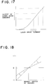
- Fig. 17 is a graph showing an example of the relation between driving current for a semiconductor laser and laser radiation output.
- Fig. 18 is a graph showing an example of an occasion wherein the relation between a center of gravity in the primary scanning direction of a small scanning line and a recording position is changed.
- Fig. 15 is a diagram showing a semiconductor laser alley in the example shown in Fig. 4
- Fig. 16 is a diagram showing a scanning locus of a laser spot by means of a semiconductor laser alley shown
- FIG. 19 is a graph showing an example of an occasion wherein average density in the secondary scanning direction of a small scanning line is converted.
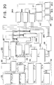
- Fig. 20 is a block diagram showing an image processing circuit in the second example of the invention, and
- Fig. 21 is a block diagram showing a phase determination circuit for a reference wave in Fig. 20.
- Fig. 22 is a block diagram showing a modulation signal generation circuit in the third example, and
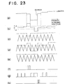
- Fig. 23 is a time chart showing each signal in the case of a character reproduction area for a modulation signal generation circuit in the third example.
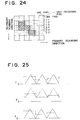
- Fig. 24 is an illustrative diagram wherein a latent image in a character reproduction area is formed by modulation signals in the third example.
- Fig. 20 is a block diagram showing an image processing circuit in the second example of the invention
- Fig. 21 is a block diagram showing a phase determination circuit for a reference wave in Fig. 20.
- Fig. 22 is a block diagram showing a modulation signal generation circuit in
- Fig. 25 is a diagram showing an example of a triangular wave which is a reference wave of a halftone reproduction area in the third example
- Fig. 26 is an illustrative diagram wherein a latent image in a halftone reproduction area is formed by modulation signals in the third example
- Fig. 27 is a diagram showing a reference wave used in the fourth example of the invention
- Fig. 28 is a diagram showing an electrostatic latent image in the fourth example of the invention
- Fig. 29 is a diagram showing an electrostatic latent image in the fifth example of the invention.
- Fig. 4 is a perspective view showing general constitution of the image forming apparatus in the present example.
- a color image can be obtained by the image forming apparatus 400 as follows: After a photoreceptor has been uniformly charged, a dot-shaped electrostatic latent image is formed thereon by a spot light which has been pulse-modulated in accordance with a modulation signal obtained through differential amplification between an analog image density signal which can be obtained by D/A-converting a digital image density signal sent from a computer or a scanner, and a reference signal, and this electrostatic latent image is reversely developed by toner so that a dotshaped toner image is formed.
- the aforementioned charging, exposing and developing processes are repeatedly conducted so that a color toner image can be formed on the surface of a photoreceptor, and then the obtained color toner image is transferred, separated and fixed.
- the image forming apparatus 400 is composed of, a drum-shaped photoreceptor 401 (hereinafter, referred to as a photoreceptor) which is rotated in the direction of an arrow, a scorotron charger 402 which gives a uniform electric charge on the aforementioned photoreceptor 401, an optical scanning system 430, developing units 441 - 444 which are loaded with yellow, magenta, cyan and black toners, a scorotron transfer unit 462, a separator 463, a fixing roller 464, a cleaning unit 470, and a discharger 474.
- a drum-shaped photoreceptor 401 hereinafter, referred to as a photoreceptor
- a scorotron charger 402 which gives a uniform electric charge on the aforementioned photoreceptor 401
- an optical scanning system 430 developing units 441 - 444 which are loaded with yellow, magenta, cyan and black toners
- a scorotron transfer unit 462 a separator 463,
- Fig. 14 is a diagram showing an example of a specific structure of a high ⁇ photoreceptor 401 used in the present example.
- the photoreceptor 401 is composed of a conductive support 401A, an intermediate layer 401B, and a photosensitive layer 401C.
- the thickness of the photosensitive layer 401C is 5 - 100 ⁇ m, and preferably 10 - 50 ⁇ m.
- the photoreceptor 401 is made of an aluminum drum-shaped conductive support 401A.
- On the aforementioned support 401A is formed the intermediate layer 401B of 0.1 ⁇ m in thickness, which is made from ethylene-vinyl acetate, and on the intermediate layer 401B is provided the photosensitive layer 401C, the thickness of which is 35 ⁇ m.
- a drum of 150 mm in diameter which is made from aluminum, steel or copper is used for the conductive support 401A.
- a belt-shaped conductive support is also used which is made in such a manner that a metallic layer:is vapor-deposited or laminated on a paper or a plastic film.
- a metallic belt made from nickel by means of electroforming may be also used.
- the intermediate layer 401B can endure a high potential charging of ⁇ 500 - ⁇ 2000V as a photoreceptor, and it is further preferable that the intermediate layer 401B is provided with a hall mobility so that the flow of electrons from the conductive support 401C can be prevented when it has been charged positive, and so that an excellent light decay characteristic can be obtained due to the avalanche effect. Therefore, it is preferable that a positive charging type of electric charge conveyance material which has been disclosed in Japanese Patent Application 188975/1986 by the inventors, is added to the intermediate layer 401B by not more than 10 weight percent.
- the photosensitive layer 401C is formed by coating a coating agent on an intermediate layer and after that the coated layer is dried and heat-treated if necessary, wherein the coating agent is prepared as follows: basically, electric charge conveyance material is not added into the photosensitive layer 401C; phthalocyanine fine particles of 0.1 - 1 ⁇ m in diameter composed of a photoconductive pigment, an antioxidant and a binder resin are mixed and dispersed in a solvent.
- a photosensitive layer is composed as follows: a photoconductive material composed of a phtoconductive pigment and a small amount of electric charge conveyance material, the amount of which is not more than 1/5 of the aforementioned photoconductive pigment, or preferably 1/1000 - 1/10 (weight percent) of the pigment, and an antioxidant are dispersed in a binder resin.
- a photoconductive material composed of a phtoconductive pigment and a small amount of electric charge conveyance material, the amount of which is not more than 1/5 of the aforementioned photoconductive pigment, or preferably 1/1000 - 1/10 (weight percent) of the pigment, and an antioxidant are dispersed in a binder resin.
- color toner images are superimposed on a photoreceptor. Accordingly, a photoreceptor, the spectral sensitivity of which is on the infrared side, and a semiconductor laser of infrared light are used so that the beam sent from the optical scanning system can not shade the color toner image.
- the light decay characteristic of the high ⁇ photoreceptor of the present invention will be explained as follows.
- Fig. 13 is a graph showing the outline of a high ⁇ photoreceptor.
- V1 is a charging potential (V)
- V0 is an initial potential (V) before exposure
- L1 is the amount ( ⁇ J/cm2) of light of the illuminated laser beam which is required to reduce initial potential V0 to 4/5
- L2 is the amount ( ⁇ J/cm2) of light of the illuminated laser beam which is required to reduce initial potential V0 to 1/5.
- a preferable range of L2/L1 is 1.0 ⁇ L2/L1 ⁇ 1.5.
- the photoreceptor potential of the exposure section is 10V.
- the absolute value of the differential coefficient of the potential characteristic is decayed a little when the amount of light is small, and decayed sharply as the amount of light is increased as shown in Fig. 13.
- the sensitivity characteristic is bad for a certain period of time L1.
- the light sensitivity is highly increased so that the light decay curve goes downward almost linearly, in other words, the photoreceptor shows a super-high ⁇ characteristic. It can be considered that the photoreceptor 401 acquires a high ⁇ characteristic using an avalanche phenomenon under a high charging potential of +500 - +200V.
- an objective matrix pixel of the image density data is composed of small pixels m ⁇ n (width ⁇ length), and a distribution of the density data of adjoining pixels including the objective pixel, is replaced with the distribution of small pixels m x n in one pixel, and the image is formed by the following method: a position in which dots of n rows are written is displaced when a phase of a reference wave in each row of small pixels is displaced according to image density data of small pixels obtained by distributing data of the objective pixel multiplied by constant P corresponding to the distribution. Displacement of the position in which dots are written will be referred to as recording position modulation, hereinafter.
- processing to convert the image density data of the objective pixel into the image density data of small pixels obtained by dividing the objective pixel into m ⁇ n will be referred to as resolution enhancing processing (RE processing), hereinafter. Due to RE processing, high density recording can be conducted. In this case, a high ⁇ photoreceptor is specifically effective in order to form a latent image corresponding exactly to the reference wave.
- RE processing is conducted when 1 the image density data of the objective pixel is not less than a first threshold value, that is, not less than the specific density, namely the first threshold value.
- a first threshold value that is, not less than the specific density, namely the first threshold value.
- RE processing is not conducted on a background portion of a document, and small pixels m ⁇ n are set to have a uniform density. In the case of CRT, this data display can be possible.
- a reference wave whose density center exists in the center of the image density is selected.
- a color image forming apparatus in which high density image recording is conducted according to density distribution data in the objective pixel which is determined corresponding to density data of the pixels adjoining the objective pixel, a color image forming apparatus which is characterized as follows is preferable: when a specific density data of the objective pixel is not less than the first threshold value, recording position modulation is conducted according to the determined density distribution; or when a specific density data of the pixel is not more than the second threshold value recording position modulation is conducted according to the determined density distribution.
- Fig. 5(a) is a plan view in which the adjoining pixels including the objective pixel m5 are expressed as m1 to m9 when the objective pixel is defined as m5, and the objective pixel m5 is divided into 3 ⁇ 3 small pixels.
- Fig. 5(b) is an enlarged view in which each small pixel is expressed by s1 to s9 when the objective pixel is divided into small pixels of 3 ⁇ 3.
- m1 to m9 and s1 to s9 also express the density of each portion.
- a term of (9 ⁇ m5 ⁇ P ⁇ mi/A) expresses a density in which the density of the objective pixel m5 multiplied by P is distributed to each small pixel according to density ratio of the adjoining pixels
- (1-P) ⁇ m5 expresses a density in which the residual density of the objective pixel m5 is distributed equally to each small pixel, so that an element of unsharpness is taken into the equation.
- Fig. 6(a) is an illustration showing an example of the density distribution of the adjoining pixels including the objective pixel m5.
- Fig. 7 and Fig. 8 show an example in which the objective pixel m5 is divided into 2 ⁇ 2 small pixels.
- Fig. 7(a) is an illustration showing an example in which the objective pixel m5 is divided into 2 ⁇ 2 small pixels.
- Fig. 7(b) is an illustration showing an example of the adjoining pixels relating to small pixels s1 to s4 in the objective pixel.
- Density of s1, s2, s3, and s4 is calculated according to Equation 1.
- Fig. 8(a) is an illustration showing another example in which the objective pixel m5 is divided into 2 ⁇ 2 small pixels.
- Fig. 8(b) is an illustration showing another example of the adjoining pixels relating to small pixels s1 to s4 in the objective pixel. Density calculation of s1, s2, s3, and s4 is conducted according to Equation 2.
- Fig. 1 is a block diagram showing an example of an image processing circuit which is used in a color image forming apparatus of the present invention (an example in which the objective pixel is divided into 3 ⁇ 3).
- Fig. 2 is a block diagram showing a circuit for determining a reference wave phase and
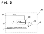
- Fig. 3 is a block diagram showing a modulation circuit in the present example.
- An image processing circuit 1000 of this embodiment is a circuit composing a drive circuit of an optical scanning system.
- the image processing circuit 1000 is composed of an image data processing circuit 100, a modulation signal generating circuit 200, and a raster scanning circuit 300.
- the image data processing circuit 100 is a circuit to interpolate the edge portion of font data and output the obtained data.
- the image data processing circuit 100 is composed of an input circuit 110, font data generating circuit 120, font data storing circuit 130, and interpolation data generating circuit 140.
- a character code signal, size code signal, position code signal, and color code signal are sent from the input circuit 110 to the font data generating circuit 120.
- the font data generating circuit 120 selects an address signal from 4 kinds of input signals and sends the selected signal to the font data storing circuit 130.
- the font data storing circuit 130 sends font data corresponding to the address signal to the font data generating circuit 120.
- the font data generating circuit 120 sends the font data to the interpolation data generating circuit 140.
- the interpolation data generating circuit 140 interpolates a zig-zag and jump of the image density data which are caused on the edge of font data using an intermediate density, and sends the interpolated data to the image density data storing circuit 210 composed of a frame memory. Concerning the color to be generated, the corresponding data is converted to the density data of yellow (Y), magenta (M), cyan (C), and black (BK) in accordance with a color code. In the way described above, the font is bit-map-developed in each frame memory under the condition that the shape is the same and the density ratio of each color is different.
- the modulation signal generator 200 is composed of the image density data memory circuit 210, a read-out circuit 220, a latch circuit 230, an image discrimination circuit 231, an MTF correction circuit 232, a ⁇ correction circuit 233, circuit for determining reference wave phase 240, select circuits 250A to 250C, modulation circuits 260A to 260C, reference clock generator 280, triangular wave generating circuit 290 and delay circuits group 291.
- the image density data storing circuit 210 is usually a page memory (which is referred to as a page memory 210, hereinafter). That is, the image density data storing circuit 210 is a RAM which stores the data by the unit of a page, and at least has a capacity of storing a page of multi-value image density data. When the apparatus is used for a color printer, the apparatus must be provided with a storage capacity enough to store the image density signal corresponding to a plurality of colors, for example, yellow, magenta, cyan and black.
- the read-out circuit 220 reads out continuous image density data of every one scanning line, which is continued in synchronization with the standard clock DCK0 from the image density data memory circuit (page memory) 210, and sends it to the RE processing circuit, the image discrimination circuit 231, and MTF correction circuit 232, wherein an index signal is used as a trigger.
- the latch circuit 230 is a circuit which latches the image density data only when the processing in the circuit for determining reference wave phase 240.
- the reference clock generator 280 is a pulse generating circuit, and generates a pulse signal with a cycle period identical to that of the pixel clock, and sends it to the read-out circuit 220, triangular wave generating circuit 290, developing circuits group 291 and modulation circuits 260A - 260C.
- This clock is called reference clock DCK0 for convenience' sake.
- the numeral 290 represents a triangular wave generation circuit and it forms, based on reference clock DCK0, waveforms for both reference triangular wave ⁇ 0′ which is a reference wave whose cycle is the same as that of a pixel clock and triangular wave ⁇ 0 ⁇ which is a reference wave whose cycle is two times that of a pixel clock.
- a plurality of clocks DCK1′ - DCK4′ and DCK1 ⁇ - DCK4 ⁇ each having a phase difference of a constant period of cycle (1/6 cycles in the present example) against the reference clock DCK0 and the clock whose cycle is two times that of a reference clock are generated, and based upon this, it outputs triangular waves ⁇ 1′ - ⁇ 4′ and ⁇ 1 ⁇ - ⁇ 4 ⁇ (in this example, triangular waves ⁇ 1′ and ⁇ 1 ⁇ whose cycle is ahead by 1/6 cycles, triangular waves ⁇ 2′ and ⁇ 2 ⁇ whose cycle is ahead by 2/6 cycles, triangular waves ⁇ 3′ and ⁇ 3 ⁇ whose cycle is behind by 1/6 cycles and triangular waves ⁇ 4′ and ⁇ 4 ⁇ whose cycle is behind by 2/6 cycles).
- Select circuits 250A - 250C have input portion for triangular waves ⁇ 1′ - ⁇ 4′ and ⁇ 1 ⁇ - ⁇ 4 ⁇ each being different, in terms of phase, from the aforementioned reference triangular waves ⁇ 0′ and ⁇ 0 ⁇ , and one of the aforementioned triangular waves is selected by selection signals coming from reference wave phase determination circuit 240 which will be stated later, and is sent to input terminal T of modulation circuit 260A - 260C.
- the modulation circuits 260A - 260C have the same circuit structure.
- the modulation circuits are provided with the D/A-conversion circuit 261, the comparator 262, and input portion T for the reference triangular wave ⁇ 0′ and triangular waves having phases each being deviated by 1/6 cycles as well as triangular wave ⁇ 0 ⁇ having a double cycle and triangular waves having phases each being deviated by 1/6 cycles.
- the image density data inputted through latch circuit 230 is D/A-converted by the D/A-conversion circuit 261 synchronously with reference clock DCK0, and the modulated image density data are compared with a reference wave that is the trianular wave inputted from select circuits 250A- 250C.
- pulse-width-modulated signals are obtained.
- Image discrimination circuit 231 selects a reference wave from ⁇ 0′ - ⁇ 4′ for a character area and from ⁇ 0 ⁇ - ⁇ 4 ⁇ for a halftone area.
- the circuit for determining reference wave phase 240 is composed of a one line delay circuit 242, a one clock delay circuit 243, and an arithmetic processing circuit 241.
- the one line delay circuit 242 operates as follows: the image density data of the first one scanning line of three scanning lines of the image density data in which one scanning line is sent at a time is delayed by two line scanning time periods by the one line delay circuit 242; the image density data of the second one scanning line is delayed by one line scanning time period by the circuit 242; and the image density data of the last one scanning line is not delayed.
- each image density data is delayed for the time of two reference clocks or one reference clock by the one clock delay circuit 243, and all image density data of the pixels, which include the objective pixel and adjoin the pixel, are sent at the same time to the arithmetic processing circuit 241.
- the image density data of the small pixel is obtained by the RE processing.
- the image density data of the obtained small pixel is divided into a small scanning line including s1, s2, s3 ⁇ shown in Fig. 5, the small scanning line including s4, s5, s6 ⁇ , and the small scanning line including s7, s8, s9 ⁇ , and one scanning line of the original pixel corresponds to these three scanning lines of the small pixels.
- the arithmetic processing circuit 241 calculates average density of each small scanning line and the position of gravity center of the density data in each small scanning line, outputs the average density data to emission output of laser drivers 301A to 301C and outputs different selected signals based on the position data of gravity center to select circuits 250A to 250C from the output terminals OA to OC.
- the position data for selecting triangular wave of gravity center of the second small scanning line which is determined by the position of gravity center of density of s4, s5, and s6 of the pixel m5 is outputted to select circuit 250B
- the position data for selecting triangular wave of gravity center of the third small scanning line which is determined by the position of gravity center of density of s7, s8, and s9 of the pixel m5 is outputted to select circuit 250C.
- Fig. 9 is an illustration showing an example of the relation between the triangular waves having different phases and the objective pixel.
- the arithmetic processing circuit 241 controls an emission output of laser drivers 301A to 301C corresponding to the average density in the pixel m5 of each small scanning line.
- the circuit 241 controls a semiconductor laser 301A to emit the beam in proportion to the average density of s1, s2 and s3.
- Fig. 17 is a graph showing an example of the relation between a driving current of the semiconductor laser and the output of laser emission.
- the density data of the obtained small pixel is divided into a small scanning line including s1, s2, s3 ⁇ , the small scanning line including s4, s5, s6, and the small scanning line including s7, s8, and s9, in m5 and m6 in Fig. 5, and three small scanning lines of the small pixels correspond to one scanning line in every two pixels of the original pixel.
- the arithmetic processing circuit 241 further calculates average density of each small scanning line and a position of gravity center of density data within one original pixel of each scanning line, and outputs the average density data to emission output of laser drivers 301A - 301C and outputs each different selection signal based on the data of the gravity position to select circuits 250A- 250C from output terminals OA - OC.
- the triangular wave selection signals of the second small scanning line which is determined by the position of gravity center of density of s4, s5, and s6 of the pixels m5 and m6 is outputted to the select circuit 250B
- the triangular wave selection signals of the third small scanning line which is determined by the position of gravity center of density of s7, s8, and s9 of the pixels m5 and m6, is outputted to the select circuit 250C.
- Fig. 11 is an illustration showing an example of the relation between the triangular waves having the aforesaid different phase and the objective pixel mentioned above.
- the arithmetic processing circuit 241 controls emission output of laser drivers 301A to 301C, depending on the average density in pixels m5 and m6 of each small scanning line.
- the circuit 241 controls the semiconductor laser 301A to emit the laser beam in proportion to the average density of s1, s2, and s3 between each pixel.
- Fig. 17 is a graph showing an example of the relation between a driving current of a semiconductor laser and an output of the laser emission.
- the image discrimination circuit 231 discriminates the image data whether they are the first threshold value or the second one, and when it discriminates to be the area other than the first and second threshold values, selection signals which do not output a triangular wave in which reference wave phase determining circuit 240 has selected all color components but output reference triangular waves ⁇ 0′ and ⁇ 0 ⁇ are sent to select circuits 250A - 250C, and MTF correction circuit 232 is not caaused to operate. Due to the aforementioned, the image density data other than what is read out from the read-out circuit 220 is not corrected by the MTF correction circuit 232, and after it has been corrected by the ⁇ correction circuit 233, it is sent to modulation circuits 260A to 260C through the latch circuit 230.
- the image discrimination circuit 231 further discriminates generally, under the aforementioned conditions, which of the character region and halftone region the image belongs to.
- the discrimination is conducted by the density change in 16 ⁇ 16 pixels including the objective pixel.
- the discrimination circuit discriminates that the objective pixel belongs to the character region, and when the density change of the region is small, the circuit 231 discriminates that the objective pixel belongs to the halftone region.
- the result of the discriminated region is different only in a minute region, for example, when the halftone region exists, being isolated, in the character region, the halftone region is discriminated as the character region. In the case of the halftone region, the image is discriminated in the same manner.
- a reference wave is selected from ⁇ 0′ - ⁇ 4 ⁇ which are identical to image cycles, and selection signals which output a triangular wave wherein reference wave phase determining circuit 240 selects all color components to modulation circuits 260A - 260C are outputted to select circuits 250A - 250C, and image density data are sent, without being processed, to modulation circuits 260A - 260C through latch circuit 230, with MTF correction circuit 232 and ⁇ correction circuit 233 both being caused to be suspensed. Due to the aforementioned, a sharp character or edge portion whose color is not changed, can be reproduced. Further, when the circuit 231 discriminates that the image belongs to the halftone region, the reference wave is selected from ⁇ 0′ - ⁇ 4 ⁇ which are twice that of an image.
- a high gradation image can be formed in the halftone region, and also an effect by which a character image is given sharpness and neatness.
- R is a density data of red
- G is that of green
- B is that of blue
- N the density data of (R + 2G + B) will be expressed by N, hereinafter.
- phase of the reference wave When the phase of the reference wave is used in common with respect to each recording color, gradation of an image can be assured, and color change can be prevented.
- a G component which visually coincides with the image density data, or achromatic data having the G component is preferably used.
- the data which is used for the image discrimination circuit 231 is data which is common with each color.
- the modulation circuits 260A to 260C operate in the following manner: the signal of the image density data inputted through the latch circuit 230 by the triangular wave in which is the selected reference wave is modulated; after that, the modulation signal which is pulse width modulated by the circuit, is generated; and the circuit sends out the modulation signal to the raster scanning circuit 300 after three small scanning lines (one scanning line in the case of the original image density data) in which these modulated signals are continued in parallel, are made to be one unit.
- Figs. 10(a) to (d) are time charts showing a signal in each position of the modulation signal generator in the case where the signal is recording-position-modulated in the region which is discriminated as the character region.
- a period of the reference wave is the same as that of the original pixel.
- FIG. 10 shows a portion of the signal in which the image density data read out according to the standard clock DCK0 from the page memory 210 making the index signal a trigger, is converted into an analog value by the D/A converter 261. The higher the level is, the lower is the density shown, and the lower the level is, the darker is the density shown.
- Fig. 10(b) shows the triangular wave which is the reference wave that is outputted successively from the select circuit 250 and includes delayed one.
- Fig. 10(c) shows the triangular wave (solid line), and the image density signal (one dot chain line) which is converted into the analog value, and shows the modulation operations in the modulation circuits 260A to 260C.
- Fig. 10(d) shows the pulse width modulation signal which is generated after the signal has been compared by the comparator 262.
- the recording position modulation is not conducted in the case of the pixel in the low density portion, or the high density portion, and in an region in which density change is large, the recording position modulation by which the position of small dots of n lines in the objective pixel is moved to the position along the original character and the line direction of the line image, is conducted according to the density data of the original adjoining pixel, so that the character and the line image can be reproduced sharply.
- Figs. 12(a) to (d) are time charts showing the signal of each portion in the modulation signal generator in the case where the signal is recording-position-modulated in the region which is discriminated as the halftone region. As shown in Fig. 11, the period of the reference wave is twice the period of the recording pixel.
- FIG. 12 (a) - (d) shows a portion of the signal in which the image density data read out from the page memory 210 according to the standard clock DCK0 by making the index signal a trigger, is converted into an analog value by the D/A converter 261.
- the image data has the image density in which data of two pixels are averaged in the primary scanning direction.
- Fig. 12(b) shows the triangular wave which is the reference wave outputted successively from the select circuit 250 and includes delayed one.
- Fig. 12(c) shows the triangular wave (solid line), and the image density signal (one dot chain line) which is converted into the analog value, and shows the modulation operations in the modulation circuits 260A to 260C.
- Fig. 12(d) shows the pulse width modulation signal which is generated after the signal has been compared by the comparator 262.
- the recording position modulation is not conducted in the case of the pixel positioned in the low density portion, or the high density portion, and in a region in which density change is large, the recording position modulation by which the position of small dots of n lines in the objective pixel is moved to the position along the direction in which the density change is large, is conducted according to the density data of the original adjoining pixel, so that even halftones in photography or the like can be reproduced sharply.
- a dot corresponding to a halftone dot having a screen angle can be structured.
- the screen angle is 45° for a yellow component, 26.6° for a magenta component, - 26,6° for a cyan component, and 0° for a black component, uniformity of the color reproduction can be improved, and generation of moire fringe pattern can be eliminated.
- the recording position modulation means can be used without any alteration.
- the raster scanning circuit 300 is provided with a ⁇ delay circuit 311, a 2 ⁇ delay circuit 312, laser drivers 301A to 301C, an index detection circuit which is not shown in the drawings,and a polygonal mirror driver, and the like.
- Laser drivers 301A to 301C oscillate a semiconductor laser array 431 having a plurality of (in this case, three) laser emission sections 431A to 431C by the modulation signal from the modulation circuits 260A to 260C, and a signal corresponding to an amount of light beams from the semiconductor laser array 431, is fed back, and the laser drivers 301A to 301C drive the semiconductor laser array 431 so that the light amount can be kept constant.
- the index detection circuit detects the surface position of the rotating polygonal mirror 434 which is rotated at a predetermined speed by an index signal outputted from an index sensor 439 shown in Fig. 6, and conducts optical scanning by the image density signal modulated by the raster scanning method according to the period of the primary scanning direction.
- the scanning frequency is 2204.72 Hz
- the effective printing width is not less than 297 mm
- the effective exposing width is not less than 306 mm.
- the polygonal mirror driver rotates a D.C motor at a predetermined speed uniformly, and a rotary polygonal mirror 434 at 16535.4 rpm.
- the semiconductor laser array 431 is used in the manner that three emitting portions 431A to 431C are positioned in the array at same intervals. Since it is normally difficult that a space d between emitting portions is not more than 20 ⁇ m, a shaft which passes through the center of emitting portions 431A to 431C is mounted to be parallel with the rotating shaft of the rotary polygonal mirror 434, and to be inclined at a predetermined angle with respect to the primary scanning direction as shown in Fig. 15. Due to the aforementioned, laser spots sa, sb, sc of the laser beam by the semiconductor laser array 431 on the photoreceptor 401 can scan upwardly and downwardly in the manner that they are close to each other, as shown in Fig. 16.
- the semiconductor laser array having two emitting portions is used.
- the average density in the primary scanning direction is regarded as the laser emitting output, and the data outputted from the read-out circuit 220 is used for the image data.
- the following structure can be adopted in which: the average density of each small scanning line obtained by reference wave phase determining circuit 240, as shown in Fig. 20 and Fig. 21, is used for the density information; and the density data is inputted into the modulation circuits 260A to 260C by each reference wave so that laser drivers 301A to 301C are modulated.
- the photoreceptor 401 is uniformly charged by the scorotron charger 402.
- An electrostatic latent image corresponding to yellow is formed on the drum-shaped photoreceptor 401 by the laser beam which has been modulated by yellow data (8 bits of digital density data) stored in the image density data storing circuit 210 through cylindrical lens 433, rotary polygon mirror 434, f ⁇ lens 435, cylindreical lens 436 and reflection mirror 437.
- the aforementioned electrostatic latent image corresponding to yellow is developed by the first developing unit 441, and the first dot-shaped toner image (a yellow toner image), which is very sharp, is formed on the photoreceptor 401.
- the first toner image passes under the retreated cleaning unit 470 without being transferred onto recording paper, and the photoreceptor 401 is charged by the scorotron charger 402 again.
- the photoreceptor 401 is irradiated by the laser beam modulated by magenta data (8 bits of digital density data) and an electrostatic latent image is formed.
- This electrostatic latent image is developed by the second developing unit 442 so that the second toner image (a magenta toner image) is formed.
- the third toner image (a cyan toner image) is sequentially developed by the third developing unit 443, and a three-color toner image is formed on the photoreceptor 401.
- the fourth toner image (a black toner image) is formed, and a four-color toner image is formed on the photoreceptor 401.
- the photoreceptor has an excellent high ⁇ characteristic. According to the aforementioned excellent high ⁇ characteristic, even when a plurality of toner images are formed on the photoreceptor by conducting a plurality of charging and developing processes, a latent image can be stably formed. That is, even when a toner image is illuminated with a beam according to a digital signal, a very sharp dot-shaped electrostatic latent image without a fringe is formed. As a result, a very sharp toner image can be obtained.
- Recording paper on which the toner image has been transferred is separated from the photoreceptor 401 by the separation electrode 463. Then, recording paper P is conveyed by a guide and conveyance belt to the fixing roller 464 so that the transferred image is fixed. After that, recording paper P is discharged onto a discharge tray.
- P can be used as a constant, it is preferable that P is changed in synchronization with the recording period, that is, corresponding to the image (in a character region or halftone region).
- the P value is defined as P1 in the case where the recording period is short, that is, the image is in the character region
- the P value is defined as P2 in the case where the recording period is long, that is, the image is in the halftone region
- the relation P1 > P2 is preferable. That is, when the image exists in the character region, the P value is set large, preferably 0.9 to 0.4, and when the image exists in the halftone region, the P value is set small, preferably 0.6 to 0.1.
- P 0 corresponds to the value in the case where recording position modulation is not conducted.
- the ratio of the RE processing can be changed.
- Fig. 18 is a graph showing an example of the case where the relation between the recording position in the primary scanning direction and the gravity center is converted.
- the recording position can be changed according to a conversion equation which is set beforehand, for example, as shown in Fig. 18 using a ROM 245 in which the result obtained from the image density data by arithmetic processing is contained.
- a conversion equation which is set beforehand, for example, as shown in Fig. 18 using a ROM 245 in which the result obtained from the image density data by arithmetic processing is contained.
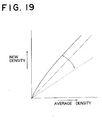
- the average density in secondary scanning direction can also be converted as shown in Fig. 19.
- the present invention is not limited to the specific embodiments, but when the image data processing circuit 100 is replaced by the image data processing circuit 150 composed of the color scanner 151, the A/D converter 152, the density converter 153, the masking UCR circuit 154 and the like, and the image density data is inputted into the processing circuit 150 from the scanner and the image is processed in the circuit, the present invention can be adopted to other image forming apparatus such as a copying apparatus and the like.
- the entire image frame can be changed uniformly by an external command such as a character, photographic mode and the like.
- This method is adopted to an device, like a light emitting panel EL, in which the pulse width can be modulated in the subsidiary scanning direction.
- a phase of the reference wave signal is selected from image data subjected to RE processing wherein, for an objective pixel located in a specific density range, the objective pixel is divided into small pixels and with regard to the density of the small pixel, the density of the objective pixel is distributed in accordance with distribution of density data of adjoining pixels including the objective pixel, recording position modulation signals obtained by modulating the density signals of the objective pixel with the reference wave are generated, and recording position modulation is not conducted for the low density area and high density area.
- the image discrimination is conducted by the image discrimination circuit; when the image exists in the character region, the recording position modulation is conducted by the reference wave of a short period; and when the image exists in the halftone region, the recording position modulation is conducted by the reference wave of a long period, thus, an excellent color image forming apparatus, in which sharpness can be increased without causing change in color tone of the color image which is generated from the scanner, CG, or font data, can be provided.
- the aforementioned method shows the case where the number of recording beams for the pixel is three. Further, the following methods can be conducted: the pixel can be scanned by one or two recording beams; the recording position modulation can be conducted only in the primary scanning direction, When a high ⁇ photoreceptor is used for the color image forming apparatus, effects can be further improved.
- FIG. 4 represents a perspective view showing a schematic constitution of the image forming apparatus in the present example.
- an area of a dot is changed by pulse width modulation stated above for indication of gradation.
- image signals prepared by a computer as described above or read by a scanner when an edge portion of high image density interferes with a reading pixel, the signals on the relevant pixel become the same as medium density of a uniform image.
- a recording dot is formed isolatedly at the center of a pixel for both recording at edge portions and recording at a halftone area. Therefore, only expression with rough resolution has been all done by the pulse modulation system.
- recording position modulation that displaces, in the primary scanning direction, the position of an electrostatic latent image by means of a recording dot is conducted and formation of a fine dot by means of a plurality of laser beam scanning operations for one pixel is conducted for obtaining an image with improved resolution.
- Scanning optical system 430 converts, by means of collimator lens 432, a laser beam emitted from semiconductor laser alley 431 into a plurality of parallel laser beams as parallel beams.
- the laser beam is subjected to deflection through reflection by means of rotary polygon mirror 434 that rotates at a constant speed and then advances, through f ⁇ lens 435 and cylindrical lenses 433 and 436, to the surface of photoreceptor 401 charged uniformly where the laser beam is focused in a spot shape to become a plurality of laser spots through scanning for imagewise exposure.
- the f ⁇ lens 435 is a correcting lens for achieving beam scanning at a constant speed and the cylindrical lenses 433 and 436 are correcting lenses for correcting fluctuations of a spot position caused by accidental inclination of the surface of the rotary polygon mirror 434.
- one of reference waves to be combined with image density data is one having a phase difference and the other is a group og a plurality of reference waves each having a different DC component, and image forming is conducted by modulated image signals obtained by combining selectively the image density data and a specific reference wave selected from reference waves.
- a high ⁇ photoreceptor is especially effective for forming a latent image by responding accurately to the above-mentioned modulated image signals.
- Fig. 22 is a block diagram showing an example of an image processing circuit used in the image forming apparatus in the third example of the invention
- Fig. 3 is a block diagram showing a modulating circuit in the present example.
- modulated signal generating circuit 200 in the present example, image density data for a unit of one scanning line are read from image density data storage circuit 210, and from the continuous density data for the unit of one scanning line, image density data corresponding to an edge portion are detected by edge detection circuit 240, and there are generated modulated signals wherein a pulse width is modulated by modulation circuits 260A - 260C employing a reference wave having a phase difference in the direction of the edge, in the case of a character reproduction area including characters and line images.
- modulated signals are generated by the modulation circuits 260A - 260C employing a reference wave having different DC components and modulating a laser beam that scans the central portion of a pixel. These modulated signals are sent to raster scanning circuit 300 having a driving means for semiconductor laser array 431 that has three emitters.
- the modulated signal generating circuit 200 is composed of image density data storage circuit 210, reading circuit 220, latch circuit 230, edge detection circuit 240, image discrimination circuit 241, select circuits 250A - 250C, modulating circuits 260A - 260C, reference clock generating circuit 280, triangular wave generating circuit 290, delay circuits group 291 and DC component addition circuit 292.
- the reading circuit 220 reads, with index signals as a trigger, continuous image density data for a unit of one scanning line from the image density data storage circuit (page memory) 210, synchronizing with reference clock DCK0, and sends them to the edge detection circuit 240 and latch circuit 230.
- the latch circuit 230 is a circuit that latches image density data only when the edge detection circuit 240 and the select circuits 250A - 250C are processing.
- the triangular wave generating circuit 290 conducts wave-forming for a reference triangular wave having the same cycle as that of a pixel clock based on the reference clock DCK0.
- the delay circuits group 291 represents a circuit that generates a plurality of triangular waves each having a phase difference of 1/n cycles against a reference triangular wave.
- a triangular wave having a phase delayed by 1/3 cycles against the reference clock DCK0 is generated from terminal ⁇ 1
- a triangular wave having a phase delayed by 2/3 cycles, namely advanced by 1/3 cycles, against the reference triangular wave is generated from terminal ⁇ 2.
- the edge detection circuit 240 finds a difference value by differentiating successively image density data of a unit of one scanning line inputted continuously, reads from a built-in memory the selected signals corresponding to the difference value, and sends them to select circuits 250A - 250C.
- the aforementioned difference value means "+1" when the differentiated value is not less than ⁇ , and it means "-1" when the differentiated value is not more than - ⁇ .
- a positive or negative sign for the difference value represents the direction of an edge, and the positive sign means that the edge is located at the left side in the scanning line direction, while the negative sign means that the edge is at the right side in the scanning line direction.
- the difference value is assumed to be "0".
- the image discrimination circuit 241 is a circuit which judges whether continuous image density data read from reading circuit 220 belongs to a character reproduction area or to a halftone reproduction area. When discrimination is for the character reproduction area, signals for causing DC components added to a reference triangular wave to be zero are sent to DC component adding circuit 292, while when discrimination is for the halftone reproduction area, signals for adding predetermined DC components to a reference triangular wave are sent to the DC component adding circuit 292.
- image discrimination may be conducted based on an extent of a change in density of an objective pixel and its surroundings and on existence of an edge.
- specific density for example, not more than 0.2 in terms of recorded density
- the select circuits 250A - 250C output triangular waves each having a phase different in accordance with selected signals from edge detection circuit 240 to modulation circuits 260A - 260C.
- a reference triangular wave is sent
- a triangular wave delayed be 1/3 cycles is sent
- a triangular wave advanced by 1/3 cycles are sent, all to terminal T of the modulation circuits 260A - 260C.
- a triangular wave to which predetermined DC components have been added is sent from the select circuit 250B to modulation circuit 260B.
- the modulation circuits 260A - 260C have the same circuit constitution as shown in Fig. 3 mentioned above, and each of them is composed of a D/A converter 261 and comparator 262. Image density data sent through latch circuit 230 are subjected to D/A conversion made by D/A converting circuit 261 in the modulation circuits 260A - 260C synchronizing with reference clock DCK0, and they are compared with a reference wave of a triangular wave inputted from terminal T, thus pulse-width-modulated signals are obtained in the modulation circuits 260A - 260C.
- Figs. 23 (a) - (h) represent time charts each showing a signal at each portion in the modulated signal generating circuit in the present example.
- FIG. 23 shows a part of image density data for one scanning line read from page memory 210 with index signals as a trigger based on reference clock DCK0 which have been converted into analog values by D/A converting circuit 261.
- the digital image density data for one scanning line are sent from the reading circuit 220 to edge detection circuit 240, image discrimination circuit 231 and latch circuit 230 simultaneously.
- edge detection circuit 240 image discrimination circuit 231 and latch circuit 230 simultaneously.
- FIG. 23 shows the state of edge detection in the primary scanning direction in edge detection circuit 240, and it indicates a differentiated value in the primary scanning direction.
- a differentiated value exceeds the specific value ⁇
- discrimination is made for an edge area, and the direction of the edge is judged depending on whether the sign of the value is positive or negative.
- the outputted value of "0" means that image density data on the same level are existing continuously. This output signal is sent to select circuits 250A - 250C based on reference clock DCK0.
- the latch circuit 230 latches only for the period necessary for the edge detection circuit 240 and select circuits 250A - 250C to process, and sends to the modulation circuits 260A - 260C.
- the select circuits 250A - 250C send triangular waves having different phases as mentioned above from an output terminal to the modulation circuits 260A - 260C based on selected signals from the edge detection circuit 240.
- a reference wave on the occasion that the value outputted from edge detection circuit 240 in the modulation circuits 260A - 260C is plus is shown in (c).
- the reference wave is a triangular wave whose phase is delayed from that of the reference triangular wave by 1/3 cycles.
- the phase of the obtained modulated signals which are the output signals from modulation circuits 260A - 260C is delayed by 1/3 cycles as shown in (f), which is different from an occasion wherein pulse-width modulation is made with a reference triangular wave.
- the modulated signals shown with dotted lines are output signals obtained by modulating with a triangular wave having no delayed phase.
- Fig. 23 (d) shows modulation operations in the case where an output value from edge detection circuit 240 in the modulation circuits 260A - 260C is "0", and modulated signals with a reference phase as shown in (g) wherein image density data corresponding to the period when selected signals from the edge detection circuit 240 are "0" are modulated by a reference triangular wave are outputted to the modulation circuits 260A - 260C.
- Fig. 23(e) shows modulation operations in the case where an output value from edge detection circuit 240 in the modulation circuits 260A - 260C is minus, and image density data corresponding to the period when selected signals from the edge detection circuit 240 show the negative value are inputted, and a reference wave is represented by a triangular wave whose phase is advanced by 1/3 cycles. Due to this, comparator 262 compares, and modulated signals with pulse-width modulation whose phase is advanced by 1/3 cycles as shown in (h) are outputted.
- the modulated signal generating circuit 200 in the present example outputs modulated signals for a unit of one scanning line wherein a position of an edge portion has been modulated in the primary scanning direction directly to laser drivers 301A - 301C or through ⁇ -delay circuit 311 or 2 ⁇ -delay circuit 312, and thereby causes semiconductor laser array 431 to oscillate.
- Fig. 24 is an illustrated diagram showing how a latent image in a character reproduction area is formed with modulated signals from the modulated signal generating circuit 200.
- a dot of an edge portion is deviated toward an edge in the primary scanning direction to be recorded.
- 1-1 shows a line of the aforementioned latent image formed by laser spot sa
- 1-2 shows a line of the latent image formed by laser spot sb
- 1-3 shows a line of the latent image formed by laser spot sc.
- Nest scanning lines are represented by 2-1, 2-2 and 2-3.
- select circuits 250A - 250C When image discrimination circuit 241 judges to be a halftone reproduction area, select circuits 250A - 250C output all reference triangular waves to the modulation circuits 260A - 260C because the result of edge detection shows "0". With signals of the image discrimination circuit 231, however, DC component adding circuit 292 sends to select circuit 250B the triangular wave wherein predetermined DC components are added to a reference triangular wave.
- Fig. 25 shows each reference wave in the above case, and one-dot chain lines show image density signals.
- an electrostatic latent image formed on photoreceptor 401 takes a form that is close to a rhombic form wherein a recorded width at a central portion is long as shown in Fig. 26, and uniform halftone images having no longitudinal stripes are obtained.
- image processing circuits mentioned above have been explained with an example of a laser printer, the invention is not limited only to this.
- image data processing circuit 150 comprising color scanner 151, A/D converting circuit 152, density conversion circuit 153, and masking UCR circuit 154 so that the image data processing circuit may take charge of input of image density data from the scanner and of image processing, it may be applied to other image forming apparatus such as a copying machine or the like.
- Fig. 27 represents a diagram showing a reference wave of a halftone reproduction area used in the fourth example of the invention.
- a cycle of the reference wave one cycle corresponds to two pixels and its DC component grows greater as a scanning line advances in the sequence of 1-1, 1-2 and 1-3, while, the DC component decreases as the next scanning line advances in the sequence of 2-1, 2-2 and 2-3, which repeats.
- the reference wave of a character reproduction area is the same as in the third example, and its cycle corresponds to one pixel.
- an electrostatic latent image of a halftone reproduction area formed takes a rhombic form close to a halftone dot as shown in Fig. 28 and further uniform halftone images having no longitudinal stripes are obtained.
- the reference wave of a character reproduction area is the same as in the third example, and a recording position is modulated and a profile may be reproduced sharply.
- the fifth example is the same as the third example as far as a character reproduction is concerned.
- dots corresponding to a halftone dot with a screen angle can be formed through a means wherein a plurality of reference waves having different phases are used for modulation of recording positions. For example, it is possible to improve color uniformity and to prevent occurrence of moire fringes with screen angles of 45° for a yellow image, 26.6° for a magenta image, -63.4° for a cyan image and 0° for a black image.
- a dot image corresponding to a halftone dot with a screen angle of 26.6° may be formed.
- a screen angle of 45° may be obtained.
- the present invention provides, as described above, an image forming apparatus comprising a semiconductor laser array oscillated by image density data modulated by reference wave signals to form an electrostatic latent image on an image forming member, wherein there is provided a modulation means in which a size of a recording dot and a recording position in the primary scanning direction are changed depending on image density by combining selectively image density data and a reference wave with a different phase based on an edge detection circuit and its detection results, and a dot in a rhombic shape is formed by changing DC components of a reference wave used or causing one cycle to correspond a plurality of pixels, so that an image formed by scanner, CG and font data may have no longitudinal stripes and have high sharpness to be an excellent image.
Abstract
Description
- In the present invention, distribution of adjoining pixels is reflected in density distribution of objective recording pixels so that high quality recording can be conducted. The present invention relates to a color image forming apparatus in which: one matrix pixel image data is divided into small pixels m x n (the width x the length) considering the adjoining pixel data, and after that, the center of gravity of each line is found; the phase of the reference wave is deviated according to the center of gravity; and dot recording composed of n small scanning lines is conducted by the modulated signal of the pixel density data modulated by the reference wave signal so that a character and a halftone image can be reproduced. The recording apparatus of the present invention is used for a printing apparatus or a displaying apparatus.
- In the field of image forming apparatus using the electrophotographic method, a digital halftone image is reproduced in the following manner: an original image is read by a scanner to get on image signal; and image density data in which the image signal is gradation-corrected, A/D converted, and shading-corrected, is modulated by a reference signal and thus digital image is obtained.
- When an original image is read by the scanner, an edge portion of the image is read in a halftone density due to the aperture of a solid state image pick-up element installed in the scanner. When a latent image is formed on a photoreceptor with an image density data obtained from image signals, recording pixels corresponding to the edge portion of the latent image are recorded in recording pixels on an average basis. Therefore, the sharpness of the recorded image is lowered. For this phenomenon, in the past, there has been known a method to apply an MTF correction by means of image-sharpening by the use of a differential filter, or a Laplacian filter on image signals. In this method, however, edge portions only are enhanced, and uniformity of halftone images is relatively lowered.
- On the other hand, even when an interpolated character or figure is formed from computer graphic (C.G.) data or font data, a similar problem is caused. That is, when the edge portion is interpolated smoothly with the intermediate density using the interpolated data, a recording pixel corresponding to the edge portion is recorded in pixels as average density, and thereby the resolution is lowered in the same way as the aforementioned.
- For the reasons mentioned above, intermediate density processing, which effectively operates on the edge portion of the image, is required.
- Further, when intermediate density processing is conducted on each color in a color image forming apparatus, there occurs the problem in which color tone is varied, or characters become not sharp.
- Further, the invention relates to an image forming apparatus wherein dot-recording is made for reproduction of characters and halftone images by a laser diode oscillated by modulation signals in which density data are modulated by reference signals.
- In view of the foregoing problems, an object of the present invention is to provide an image forming apparatus in which resolution of the image, which is formed from scanner data, C.G data, font data, or the like, is improved, and high quality images having no longitudinal streaks are recorded.
- In the first constitution of an image forming apparatus of the invention capable of conducting high density pixel recording with density data of small pixels in an objective pixel determined based on density data of pixels adjoining the objective pixel, the objective pixel determines a recording position for each color based on density distribution of the adjoining pixels when the recording position of each color is modulated in the primary scanning direction and secondary scanning direction based on density distribution of both the objective pixel and the adjoining pixels. In this type of image forming, preferable resolution and gradation matching an image can be realized by making the cycle of a reference wave to be variable corresponding to the image. Further, in the first constitution of an image forming apparatus of the invention, there are provided a means for image judgment on the objective pixel mentioned above and a means which modulates a recording position using a reference wave with a long cycle when an image is judged to be a halftone area under the image judgment, and modulates the recording position using a reference wave with a short cycle when an image is judged to be a character area.
- In the second constitution of an image forming apparatus of the invention, a plurality of scanning operations are conducted for a unit pixel and an image is formed with a scanning position deviated by a selectable reference wave for a character reproduction area and with a scanning width changed by a selectable reference wave for a halftone reproduction area.
- With regard to a reference wave cycle for the halftone reproduction area mentioned above, the aforementioned image forming apparatus wherein a plurality of pixels are used and a phase of a reference wave differs for each color is a preferable embodiment.
- Fig. 1 is a block diagram of an image processing circuit in the first example of an image forming apparatus of the invention, Fig. 2 is a block diagram showing an example of a determination circuit for a reference wave phase in the circuit shown in Fig. 1, and Fig. 3 is a block diagram showing an example of a modulation circuit in the circuit shown in Fig. 1. Fig. 4 is a perspective view showing the general constitution of an image forming apparatus of the invention. Fig. 5 a diagram illustrating the RE process used for a determination of a reference wave phase, and Fig. 6 is a diagram showing an example wherein an objective pixel of the RE process is divided into the number of 3x3 and P is assumed to be 0.5 (P=0.5). Fig. 7 is a diagram showing an example wherein an objective pixel for the RE process is divided into the number of 2x2, and Fig. 8 is another example showing the same occasion as in Fig. 7. Fig. 9 is a diagram for illustrating the phase displacement for a reference wave in the case of a character area. Fig. 10 is a time chart showing each signal in the case of a character area for a modulation signal generation circuit in the example shown in Fig. 1. Fig. 11 is a diagram for illustrating the phase displacement for a reference wave in the case of a halftone area. Fig. 12 is a time chart showing each signal in the case of a halftone area for a modulation signal generation circuit in the example shown in Fig. 1. Fig. 13 is a graph showing the characteristics of a high γ photoreceptor used in the present example, and Fig. 14 is a cross-sectional view showing the concrete example of constitution for the high γ photoreceptor used in the present example. Fig. 15 is a diagram showing a semiconductor laser alley in the example shown in Fig. 4, and Fig. 16 is a diagram showing a scanning locus of a laser spot by means of a semiconductor laser alley shown in Fig. 13. Fig. 17 is a graph showing an example of the relation between driving current for a semiconductor laser and laser radiation output. Fig. 18 is a graph showing an example of an occasion wherein the relation between a center of gravity in the primary scanning direction of a small scanning line and a recording position is changed. Fig. 19 is a graph showing an example of an occasion wherein average density in the secondary scanning direction of a small scanning line is converted. Fig. 20 is a block diagram showing an image processing circuit in the second example of the invention, and Fig. 21 is a block diagram showing a phase determination circuit for a reference wave in Fig. 20. Fig. 22 is a block diagram showing a modulation signal generation circuit in the third example, and Fig. 23 is a time chart showing each signal in the case of a character reproduction area for a modulation signal generation circuit in the third example. Fig. 24 is an illustrative diagram wherein a latent image in a character reproduction area is formed by modulation signals in the third example. Fig. 25 is a diagram showing an example of a triangular wave which is a reference wave of a halftone reproduction area in the third example, and Fig. 26 is an illustrative diagram wherein a latent image in a halftone reproduction area is formed by modulation signals in the third example. Fig. 27 is a diagram showing a reference wave used in the fourth example of the invention, and Fig. 28 is a diagram showing an electrostatic latent image in the fourth example of the invention. Fig. 29 is a diagram showing an electrostatic latent image in the fifth example of the invention.
- The constitution of
image forming apparatus 400 which is an example of the invention will be explained as follows. Fig. 4 is a perspective view showing general constitution of the image forming apparatus in the present example. - A color image can be obtained by the
image forming apparatus 400 as follows:
After a photoreceptor has been uniformly charged, a dot-shaped electrostatic latent image is formed thereon by a spot light which has been pulse-modulated in accordance with a modulation signal obtained through differential amplification between an analog image density signal which can be obtained by D/A-converting a digital image density signal sent from a computer or a scanner, and a reference signal, and this electrostatic latent image is reversely developed by toner so that a dotshaped toner image is formed. The aforementioned charging, exposing and developing processes are repeatedly conducted so that a color toner image can be formed on the surface of a photoreceptor, and then the obtained color toner image is transferred, separated and fixed. - The
image forming apparatus 400 is composed of, a drum-shaped photoreceptor 401 (hereinafter, referred to as a photoreceptor) which is rotated in the direction of an arrow, ascorotron charger 402 which gives a uniform electric charge on theaforementioned photoreceptor 401, anoptical scanning system 430, developing units 441 - 444 which are loaded with yellow, magenta, cyan and black toners, ascorotron transfer unit 462, aseparator 463, afixing roller 464, acleaning unit 470, and adischarger 474. - Fig. 14 is a diagram showing an example of a specific structure of a
high γ photoreceptor 401 used in the present example. - As illustrated in Fig. 14, the
photoreceptor 401 is composed of a conductive support 401A, an intermediate layer 401B, and aphotosensitive layer 401C. The thickness of thephotosensitive layer 401C is 5 - 100 µm, and preferably 10 - 50 µm. Thephotoreceptor 401 is made of an aluminum drum-shaped conductive support 401A. On the aforementioned support 401A is formed the intermediate layer 401B of 0.1 µm in thickness, which is made from ethylene-vinyl acetate, and on the intermediate layer 401B is provided thephotosensitive layer 401C, the thickness of which is 35 µm. - A drum of 150 mm in diameter which is made from aluminum, steel or copper is used for the conductive support 401A. A belt-shaped conductive support is also used which is made in such a manner that a metallic layer:is vapor-deposited or laminated on a paper or a plastic film. A metallic belt made from nickel by means of electroforming may be also used. It is preferable that the intermediate layer 401B can endure a high potential charging of ±500 - ±2000V as a photoreceptor, and it is further preferable that the intermediate layer 401B is provided with a hall mobility so that the flow of electrons from the
conductive support 401C can be prevented when it has been charged positive, and so that an excellent light decay characteristic can be obtained due to the avalanche effect. Therefore, it is preferable that a positive charging type of electric charge conveyance material which has been disclosed in Japanese Patent Application 188975/1986 by the inventors, is added to the intermediate layer 401B by not more than 10 weight percent. - The following resins which are commonly used in a light sensitive layer for electrophotography use, are used for the intermediate layer 401B.
- (1) Vinyl polymer such as polyvinyl alcohol (poval), polyvinyl methyl ether, polyvinyl ethyl ether, and the like
- (2) Vinyl polymer containing nitrogen such as polyvinyl amine, poly-N-vinyl imidazole, polyvinyl pyridine, polyvinyl pyrrolidone-vinyl acetate copolymer, and the like
- (3) Polyether polymer such as polyethylene oxide, polyethylene glycol, polypropylene glycol, and the like
- (4) Acrylic acid polymer such as polyacrylic acid and its polymer, polyacrylic amide, poly-β-hydroxy ethyacrylate, and the like
- (5) Metaacrylic acid polymer such as polymetaacrylic acid and its salt, polymetaacrylic amide, polyhydroxy propylmetaacrylate, and the like
- (6) Ether cellulose polymer such as methyl cellulose, ethyl cellulose, carboxymethyl cellulose, hydroxymethyl cellulose, hydroxypropylmethyl cellulose, and the like
- (7) Polyethylene imine polymer such as polyethylene imine and the like
- (8) Polyamino acid such as polyalanine, polyserine, poly-L-glutamic acid, poly-(hydroxyethyl)-L-glutamine, poly-δ-carboxymethyl-L-cysteine, polyproline, lysine-thylosin copolymer, glutamic acid-lysin-alanine copolymer, silkfibroin, casein, and the like
- (9) Starch and its derivative such as starch acetate, hydroxyne ethyl starch, starch acetate, hydroxyethyl starch, amine starch, phosphate starch, and the like
- (10) Polymer soluble in a mixed solvent of water and alcohol such as soluble nylon of polyamide, methoxymethyl nylon (8 type nylon), and the like.
- The
photosensitive layer 401C is formed by coating a coating agent on an intermediate layer and after that the coated layer is dried and heat-treated if necessary, wherein the coating agent is prepared as follows: basically, electric charge conveyance material is not added into thephotosensitive layer 401C; phthalocyanine fine particles of 0.1 - 1µm in diameter composed of a photoconductive pigment, an antioxidant and a binder resin are mixed and dispersed in a solvent. - In the case where a photoconductive material and electric charge conveyance material are jointly used, a photosensitive layer is composed as follows: a photoconductive material composed of a phtoconductive pigment and a small amount of electric charge conveyance material, the amount of which is not more than 1/5 of the aforementioned photoconductive pigment, or preferably 1/1000 - 1/10 (weight percent) of the pigment, and an antioxidant are dispersed in a binder resin. When a high γ photoreceptor described above is utilized, a sharp latent image can be formed although the diameter of a beam is spread, so that a recording of high resolution can be effectively conducted.
- In this embodiment, color toner images are superimposed on a photoreceptor. Accordingly, a photoreceptor, the spectral sensitivity of which is on the infrared side, and a semiconductor laser of infrared light are used so that the beam sent from the optical scanning system can not shade the color toner image.
- The light decay characteristic of the high γ photoreceptor of the present invention will be explained as follows.
- Fig. 13 is a graph showing the outline of a high γ photoreceptor. In Fig. 5, V₁ is a charging potential (V), V₀ is an initial potential (V) before exposure, L₁ is the amount (µJ/cm²) of light of the illuminated laser beam which is required to reduce initial potential V₀ to 4/5, and L₂ is the amount (µJ/cm²) of light of the illuminated laser beam which is required to reduce initial potential V₀ to 1/5.
- A preferable range of L₂/L₁ is 1.0 < L2/L1 ≦ 1.5.
- In this embodiment, V₁ = 1000(V), V₀ = 950(V), and L₂/L₁ = 1.2. The photoreceptor potential of the exposure section is 10V.
- Assume that the light sensitivity is E1/2 at the position corresponding to the middle period of exposure in which the initial potential (V₀) is decayed to 1/2, and that the light sensitivity is E9/10 at the position corresponding to the initial period of exposure in which the initial potential (V₀) is decayed to 9/10, then a photoconductive semiconductor satisfying the following inequality is selected.

Preferably
In this case, light sensitivity is defined as the absolute value of potential drop with regard to a minute amount of exposure. - In the light decay curve of the
photoreceptor 401, the absolute value of the differential coefficient of the potential characteristic is decayed a little when the amount of light is small, and decayed sharply as the amount of light is increased as shown in Fig. 13. Specifically, in the initial period of exposure of the light decay curve as shown in Fig. 13, the sensitivity characteristic is bad for a certain period of time L₁. However, in the middle period of exposure and thereafter to the end, the light sensitivity is highly increased so that the light decay curve goes downward almost linearly, in other words, the photoreceptor shows a super-high γ characteristic. It can be considered that thephotoreceptor 401 acquires a high γ characteristic using an avalanche phenomenon under a high charging potential of +500 - +200V. It can be considered as follows. That is, the carrier generated on the surface of the photoconductive pigment in the initial stage of exposure, is effectively trapped by an interface layer between the pigment and coated resin, so that light decay is positively restricted. As a result, a very sharp avalanche phenomenon is caused in the middle stage of exposure and thereafter. - Next, a color image forming apparatus of the present invention will be explained as follows. In the color image forming apparatus, an objective matrix pixel of the image density data is composed of small pixels m × n (width × length), and a distribution of the density data of adjoining pixels including the objective pixel, is replaced with the distribution of small pixels m x n in one pixel, and the image is formed by the following method: a position in which dots of n rows are written is displaced when a phase of a reference wave in each row of small pixels is displaced according to image density data of small pixels obtained by distributing data of the objective pixel multiplied by constant P corresponding to the distribution. Displacement of the position in which dots are written will be referred to as recording position modulation, hereinafter. Further, processing to convert the image density data of the objective pixel into the image density data of small pixels obtained by dividing the objective pixel into m × n, will be referred to as resolution enhancing processing (RE processing), hereinafter. Due to RE processing, high density recording can be conducted. In this case, a high γ photoreceptor is specifically effective in order to form a latent image corresponding exactly to the reference wave.
- In this invention, RE processing is conducted when ① the image density data of the objective pixel is not less than a first threshold value, that is, not less than the specific density, namely the first threshold value. In many portions of an area corresponding to a highlight portion, RE processing is not conducted on a background portion of a document, and small pixels m × n are set to have a uniform density. In the case of CRT, this data display can be possible.
- However, in the case of laser recording which will be described later, it is difficult to display the data uniformly, and therefore, the reference wave whose density center exists in the center of the image density, is selected. Due to the aforementioned, uniformity in the highlight portion can be kept, and a noisy image can be prevented from occurring.
- ② In the case of high density and a steep density gradient, when a reference wave whose density recording position does not exist in the center is selected, dots are formed in the manner that they overlap with the adjoining pixel.
- In order to prevent a density change and recording dot blocking between pixels, when the image density data of the objective pixel is not less than a specific second threshold value, and also in a high density portion, a reference wave whose density center exists in the center of the image density, is selected.
- Since a uniform display can be conducted in the case of CRT, the densities of small pixels m × n are processed as a uniform density. That is, RE processing is not conducted.
- In a color image forming apparatus in which high density image recording is conducted according to density distribution data in the objective pixel which is determined corresponding to density data of the pixels adjoining the objective pixel, a color image forming apparatus which is characterized as follows is preferable: when a specific density data of the objective pixel is not less than the first threshold value, recording position modulation is conducted according to the determined density distribution; or when a specific density data of the pixel is not more than the second threshold value recording position modulation is conducted according to the determined density distribution.
- Fig. 5(a) is a plan view in which the adjoining pixels including the objective pixel m5 are expressed as m1 to m9 when the objective pixel is defined as m5, and the objective pixel m5 is divided into 3 × 3 small pixels. Fig. 5(b) is an enlarged view in which each small pixel is expressed by s1 to s9 when the objective pixel is divided into small pixels of 3 × 3. m1 to m9 and s1 to s9 also express the density of each portion.
- RE processing will be explained in detail as follows. Taking the example of the case where the objective pixel m5 is divided into 3 × 3 small pixels, density of a small pixel si is determined by the following equation.

- Where i = 1, 2, ····, 9, and P is a constant, which is called strength for RE processing, and in which the range of 0.1 to 0.9 is used, and A is the sum total of m1 to m9.
- In the above equation, a term of (9 × m5 × P × mi/A) expresses a density in which the density of the objective pixel m5 multiplied by P is distributed to each small pixel according to density ratio of the adjoining pixels, and the term (1-P) × m5 expresses a density in which the residual density of the objective pixel m5 is distributed equally to each small pixel, so that an element of unsharpness is taken into the equation.
- Fig. 6 is an illustration showing an example in which the objective pixel m5 is divided into 3 × 3 small pixels, and P = 0.5. Fig. 6(a) is an illustration showing an example of the density distribution of the adjoining pixels including the objective pixel m5. Fig. 6(b) is an illustration showing the density distribution in the objective pixel m5 which is calculated by P = 0.5.
- Fig. 7 and Fig. 8 show an example in which the objective pixel m5 is divided into 2 × 2 small pixels.
- Fig. 7(a) is an illustration showing an example in which the objective pixel m5 is divided into 2 × 2 small pixels. Fig. 7(b) is an illustration showing an example of the adjoining pixels relating to small pixels s1 to s4 in the objective pixel.
- Density of s1, s2, s3, and s4 is calculated according to
Equation 1. -


where A is the total sum of m1 to m9. - Fig. 8(a) is an illustration showing another example in which the objective pixel m5 is divided into 2 × 2 small pixels. Fig. 8(b) is an illustration showing another example of the adjoining pixels relating to small pixels s1 to s4 in the objective pixel. Density calculation of s1, s2, s3, and s4 is conducted according to
Equation 2. -


where A is the total sum of m1 to m9. - Fig. 1 is a block diagram showing an example of an image processing circuit which is used in a color image forming apparatus of the present invention (an example in which the objective pixel is divided into 3 × 3). Fig. 2 is a block diagram showing a circuit for determining a reference wave phase and, Fig. 3 is a block diagram showing a modulation circuit in the present example.
- An image processing circuit 1000 of this embodiment is a circuit composing a drive circuit of an optical scanning system. The image processing circuit 1000 is composed of an image
data processing circuit 100, a modulationsignal generating circuit 200, and araster scanning circuit 300. - The image
data processing circuit 100 is a circuit to interpolate the edge portion of font data and output the obtained data. The imagedata processing circuit 100 is composed of aninput circuit 110, fontdata generating circuit 120, fontdata storing circuit 130, and interpolationdata generating circuit 140. A character code signal, size code signal, position code signal, and color code signal are sent from theinput circuit 110 to the fontdata generating circuit 120. The fontdata generating circuit 120 selects an address signal from 4 kinds of input signals and sends the selected signal to the fontdata storing circuit 130. The fontdata storing circuit 130 sends font data corresponding to the address signal to the fontdata generating circuit 120. The fontdata generating circuit 120 sends the font data to the interpolationdata generating circuit 140. The interpolationdata generating circuit 140 interpolates a zig-zag and jump of the image density data which are caused on the edge of font data using an intermediate density, and sends the interpolated data to the image densitydata storing circuit 210 composed of a frame memory. Concerning the color to be generated, the corresponding data is converted to the density data of yellow (Y), magenta (M), cyan (C), and black (BK) in accordance with a color code. In the way described above, the font is bit-map-developed in each frame memory under the condition that the shape is the same and the density ratio of each color is different. - The
modulation signal generator 200 is composed of the image densitydata memory circuit 210, a read-out circuit 220, alatch circuit 230, animage discrimination circuit 231, anMTF correction circuit 232, aγ correction circuit 233, circuit for determiningreference wave phase 240,select circuits 250A to 250C,modulation circuits 260A to 260C,reference clock generator 280, triangularwave generating circuit 290 anddelay circuits group 291. - The image density
data storing circuit 210 is usually a page memory (which is referred to as apage memory 210, hereinafter). That is, the image densitydata storing circuit 210 is a RAM which stores the data by the unit of a page, and at least has a capacity of storing a page of multi-value image density data. When the apparatus is used for a color printer, the apparatus must be provided with a storage capacity enough to store the image density signal corresponding to a plurality of colors, for example, yellow, magenta, cyan and black. The read-out circuit 220 reads out continuous image density data of every one scanning line, which is continued in synchronization with the standard clock DCK₀ from the image density data memory circuit (page memory) 210, and sends it to the RE processing circuit, theimage discrimination circuit 231, andMTF correction circuit 232, wherein an index signal is used as a trigger. - The
latch circuit 230 is a circuit which latches the image density data only when the processing in the circuit for determiningreference wave phase 240. - The
reference clock generator 280 is a pulse generating circuit, and generates a pulse signal with a cycle period identical to that of the pixel clock, and sends it to the read-out circuit 220, triangularwave generating circuit 290, developingcircuits group 291 andmodulation circuits 260A - 260C. This clock is called reference clock DCK₀ for convenience' sake. - The numeral 290 represents a triangular wave generation circuit and it forms, based on reference clock DCK₀, waveforms for both reference triangular wave φ₀′ which is a reference wave whose cycle is the same as that of a pixel clock and triangular wave φ₀˝ which is a reference wave whose cycle is two times that of a pixel clock. Further, in
delay circuit group 291, a plurality of clocks DCK₁′ - DCK₄′ and DCK₁˝ - DCK₄˝ each having a phase difference of a constant period of cycle (1/6 cycles in the present example) against the reference clock DCK₀ and the clock whose cycle is two times that of a reference clock are generated, and based upon this, it outputs triangular waves φ₁′ - φ₄′ and φ₁˝ - φ₄˝ (in this example, triangular waves φ₁′ and φ₁˝ whose cycle is ahead by 1/6 cycles, triangular waves φ₂′ and φ₂˝ whose cycle is ahead by 2/6 cycles, triangular waves φ₃′ and φ₃˝ whose cycle is behind by 1/6 cycles and triangular waves φ₄′ and φ₄˝ whose cycle is behind by 2/6 cycles). -
Select circuits 250A - 250C have input portion for triangular waves φ₁′ - φ₄′ and φ1˝ - φ4˝ each being different, in terms of phase, from the aforementioned reference triangular waves φ₀′ and φ₀˝, and one of the aforementioned triangular waves is selected by selection signals coming from reference wavephase determination circuit 240 which will be stated later, and is sent to input terminal T ofmodulation circuit 260A - 260C. - As illustrated in Fig. 3, the
modulation circuits 260A - 260C have the same circuit structure. The modulation circuits are provided with the D/A-conversion circuit 261, thecomparator 262, and input portion T for the reference triangular wave φ₀′ and triangular waves having phases each being deviated by 1/6 cycles as well as triangular wave φ₀˝ having a double cycle and triangular waves having phases each being deviated by 1/6 cycles. The image density data inputted throughlatch circuit 230 is D/A-converted by the D/A-conversion circuit 261 synchronously with reference clock DCK₀, and the modulated image density data are compared with a reference wave that is the trianular wave inputted fromselect circuits 250A- 250C. Thus, pulse-width-modulated signals are obtained. -
Image discrimination circuit 231 selects a reference wave from φ₀′ - φ₄′ for a character area and from φ₀˝ - φ₄˝ for a halftone area. - As shown in Fig. 2, the circuit for determining
reference wave phase 240 is composed of a oneline delay circuit 242, a oneclock delay circuit 243, and anarithmetic processing circuit 241. The oneline delay circuit 242 operates as follows: the image density data of the first one scanning line of three scanning lines of the image density data in which one scanning line is sent at a time is delayed by two line scanning time periods by the oneline delay circuit 242; the image density data of the second one scanning line is delayed by one line scanning time period by thecircuit 242; and the image density data of the last one scanning line is not delayed. Further, each image density data is delayed for the time of two reference clocks or one reference clock by the oneclock delay circuit 243, and all image density data of the pixels, which include the objective pixel and adjoin the pixel, are sent at the same time to thearithmetic processing circuit 241. - In the
arithmetic processing circuit 241, the image density data of the small pixel is obtained by the RE processing. - The image density data of the obtained small pixel is divided into a small scanning line including s1, s2, s3···shown in Fig. 5, the small scanning line including s4, s5, s6···, and the small scanning line including s7, s8, s9 ···, and one scanning line of the original pixel corresponds to these three scanning lines of the small pixels.
- The
arithmetic processing circuit 241 calculates average density of each small scanning line and the position of gravity center of the density data in each small scanning line, outputs the average density data to emission output oflaser drivers 301A to 301C and outputs different selected signals based on the position data of gravity center to selectcircuits 250A to 250C from the output terminals OA to OC. That is, when the gravity center of density of s1, s2, and s3 of the pixel m5 (the first small scanning line) is positioned in the vicinity of the center of s2, signals selecting reference triangular wave φ₀′ having not displacement of phase are outputted, when the gravity center is positioned in the vicinity of a boundary between s2 and s1, signals selecting triangular wave φ₁′ having a phase advanced by 1/6 cycles are outputted, when the gravity center is in the vicinity of the center of s1, signals selecting triangular wave φ₂′ having a phase advanced by 2/6 cycles are outputted, when the gravity center is in the vicinity of a boundary between s2 and s3, signals selecting triangular wave φ₃′ having a phase delayed by 1/6 cycles are outputted, and when the gravity center is in the vicinity of the center of s3, signals selecting triangular wave φ₄′ having a phase delayed by 2/6 cycles are outputted,all from output terminal OA to selectcircuit 250A. In the same manner, from the output terminal OB, the position data for selecting triangular wave of gravity center of the second small scanning line which is determined by the position of gravity center of density of s4, s5, and s6 of the pixel m5 is outputted to selectcircuit 250B, and from the output terminal OC, the position data for selecting triangular wave of gravity center of the third small scanning line which is determined by the position of gravity center of density of s7, s8, and s9 of the pixel m5, is outputted to selectcircuit 250C. Fig. 9 is an illustration showing an example of the relation between the triangular waves having different phases and the objective pixel. - The
arithmetic processing circuit 241 controls an emission output oflaser drivers 301A to 301C corresponding to the average density in the pixel m5 of each small scanning line. For example, thecircuit 241 controls asemiconductor laser 301A to emit the beam in proportion to the average density of s1, s2 and s3. Fig. 17 is a graph showing an example of the relation between a driving current of the semiconductor laser and the output of laser emission. - Next, the case where a density distribution in two pixels is found will be explained as follows. The density data of the obtained small pixel is divided into a small scanning line including s1, s2, s3 ···, the small scanning line including s4, s5, s6, and the small scanning line including s7, s8, and s9, in m5 and m6 in Fig. 5, and three small scanning lines of the small pixels correspond to one scanning line in every two pixels of the original pixel.
- The
arithmetic processing circuit 241 further calculates average density of each small scanning line and a position of gravity center of density data within one original pixel of each scanning line, and outputs the average density data to emission output oflaser drivers 301A - 301C and outputs each different selection signal based on the data of the gravity position to selectcircuits 250A- 250C from output terminals OA - OC. Namely, when the gravity center of s1, s2 and s3 (first small scanning line) of m6 adjoining pixel m5 is in the vicinity of the center of s3 of m5 and s1 of m6, signals for selecting reference triangular wave φ₀˝ having no phase displacement are outputted, when the gravity center is in the vicinity of a boundary between s2 of m6 and s1 of m6, signals for selecting triangular wave φ₁˝ having a phase advanced by 1/6 cycles are outputted, when the gravity center is in the vicinity of a boundary between s2 of m6 and s3 of m6, signals for selecting triangular wave φ₂˝ having a phase advanced by 2/6 cycles are outputted, when the gravity center is in the vicinity of a boundary between s2 of m5 and s3 of m5, signals for selecting triangular wave φ₃˝ having a phase delayed by 1/6 cycles are outputted, and when the gravity center is in the vicinity of a boundary between s1 of m5 and s2 of m5, signals for selecting triangular wave φ₄˝ having a phase delayed by 2/6 cycles are outputted, all from output terminal OA to selectcircuit 250A. In the same manner, from the output terminal OB, the triangular wave selection signals of the second small scanning line which is determined by the position of gravity center of density of s4, s5, and s6 of the pixels m5 and m6 is outputted to theselect circuit 250B, and from the output terminal OC, the triangular wave selection signals of the third small scanning line which is determined by the position of gravity center of density of s7, s8, and s9 of the pixels m5 and m6, is outputted to theselect circuit 250C. Fig. 11 is an illustration showing an example of the relation between the triangular waves having the aforesaid different phase and the objective pixel mentioned above. - As described above, the
arithmetic processing circuit 241 controls emission output oflaser drivers 301A to 301C, depending on the average density in pixels m5 and m6 of each small scanning line. For example, thecircuit 241 controls thesemiconductor laser 301A to emit the laser beam in proportion to the average density of s1, s2, and s3 between each pixel. Fig. 17 is a graph showing an example of the relation between a driving current of a semiconductor laser and an output of the laser emission. - The
image discrimination circuit 231 discriminates the image data whether they are the first threshold value or the second one, and when it discriminates to be the area other than the first and second threshold values, selection signals which do not output a triangular wave in which reference wavephase determining circuit 240 has selected all color components but output reference triangular waves φ₀′ and φ₀˝ are sent to selectcircuits 250A - 250C, andMTF correction circuit 232 is not caaused to operate. Due to the aforementioned, the image density data other than what is read out from the read-out circuit 220 is not corrected by theMTF correction circuit 232, and after it has been corrected by theγ correction circuit 233, it is sent tomodulation circuits 260A to 260C through thelatch circuit 230. - Due to the aforementioned, in the highlight and high density regions, an image which has high uniformity and no noise can be formed.
- The
image discrimination circuit 231 further discriminates generally, under the aforementioned conditions, which of the character region and halftone region the image belongs to. The discrimination is conducted by the density change in 16 × 16 pixels including the objective pixel. When the density change of the region is large, the discrimination circuit discriminates that the objective pixel belongs to the character region, and when the density change of the region is small, thecircuit 231 discriminates that the objective pixel belongs to the halftone region. Further, when the result of the discriminated region is different only in a minute region, for example, when the halftone region exists, being isolated, in the character region, the halftone region is discriminated as the character region. In the case of the halftone region, the image is discriminated in the same manner. When the character and line are discriminated to belong to the character region, a reference wave is selected from φ₀′ - φ₄˝ which are identical to image cycles, and selection signals which output a triangular wave wherein reference wavephase determining circuit 240 selects all color components tomodulation circuits 260A - 260C are outputted to selectcircuits 250A - 250C, and image density data are sent, without being processed, tomodulation circuits 260A - 260C throughlatch circuit 230, withMTF correction circuit 232 andγ correction circuit 233 both being caused to be suspensed. Due to the aforementioned, a sharp character or edge portion whose color is not changed, can be reproduced. Further, when thecircuit 231 discriminates that the image belongs to the halftone region, the reference wave is selected from φ₀′ - φ₄˝ which are twice that of an image. - Due to the aforementioned processing, a high gradation image can be formed in the halftone region, and also an effect by which a character image is given sharpness and neatness.
- An image data in which a specific color, for example, is converted into the density data of R + 2G + B, (in this case, R is a density data of red, G is that of green, and B is that of blue), is used for determination of the phase of the reference wave. For convenience sake, the density data of (R + 2G + B) will be expressed by N, hereinafter.
- When the phase of the reference wave is used in common with respect to each recording color, gradation of an image can be assured, and color change can be prevented. For determination of the phase of the reference wave, a G component which visually coincides with the image density data, or achromatic data having the G component is preferably used.
- For the same reason, the data which is used for the
image discrimination circuit 231 is data which is common with each color. - The
modulation circuits 260A to 260C operate in the following manner: the signal of the image density data inputted through thelatch circuit 230 by the triangular wave in which is the selected reference wave is modulated; after that, the modulation signal which is pulse width modulated by the circuit, is generated; and the circuit sends out the modulation signal to theraster scanning circuit 300 after three small scanning lines (one scanning line in the case of the original image density data) in which these modulated signals are continued in parallel, are made to be one unit. - Next, operation of the
modulation signal generator 200 will be explained as follows. - Figs. 10(a) to (d) are time charts showing a signal in each position of the modulation signal generator in the case where the signal is recording-position-modulated in the region which is discriminated as the character region. A period of the reference wave is the same as that of the original pixel.
- In Fig. 10, (a) shows a portion of the signal in which the image density data read out according to the standard clock DCK₀ from the
page memory 210 making the index signal a trigger, is converted into an analog value by the D/A converter 261. The higher the level is, the lower is the density shown, and the lower the level is, the darker is the density shown. - Fig. 10(b) shows the triangular wave which is the reference wave that is outputted successively from the select circuit 250 and includes delayed one.
- Fig. 10(c) shows the triangular wave (solid line), and the image density signal (one dot chain line) which is converted into the analog value, and shows the modulation operations in the
modulation circuits 260A to 260C. - Fig. 10(d) shows the pulse width modulation signal which is generated after the signal has been compared by the
comparator 262. - Due to the result of generation of the modulation signal, the recording position modulation is not conducted in the case of the pixel in the low density portion, or the high density portion, and in an region in which density change is large, the recording position modulation by which the position of small dots of n lines in the objective pixel is moved to the position along the original character and the line direction of the line image, is conducted according to the density data of the original adjoining pixel, so that the character and the line image can be reproduced sharply.
- Figs. 12(a) to (d) are time charts showing the signal of each portion in the modulation signal generator in the case where the signal is recording-position-modulated in the region which is discriminated as the halftone region. As shown in Fig. 11, the period of the reference wave is twice the period of the recording pixel.
- In Fig. 12 (a) - (d), (a) shows a portion of the signal in which the image density data read out from the
page memory 210 according to the standard clock DCK₀ by making the index signal a trigger, is converted into an analog value by the D/A converter 261. The higher the level is, the lower is the density shown, and the lower the level is, the darker is the density shown. The image data has the image density in which data of two pixels are averaged in the primary scanning direction. - Fig. 12(b) shows the triangular wave which is the reference wave outputted successively from the select circuit 250 and includes delayed one.
- Fig. 12(c) shows the triangular wave (solid line), and the image density signal (one dot chain line) which is converted into the analog value, and shows the modulation operations in the
modulation circuits 260A to 260C. - Fig. 12(d) shows the pulse width modulation signal which is generated after the signal has been compared by the
comparator 262. - Due to the result of generation of the modulation signal, the recording position modulation is not conducted in the case of the pixel positioned in the low density portion, or the high density portion, and in a region in which density change is large, the recording position modulation by which the position of small dots of n lines in the objective pixel is moved to the position along the direction in which the density change is large, is conducted according to the density data of the original adjoining pixel, so that even halftones in photography or the like can be reproduced sharply.
- Further, when a phase of the reference wave is shifted in the subsidiary scanning direction successively, a dot corresponding to a halftone dot having a screen angle can be structured. For example, when the screen angle is 45° for a yellow component, 26.6° for a magenta component, - 26,6° for a cyan component, and 0° for a black component, uniformity of the color reproduction can be improved, and generation of moire fringe pattern can be eliminated.
- In particular, it is a merit in this invention that when the screen angle for the black component is 0°, the recording position modulation means can be used without any alteration.
- The
raster scanning circuit 300 is provided with aδ delay circuit 311, a2δ delay circuit 312,laser drivers 301A to 301C, an index detection circuit which is not shown in the drawings,and a polygonal mirror driver, and the like. -
Laser drivers 301A to 301C oscillate asemiconductor laser array 431 having a plurality of (in this case, three) laser emission sections 431A to 431C by the modulation signal from themodulation circuits 260A to 260C, and a signal corresponding to an amount of light beams from thesemiconductor laser array 431, is fed back, and thelaser drivers 301A to 301C drive thesemiconductor laser array 431 so that the light amount can be kept constant. - The index detection circuit detects the surface position of the rotating
polygonal mirror 434 which is rotated at a predetermined speed by an index signal outputted from anindex sensor 439 shown in Fig. 6, and conducts optical scanning by the image density signal modulated by the raster scanning method according to the period of the primary scanning direction. The scanning frequency is 2204.72 Hz, the effective printing width is not less than 297 mm, and the effective exposing width is not less than 306 mm. - The polygonal mirror driver rotates a D.C motor at a predetermined speed uniformly, and a rotary
polygonal mirror 434 at 16535.4 rpm. - As shown in Fig. 15, the
semiconductor laser array 431 is used in the manner that three emitting portions 431A to 431C are positioned in the array at same intervals. Since it is normally difficult that a space d between emitting portions is not more than 20 µm, a shaft which passes through the center of emitting portions 431A to 431C is mounted to be parallel with the rotating shaft of the rotarypolygonal mirror 434, and to be inclined at a predetermined angle with respect to the primary scanning direction as shown in Fig. 15. Due to the aforementioned, laser spots sa, sb, sc of the laser beam by thesemiconductor laser array 431 on thephotoreceptor 401 can scan upwardly and downwardly in the manner that they are close to each other, as shown in Fig. 16. However, due to the aforementioned, positions of laser spots sa, sb, and sc in the scanning direction are deviated respectively with respect to the primary scanning direction. In order to correct the deviation, when theδ delay circuit 311 is inserted between themodulation circuit 260B and the laser driver 301B, and the2δ delay circuit 312 is inserted between themodulation circuit 260C and thelaser driver 301C so that an appropriate amount of time is delayed and the timing is adjusted, laser spots sa, sb, and sc emitted from thesemiconductor laser array 431 are replaced by sa, sb′ and sc′ which are vertically arranged with respect to the primary scanning direction so that sa, sb′ and sc′ can be recorded. - When the RE processing is conducted in the manner that the objective pixel is divided into 2 × 2 small pixels, the semiconductor laser array having two emitting portions is used.
- In the aforementioned embodiments of the present invention, as for the density information in each scanning direction, the average density in the primary scanning direction is regarded as the laser emitting output, and the data outputted from the read-
out circuit 220 is used for the image data. However, the following structure can be adopted in which: the average density of each small scanning line obtained by reference wavephase determining circuit 240, as shown in Fig. 20 and Fig. 21, is used for the density information; and the density data is inputted into themodulation circuits 260A to 260C by each reference wave so thatlaser drivers 301A to 301C are modulated. - Next, the image forming process of the
image forming apparatus 400 shown in Fig. 4, will be explained as follows. - First, the
photoreceptor 401 is uniformly charged by thescorotron charger 402. An electrostatic latent image corresponding to yellow is formed on the drum-shapedphotoreceptor 401 by the laser beam which has been modulated by yellow data (8 bits of digital density data) stored in the image densitydata storing circuit 210 throughcylindrical lens 433,rotary polygon mirror 434,fϑ lens 435,cylindreical lens 436 andreflection mirror 437. The aforementioned electrostatic latent image corresponding to yellow is developed by the first developingunit 441, and the first dot-shaped toner image (a yellow toner image), which is very sharp, is formed on thephotoreceptor 401. The first toner image passes under the retreatedcleaning unit 470 without being transferred onto recording paper, and thephotoreceptor 401 is charged by thescorotron charger 402 again. - Next, the
photoreceptor 401 is irradiated by the laser beam modulated by magenta data (8 bits of digital density data) and an electrostatic latent image is formed. This electrostatic latent image is developed by the second developingunit 442 so that the second toner image (a magenta toner image) is formed. In the same way, the third toner image (a cyan toner image) is sequentially developed by the third developingunit 443, and a three-color toner image is formed on thephotoreceptor 401. Finally, the fourth toner image (a black toner image) is formed, and a four-color toner image is formed on thephotoreceptor 401. - According to the
image forming apparatus 400 of this embodiment, the photoreceptor has an excellent high γ characteristic. According to the aforementioned excellent high γ characteristic, even when a plurality of toner images are formed on the photoreceptor by conducting a plurality of charging and developing processes, a latent image can be stably formed. That is, even when a toner image is illuminated with a beam according to a digital signal, a very sharp dot-shaped electrostatic latent image without a fringe is formed. As a result, a very sharp toner image can be obtained. - These four images each having a different color are transferred, through operation of
transfer unit 462, onto a recording sheet fed from a sheet feeding unit. - Recording paper on which the toner image has been transferred, is separated from the
photoreceptor 401 by theseparation electrode 463. Then, recording paper P is conveyed by a guide and conveyance belt to the fixingroller 464 so that the transferred image is fixed. After that, recording paper P is discharged onto a discharge tray. - In the present embodiment, as the result of experimenting in which values of factor P for RE processing were changed variously, a fine image could be obtained in the range of 0.1 to 0.9 of P. However, since sharpness of characters is insufficient when P is small, and an edge portion of a line image or a dot image is too emphasized when P is large, it was found that the preferable range of P is 0.3 to 0.7. Due to this, when an original document was written by line images or dots, the edge portion could be formed clearly, so that, even in the case of small characters, detail could be reproduced. Further, bad effects did not occur in the low density portion or high density portion. This is due to the reason that this method stops the recording position modulation with respect to these pixels, and makes the factor P = 0.
- Although, in this method, P can be used as a constant, it is preferable that P is changed in synchronization with the recording period, that is, corresponding to the image (in a character region or halftone region). When the P value is defined as P₁ in the case where the recording period is short, that is, the image is in the character region, and the P value is defined as P₂ in the case where the recording period is long, that is, the image is in the halftone region, the relation

is preferable. That is, when the image exists in the character region, the P value is set large, preferably 0.9 to 0.4, and when the image exists in the halftone region, the P value is set small, preferably 0.6 to 0.1. - P = 0 corresponds to the value in the case where recording position modulation is not conducted.
- Further, in the present invention, the ratio of the RE processing can be changed.
- Fig. 18 is a graph showing an example of the case where the relation between the recording position in the primary scanning direction and the gravity center is converted.
- The recording position can be changed according to a conversion equation which is set beforehand, for example, as shown in Fig. 18 using a
ROM 245 in which the result obtained from the image density data by arithmetic processing is contained. In the same way, the average density in secondary scanning direction can also be converted as shown in Fig. 19. - It is preferable to change the ratio of conversion shown in Fig. 33, and Fig. 34 corresponding to the case where the period of the reference wave is changed. When the period of the reference wave is large, it is preferable that gradation is seriously considered, and the ratio of the recording position modulation is decreased, or γ of gradation is decreased.
- In the aforementioned flow of the image data , an example of a laser printer which outputs the data having been stored once in the
page memory 210 is explained. However, the present invention is not limited to the specific embodiments, but when the imagedata processing circuit 100 is replaced by the imagedata processing circuit 150 composed of thecolor scanner 151, the A/D converter 152, thedensity converter 153, the maskingUCR circuit 154 and the like, and the image density data is inputted into theprocessing circuit 150 from the scanner and the image is processed in the circuit, the present invention can be adopted to other image forming apparatus such as a copying apparatus and the like. - Further, although the period of the reference wave is changed at each pixel corresponding to the result of image discrimination, the entire image frame can be changed uniformly by an external command such as a character, photographic mode and the like.
- This method is adopted to an device, like a light emitting panel EL, in which the pulse width can be modulated in the subsidiary scanning direction.
- As described above, an excellent recorded imae was obtained in the following method: corresponding to density data of an objective pixel, a phase of the reference wave signal is selected from image data subjected to RE processing wherein, for an objective pixel located in a specific density range, the objective pixel is divided into small pixels and with regard to the density of the small pixel, the density of the objective pixel is distributed in accordance with distribution of density data of adjoining pixels including the objective pixel, recording position modulation signals obtained by modulating the density signals of the objective pixel with the reference wave are generated, and recording position modulation is not conducted for the low density area and high density area. Further, the image discrimination is conducted by the image discrimination circuit; when the image exists in the character region, the recording position modulation is conducted by the reference wave of a short period; and when the image exists in the halftone region, the recording position modulation is conducted by the reference wave of a long period, thus, an excellent color image forming apparatus, in which sharpness can be increased without causing change in color tone of the color image which is generated from the scanner, CG, or font data, can be provided.
- The aforementioned method shows the case where the number of recording beams for the pixel is three. Further, the following methods can be conducted: the pixel can be scanned by one or two recording beams; the recording position modulation can be conducted only in the primary scanning direction, When a high γ photoreceptor is used for the color image forming apparatus, effects can be further improved.
- Another example of an image forming apparatus that is one example of the invention will be explained as follows. Fig. 4 mentioned above represents a perspective view showing a schematic constitution of the image forming apparatus in the present example.
- In
image forming apparatus 400, an area of a dot is changed by pulse width modulation stated above for indication of gradation. With regard to image signals prepared by a computer as described above or read by a scanner, when an edge portion of high image density interferes with a reading pixel, the signals on the relevant pixel become the same as medium density of a uniform image. Further, in the case of the conventional pulse width modulation, a recording dot is formed isolatedly at the center of a pixel for both recording at edge portions and recording at a halftone area. Therefore, only expression with rough resolution has been all done by the pulse modulation system. - In the image forming apparatus of the invention, recording position modulation that displaces, in the primary scanning direction, the position of an electrostatic latent image by means of a recording dot is conducted and formation of a fine dot by means of a plurality of laser beam scanning operations for one pixel is conducted for obtaining an image with improved resolution.
- Scanning
optical system 430 converts, by means ofcollimator lens 432, a laser beam emitted fromsemiconductor laser alley 431 into a plurality of parallel laser beams as parallel beams. The laser beam is subjected to deflection through reflection by means ofrotary polygon mirror 434 that rotates at a constant speed and then advances, throughfϑ lens 435 andcylindrical lenses photoreceptor 401 charged uniformly where the laser beam is focused in a spot shape to become a plurality of laser spots through scanning for imagewise exposure. In this case, thefϑ lens 435 is a correcting lens for achieving beam scanning at a constant speed and thecylindrical lenses rotary polygon mirror 434. - Image forming in the invention will be explained as follows. In the third example, one of reference waves to be combined with image density data is one having a phase difference and the other is a group og a plurality of reference waves each having a different DC component, and image forming is conducted by modulated image signals obtained by combining selectively the image density data and a specific reference wave selected from reference waves. A high γ photoreceptor is especially effective for forming a latent image by responding accurately to the above-mentioned modulated image signals.
- Fig. 22 is a block diagram showing an example of an image processing circuit used in the image forming apparatus in the third example of the invention, and Fig. 3 is a block diagram showing a modulating circuit in the present example.
- In modulated
signal generating circuit 200 in the present example, image density data for a unit of one scanning line are read from image densitydata storage circuit 210, and from the continuous density data for the unit of one scanning line, image density data corresponding to an edge portion are detected byedge detection circuit 240, and there are generated modulated signals wherein a pulse width is modulated bymodulation circuits 260A - 260C employing a reference wave having a phase difference in the direction of the edge, in the case of a character reproduction area including characters and line images. In the case of a halftone reproduction area, on the other hand, modulated signals are generated by themodulation circuits 260A - 260C employing a reference wave having different DC components and modulating a laser beam that scans the central portion of a pixel. These modulated signals are sent toraster scanning circuit 300 having a driving means forsemiconductor laser array 431 that has three emitters. - The modulated
signal generating circuit 200 is composed of image densitydata storage circuit 210, readingcircuit 220,latch circuit 230,edge detection circuit 240,image discrimination circuit 241,select circuits 250A - 250C, modulatingcircuits 260A - 260C, referenceclock generating circuit 280, triangularwave generating circuit 290,delay circuits group 291 and DCcomponent addition circuit 292. - The
reading circuit 220 reads, with index signals as a trigger, continuous image density data for a unit of one scanning line from the image density data storage circuit (page memory) 210, synchronizing with reference clock DCK₀, and sends them to theedge detection circuit 240 andlatch circuit 230. - The
latch circuit 230 is a circuit that latches image density data only when theedge detection circuit 240 and theselect circuits 250A - 250C are processing. - The triangular
wave generating circuit 290 conducts wave-forming for a reference triangular wave having the same cycle as that of a pixel clock based on the reference clock DCK₀. Thedelay circuits group 291 represents a circuit that generates a plurality of triangular waves each having a phase difference of 1/n cycles against a reference triangular wave. In thedelay circuits group 291, a triangular wave having a phase delayed by 1/3 cycles against the reference clock DCK₀ is generated from terminal φ₁, and a triangular wave having a phase delayed by 2/3 cycles, namely advanced by 1/3 cycles, against the reference triangular wave is generated from terminal φ₂. - The
edge detection circuit 240 finds a difference value by differentiating successively image density data of a unit of one scanning line inputted continuously, reads from a built-in memory the selected signals corresponding to the difference value, and sends them to selectcircuits 250A - 250C. When the specific value of a differentiated value is assumed to be α, the aforementioned difference value means "+1" when the differentiated value is not less than α, and it means "-1" when the differentiated value is not more than -α. A positive or negative sign for the difference value represents the direction of an edge, and the positive sign means that the edge is located at the left side in the scanning line direction, while the negative sign means that the edge is at the right side in the scanning line direction. For image data other than an edge, namely for the differentiated value ranging between -α and +α, the difference value is assumed to be "0". - The
image discrimination circuit 241 is a circuit which judges whether continuous image density data read from readingcircuit 220 belongs to a character reproduction area or to a halftone reproduction area. When discrimination is for the character reproduction area, signals for causing DC components added to a reference triangular wave to be zero are sent to DCcomponent adding circuit 292, while when discrimination is for the halftone reproduction area, signals for adding predetermined DC components to a reference triangular wave are sent to the DCcomponent adding circuit 292. - Incidentally, image discrimination may be conducted based on an extent of a change in density of an objective pixel and its surroundings and on existence of an edge. When the objective pixel is lower than specific density (for example, not more than 0.2 in terms of recorded density),
discrimination is made for the halftone because it tends to be a noisy image noise through modulation of a scanning position. - The
select circuits 250A - 250C output triangular waves each having a phase different in accordance with selected signals fromedge detection circuit 240 tomodulation circuits 260A - 260C. To be concrete, when the selected signals are "0", a reference triangular wave is sent, when the selected signals are "+1", a triangular wave delayed be 1/3 cycles is sent, when the selected signals are "-1", a triangular wave advanced by 1/3 cycles are sent, all to terminal T of themodulation circuits 260A - 260C. In the case of a halftone reproduction area, therefore, a triangular wave to which predetermined DC components have been added is sent from theselect circuit 250B tomodulation circuit 260B. - The
modulation circuits 260A - 260C have the same circuit constitution as shown in Fig. 3 mentioned above, and each of them is composed of a D/A converter 261 andcomparator 262. Image density data sent throughlatch circuit 230 are subjected to D/A conversion made by D/A converting circuit 261 in themodulation circuits 260A - 260C synchronizing with reference clock DCK₀, and they are compared with a reference wave of a triangular wave inputted from terminal T, thus pulse-width-modulated signals are obtained in themodulation circuits 260A - 260C. - Next, operations of the modulated
signal generating circuit 200 in the case of a character reproduction area will be explained. - Figs. 23 (a) - (h) represent time charts each showing a signal at each portion in the modulated signal generating circuit in the present example.
- In Fig. 23, (a) shows a part of image density data for one scanning line read from
page memory 210 with index signals as a trigger based on reference clock DCK₀ which have been converted into analog values by D/A converting circuit 261. The digital image density data for one scanning line are sent from thereading circuit 220 to edgedetection circuit 240,image discrimination circuit 231 andlatch circuit 230 simultaneously. With regard to the image density data, the higher level side it is located, the lower the density is, while the lower level side it is located, the higher the density is. - In Fig. 23, (b) shows the state of edge detection in the primary scanning direction in
edge detection circuit 240, and it indicates a differentiated value in the primary scanning direction. As described above, when an absolute value of a differentiated value exceeds the specific value α, discrimination is made for an edge area, and the direction of the edge is judged depending on whether the sign of the value is positive or negative. The outputted value of "0" means that image density data on the same level are existing continuously. This output signal is sent to selectcircuits 250A - 250C based on reference clock DCK₀. - The
latch circuit 230 latches only for the period necessary for theedge detection circuit 240 andselect circuits 250A - 250C to process, and sends to themodulation circuits 260A - 260C. Theselect circuits 250A - 250C send triangular waves having different phases as mentioned above from an output terminal to themodulation circuits 260A - 260C based on selected signals from theedge detection circuit 240. - Combinations of reference waves and image density data both to be selected are shown in (c) - (e).
- A reference wave on the occasion that the value outputted from
edge detection circuit 240 in themodulation circuits 260A - 260C is plus is shown in (c). In this case, the reference wave is a triangular wave whose phase is delayed from that of the reference triangular wave by 1/3 cycles. Thereby, the phase of the obtained modulated signals which are the output signals frommodulation circuits 260A - 260C is delayed by 1/3 cycles as shown in (f), which is different from an occasion wherein pulse-width modulation is made with a reference triangular wave. The modulated signals shown with dotted lines are output signals obtained by modulating with a triangular wave having no delayed phase. - Fig. 23 (d) shows modulation operations in the case where an output value from
edge detection circuit 240 in themodulation circuits 260A - 260C is "0", and modulated signals with a reference phase as shown in (g) wherein image density data corresponding to the period when selected signals from theedge detection circuit 240 are "0" are modulated by a reference triangular wave are outputted to themodulation circuits 260A - 260C. - Fig. 23(e) shows modulation operations in the case where an output value from
edge detection circuit 240 in themodulation circuits 260A - 260C is minus, and image density data corresponding to the period when selected signals from theedge detection circuit 240 show the negative value are inputted, and a reference wave is represented by a triangular wave whose phase is advanced by 1/3 cycles. Due to this,comparator 262 compares, and modulated signals with pulse-width modulation whose phase is advanced by 1/3 cycles as shown in (h) are outputted. - Owing to the
edge detection circuit 240 that detects the edge and its direction from image density data as described above, the modulatedsignal generating circuit 200 in the present example outputs modulated signals for a unit of one scanning line wherein a position of an edge portion has been modulated in the primary scanning direction directly tolaser drivers 301A - 301C or through δ-delay circuit 311 or 2δ-delay circuit 312, and thereby causessemiconductor laser array 431 to oscillate. - Fig. 24 is an illustrated diagram showing how a latent image in a character reproduction area is formed with modulated signals from the modulated
signal generating circuit 200. As shown in Fig. 24, a dot of an edge portion is deviated toward an edge in the primary scanning direction to be recorded. In the figure, 1-1 shows a line of the aforementioned latent image formed by laser spot sa, 1-2 shows a line of the latent image formed by laser spot sb, and 1-3 shows a line of the latent image formed by laser spot sc. Nest scanning lines are represented by 2-1, 2-2 and 2-3. When forming an electrostatic latent image whose recording position is modulated, it is possible to improve resolution on an edge portion. What is shown with dotted lines in Fig. 24 represents a record made by a conventional image forming apparatus. - When
image discrimination circuit 241 judges to be a halftone reproduction area,select circuits 250A - 250C output all reference triangular waves to themodulation circuits 260A - 260C because the result of edge detection shows "0". With signals of theimage discrimination circuit 231, however, DCcomponent adding circuit 292 sends to selectcircuit 250B the triangular wave wherein predetermined DC components are added to a reference triangular wave. Fig. 25 shows each reference wave in the above case, and one-dot chain lines show image density signals. As a result, an electrostatic latent image formed onphotoreceptor 401 takes a form that is close to a rhombic form wherein a recorded width at a central portion is long as shown in Fig. 26, and uniform halftone images having no longitudinal stripes are obtained. - Though the image processing circuits mentioned above have been explained with an example of a laser printer, the invention is not limited only to this. When the image
data processing circuit 100 is replaced with imagedata processing circuit 150 comprisingcolor scanner 151, A/D converting circuit 152,density conversion circuit 153, and maskingUCR circuit 154 so that the image data processing circuit may take charge of input of image density data from the scanner and of image processing, it may be applied to other image forming apparatus such as a copying machine or the like. - Fig. 27 represents a diagram showing a reference wave of a halftone reproduction area used in the fourth example of the invention. With regard to a cycle of the reference wave, one cycle corresponds to two pixels and its DC component grows greater as a scanning line advances in the sequence of 1-1, 1-2 and 1-3, while, the DC component decreases as the next scanning line advances in the sequence of 2-1, 2-2 and 2-3, which repeats. The reference wave of a character reproduction area is the same as in the third example, and its cycle corresponds to one pixel. As a result, an electrostatic latent image of a halftone reproduction area formed takes a rhombic form close to a halftone dot as shown in Fig. 28 and further uniform halftone images having no longitudinal stripes are obtained. The reference wave of a character reproduction area is the same as in the third example, and a recording position is modulated and a profile may be reproduced sharply.
- The fifth example is the same as the third example as far as a character reproduction is concerned. In a halftone reproduction area, however, dots corresponding to a halftone dot with a screen angle can be formed through a means wherein a plurality of reference waves having different phases are used for modulation of recording positions. For example, it is possible to improve color uniformity and to prevent occurrence of moire fringes with screen angles of 45° for a yellow image, 26.6° for a magenta image, -63.4° for a cyan image and 0° for a black image.
- In the case of a screen angle of 26.6°, it is possible to form a dot corresponding to a halftone dot with a screen angle of -63.4° as shown in Fig. 29 in a method wherein one cycle corresponds to two pixels for a cycle of a reference wave (in the case of the aforementioned cyan image and magenta image), DC component grows greater as a scanning line advances in the sequence of 1-1, 1-2 and 1-3, while DC component decreases as lines move in the order of 2-1, 2-2 and 2-3, and a reference wave whose phase is advanced by the increment of 1/12 cycles is used for each step of line.
- When a reference wave whose phase is delayed by increment of 1/12 cycles is used, a dot image corresponding to a halftone dot with a screen angle of 26.6° may be formed. When a reference wave whose phase is delayed by increment of 1/6 cycles is used, a screen angle of 45° may be obtained.
- The present invention provides, as described above, an image forming apparatus comprising a semiconductor laser array oscillated by image density data modulated by reference wave signals to form an electrostatic latent image on an image forming member, wherein there is provided a modulation means in which a size of a recording dot and a recording position in the primary scanning direction are changed depending on image density by combining selectively image density data and a reference wave with a different phase based on an edge detection circuit and its detection results, and a dot in a rhombic shape is formed by changing DC components of a reference wave used or causing one cycle to correspond a plurality of pixels, so that an image formed by scanner, CG and font data may have no longitudinal stripes and have high sharpness to be an excellent image.
- It is further possible to enhance the effect of the invention by scanning the aforementioned one pixel with a plurality of recording beams and by using a high γ photoreceptor.
Claims (8)
- A color image forming apparatus in which an electrostatic latent dot image corresponding to a digital image density data is formed on an image carrier by irradiation of a pulse-width modulated scanning beam, said apparatus comprising:(a) means for determining, in the scanning direction, image density data of each of a plurality of small pixels divided from an objective pixel, image density data of each of said plurality of small pixels being distributed according to the distribution of image density data of adjoining pixels and of said objective pixel;(b) means for generating a reference wave signal;(c) image discriminating means for discriminating between a halftone image area and a character image area;(d) selection means for selecting a phase of said reference wave signal in accordance with each image density data and a cycle of said reference wave signal according to the discrimination result; and(e) means for modulating image density data of each of said plurality of small pixels in the scanning direction according to the selected reference wave signal, each dot position of said small pixels for each color being shifted in the direction of highest image density variation of adjoining pixels.
- The apparatus of claim 1 wherein when said objective pixel is discriminated as a halftone image area, modulation is conducted using a reference wave signal having a cycle corresponding to two pixels.
- The apparatus of claim 1 wherein when said objective pixel is discriminated as a character image area, modulation is conducted using a reference wave signal having a cycle corresponding to one pixel.
- The apparatus of claim 1 wherein when the density data of said objective pixel is greater than a first threshold or less than a second threshold, modulation is conducted.
- An image forming apparatus in which an electrostatic latent dot image corresponding to an image density data is formed on an image carrier by a laser scanning beam modulated by a reference wave signal, said apparatus comprising:(a) means for detecting a position and a direction of an edge from the image density data;(b) image discriminating means for discriminating between a halftone image area and a character image area of the image density data; and(c) means for generating a first modulating signal in selectively combination with a reference wave signal having a phase different from the image density data according to the detected result by which scanning position of the dot is changed when the image is discriminated as the character image area, and a second modulating signal in selectively combination with a reference wave signal having a cycle different from the image density data by which scanning width of the dot is changed when the image is discriminated as the halftone image area.
- The apparatus of claim 5 wherein the scanning of said laser beam can be conducted a plurality of times within a unit pixel.
- The apparatus of claim 5 wherein the cycle of the reference wave signal for the halftone image area comprises a plurality of pixels.
- The apparatus of claim 5 wherein the cycle of the reference wave signal for the halftone image area comprises a plurality of pixels and the phase of the reference wave signal differs by each different color.
Applications Claiming Priority (4)
| Application Number | Priority Date | Filing Date | Title |
|---|---|---|---|
| JP287993/91 | 1991-11-01 | ||
| JP3287993A JPH05130347A (en) | 1991-11-01 | 1991-11-01 | Image forming device |
| JP3330737A JPH05167811A (en) | 1991-12-13 | 1991-12-13 | Image forming device |
| JP330737/91 | 1991-12-13 |
Publications (2)
| Publication Number | Publication Date |
|---|---|
| EP0540221A1 true EP0540221A1 (en) | 1993-05-05 |
| EP0540221B1 EP0540221B1 (en) | 1998-12-16 |
Family
ID=26556968
Family Applications (1)
| Application Number | Title | Priority Date | Filing Date |
|---|---|---|---|
| EP92309526A Expired - Lifetime EP0540221B1 (en) | 1991-11-01 | 1992-10-19 | Image forming apparatus |
Country Status (3)
| Country | Link |
|---|---|
| US (1) | US5493411A (en) |
| EP (1) | EP0540221B1 (en) |
| DE (1) | DE69227886T2 (en) |
Cited By (4)
| Publication number | Priority date | Publication date | Assignee | Title |
|---|---|---|---|---|
| EP0620676A1 (en) * | 1993-03-29 | 1994-10-19 | Agfa-Gevaert N.V. | Process and architecture for digital micromirror printer |
| EP0639024A1 (en) * | 1993-07-28 | 1995-02-15 | Scitex Corporation Ltd. | Apparatus and method for screening images for reproduction |
| EP0640488A2 (en) * | 1993-08-30 | 1995-03-01 | Texas Instruments Incorporated | Improvements in or relating to printing |
| US6342910B1 (en) | 1999-05-27 | 2002-01-29 | Ricoh Company, Ltd. | Image forming apparatus to form smooth image with inconspicuous granularity |
Families Citing this family (7)
| Publication number | Priority date | Publication date | Assignee | Title |
|---|---|---|---|---|
| US6795576B2 (en) * | 1994-07-29 | 2004-09-21 | Canon Kabushiki Kaisha | Image processing method and apparatus |
| US6128099A (en) * | 1995-06-08 | 2000-10-03 | Delabastita; Paul A. | Halftone screen generator, halftone screen and method for generating same |
| JP3357776B2 (en) * | 1996-01-17 | 2002-12-16 | シャープ株式会社 | Image processing method |
| JP3658093B2 (en) * | 1996-07-23 | 2005-06-08 | キヤノン株式会社 | Image forming apparatus and control method thereof |
| JP2004510369A (en) * | 2000-09-20 | 2004-04-02 | ニック マルチメディア インク | Digital image sharpening system |
| JP4600352B2 (en) * | 2006-05-25 | 2010-12-15 | 富士ゼロックス株式会社 | Image processing apparatus, image forming apparatus, and image processing method |
| JP4894488B2 (en) * | 2006-12-06 | 2012-03-14 | 富士ゼロックス株式会社 | Image processing apparatus and image processing method |
Citations (7)
| Publication number | Priority date | Publication date | Assignee | Title |
|---|---|---|---|---|
| US3646262A (en) * | 1968-03-25 | 1972-02-29 | Printing Dev Inc | Electronic reproduction of continuous image with controlled modification of image reproduction |
| US4258393A (en) * | 1978-11-06 | 1981-03-24 | Ricoh Company, Ltd. | Picture processing method |
| US4450485A (en) * | 1981-05-22 | 1984-05-22 | Fuji Photo Film Co., Ltd. | Image scanning and recording method |
| EP0213891A2 (en) * | 1985-08-20 | 1987-03-11 | Canon Kabushiki Kaisha | Image processing apparatus |
| FR2591367A1 (en) * | 1985-12-06 | 1987-06-12 | Canon Kk | Image data processing apparatus |
| US4782398A (en) * | 1986-02-14 | 1988-11-01 | Canon Kabushiki Kaisha | Image processing apparatus |
| US4868684A (en) * | 1986-04-03 | 1989-09-19 | Canon Kabushiki Kaisha | Image processing apparatus |
Family Cites Families (4)
| Publication number | Priority date | Publication date | Assignee | Title |
|---|---|---|---|---|
| US4831392A (en) * | 1986-02-13 | 1989-05-16 | Canon Kabushiki Kaisha | Image processing apparatus using pulse width modulation with improved sensitivity |
| JPH0644156B2 (en) * | 1986-08-11 | 1994-06-08 | コニカ株式会社 | Electrophotographic photoreceptor for positive charging |
| US5172132A (en) * | 1990-03-06 | 1992-12-15 | Konica Corporation | Digital image forming device and method for forming an image from a plurality of dots |
| US5050000A (en) * | 1990-05-21 | 1991-09-17 | Eastman Kodak Company | Error diffusion of subcells in digital halftoning |
-
1992
- 1992-10-19 EP EP92309526A patent/EP0540221B1/en not_active Expired - Lifetime
- 1992-10-19 DE DE69227886T patent/DE69227886T2/en not_active Expired - Fee Related
-
1995
- 1995-06-06 US US08/468,386 patent/US5493411A/en not_active Expired - Fee Related
Patent Citations (7)
| Publication number | Priority date | Publication date | Assignee | Title |
|---|---|---|---|---|
| US3646262A (en) * | 1968-03-25 | 1972-02-29 | Printing Dev Inc | Electronic reproduction of continuous image with controlled modification of image reproduction |
| US4258393A (en) * | 1978-11-06 | 1981-03-24 | Ricoh Company, Ltd. | Picture processing method |
| US4450485A (en) * | 1981-05-22 | 1984-05-22 | Fuji Photo Film Co., Ltd. | Image scanning and recording method |
| EP0213891A2 (en) * | 1985-08-20 | 1987-03-11 | Canon Kabushiki Kaisha | Image processing apparatus |
| FR2591367A1 (en) * | 1985-12-06 | 1987-06-12 | Canon Kk | Image data processing apparatus |
| US4782398A (en) * | 1986-02-14 | 1988-11-01 | Canon Kabushiki Kaisha | Image processing apparatus |
| US4868684A (en) * | 1986-04-03 | 1989-09-19 | Canon Kabushiki Kaisha | Image processing apparatus |
Cited By (8)
| Publication number | Priority date | Publication date | Assignee | Title |
|---|---|---|---|---|
| EP0620676A1 (en) * | 1993-03-29 | 1994-10-19 | Agfa-Gevaert N.V. | Process and architecture for digital micromirror printer |
| EP0639024A1 (en) * | 1993-07-28 | 1995-02-15 | Scitex Corporation Ltd. | Apparatus and method for screening images for reproduction |
| US5508828A (en) * | 1993-07-28 | 1996-04-16 | Scitex Corporation Ltd. | Apparatus and method for generating a screened reproduction of an image employing a non-periodic screen function |
| EP0640488A2 (en) * | 1993-08-30 | 1995-03-01 | Texas Instruments Incorporated | Improvements in or relating to printing |
| EP0640488A3 (en) * | 1993-08-30 | 1996-01-24 | Texas Instruments Inc | Improvements in or relating to printing. |
| EP0875386A1 (en) * | 1993-08-30 | 1998-11-04 | Texas Instruments Incorporated | Improvements in or relating to printing |
| US6342910B1 (en) | 1999-05-27 | 2002-01-29 | Ricoh Company, Ltd. | Image forming apparatus to form smooth image with inconspicuous granularity |
| DE10026150C2 (en) * | 1999-05-27 | 2003-10-09 | Ricoh Kk | Imaging device for forming a flat or smooth image with inconspicuous graininess |
Also Published As
| Publication number | Publication date |
|---|---|
| EP0540221B1 (en) | 1998-12-16 |
| US5493411A (en) | 1996-02-20 |
| DE69227886T2 (en) | 1999-06-10 |
| DE69227886D1 (en) | 1999-01-28 |
Similar Documents
| Publication | Publication Date | Title |
|---|---|---|
| EP0528618B1 (en) | Image forming apparatus | |
| EP0528365B1 (en) | Image forming apparatus | |
| EP0527574B1 (en) | Image forming apparatus | |
| EP0533377B1 (en) | Image forming method | |
| EP0540221B1 (en) | Image forming apparatus | |
| EP0465074B1 (en) | Image forming apparatus | |
| US5265196A (en) | Image forming apparatus | |
| EP0564868A2 (en) | Image forming apparatus | |
| JPH05292297A (en) | Image forming device | |
| JP3551403B2 (en) | Image forming device | |
| JP3116174B2 (en) | Image forming device | |
| JP3177782B2 (en) | Color image forming equipment | |
| JP3103987B2 (en) | Color image forming equipment | |
| JP3066775B2 (en) | Color image forming equipment | |
| JP3131653B2 (en) | Image forming device | |
| JP3306520B2 (en) | Image forming device | |
| JP3306519B2 (en) | Image forming device | |
| JPH05167811A (en) | Image forming device | |
| JPH0561450A (en) | Image forming device | |
| JPH05183713A (en) | Image forming method | |
| JPH05130388A (en) | Image forming device | |
| JPH05177882A (en) | Image forming method | |
| JPH05130347A (en) | Image forming device | |
| JPH0548882A (en) | Image forming method | |
| JPH05260288A (en) | Image forming device |
Legal Events
| Date | Code | Title | Description |
|---|---|---|---|
| PUAI | Public reference made under article 153(3) epc to a published international application that has entered the european phase |
Free format text: ORIGINAL CODE: 0009012 |
|
| AK | Designated contracting states |
Kind code of ref document: A1 Designated state(s): DE FR GB IT NL |
|
| 17P | Request for examination filed |
Effective date: 19931011 |
|
| 17Q | First examination report despatched |
Effective date: 19950927 |
|
| GRAG | Despatch of communication of intention to grant |
Free format text: ORIGINAL CODE: EPIDOS AGRA |
|
| GRAG | Despatch of communication of intention to grant |
Free format text: ORIGINAL CODE: EPIDOS AGRA |
|
| GRAG | Despatch of communication of intention to grant |
Free format text: ORIGINAL CODE: EPIDOS AGRA |
|
| GRAH | Despatch of communication of intention to grant a patent |
Free format text: ORIGINAL CODE: EPIDOS IGRA |
|
| RBV | Designated contracting states (corrected) |
Designated state(s): DE GB |
|
| GRAH | Despatch of communication of intention to grant a patent |
Free format text: ORIGINAL CODE: EPIDOS IGRA |
|
| GRAA | (expected) grant |
Free format text: ORIGINAL CODE: 0009210 |
|
| AK | Designated contracting states |
Kind code of ref document: B1 Designated state(s): DE GB |
|
| REF | Corresponds to: |
Ref document number: 69227886 Country of ref document: DE Date of ref document: 19990128 |
|
| PLBE | No opposition filed within time limit |
Free format text: ORIGINAL CODE: 0009261 |
|
| STAA | Information on the status of an ep patent application or granted ep patent |
Free format text: STATUS: NO OPPOSITION FILED WITHIN TIME LIMIT |
|
| 26N | No opposition filed | ||
| PGFP | Annual fee paid to national office [announced via postgrant information from national office to epo] |
Ref country code: GB Payment date: 20011017 Year of fee payment: 10 |
|
| PGFP | Annual fee paid to national office [announced via postgrant information from national office to epo] |
Ref country code: DE Payment date: 20011105 Year of fee payment: 10 |
|
| REG | Reference to a national code |
Ref country code: GB Ref legal event code: IF02 |
|
| PG25 | Lapsed in a contracting state [announced via postgrant information from national office to epo] |
Ref country code: GB Free format text: LAPSE BECAUSE OF NON-PAYMENT OF DUE FEES Effective date: 20021019 |
|
| PG25 | Lapsed in a contracting state [announced via postgrant information from national office to epo] |
Ref country code: DE Free format text: LAPSE BECAUSE OF NON-PAYMENT OF DUE FEES Effective date: 20030501 |
|
| GBPC | Gb: european patent ceased through non-payment of renewal fee |
Effective date: 20021019 |