EP0539949A2 - High electron mobility transistor having improved electron controllability - Google Patents
High electron mobility transistor having improved electron controllability Download PDFInfo
- Publication number
- EP0539949A2 EP0539949A2 EP92118429A EP92118429A EP0539949A2 EP 0539949 A2 EP0539949 A2 EP 0539949A2 EP 92118429 A EP92118429 A EP 92118429A EP 92118429 A EP92118429 A EP 92118429A EP 0539949 A2 EP0539949 A2 EP 0539949A2
- Authority
- EP
- European Patent Office
- Prior art keywords
- compound semiconductor
- semiconductor layer
- resistivity
- undoped
- layer
- Prior art date
- Legal status (The legal status is an assumption and is not a legal conclusion. Google has not performed a legal analysis and makes no representation as to the accuracy of the status listed.)
- Granted
Links
Images


Classifications
-
- H—ELECTRICITY
- H10—SEMICONDUCTOR DEVICES; ELECTRIC SOLID-STATE DEVICES NOT OTHERWISE PROVIDED FOR
- H10D—INORGANIC ELECTRIC SEMICONDUCTOR DEVICES
- H10D30/00—Field-effect transistors [FET]
- H10D30/40—FETs having zero-dimensional [0D], one-dimensional [1D] or two-dimensional [2D] charge carrier gas channels
- H10D30/47—FETs having zero-dimensional [0D], one-dimensional [1D] or two-dimensional [2D] charge carrier gas channels having two-dimensional [2D] charge carrier gas channels, e.g. nanoribbon FETs or high electron mobility transistors [HEMT]
- H10D30/471—High electron mobility transistors [HEMT] or high hole mobility transistors [HHMT]
- H10D30/473—High electron mobility transistors [HEMT] or high hole mobility transistors [HHMT] having confinement of carriers by multiple heterojunctions, e.g. quantum well HEMT
- H10D30/4732—High electron mobility transistors [HEMT] or high hole mobility transistors [HHMT] having confinement of carriers by multiple heterojunctions, e.g. quantum well HEMT using Group III-V semiconductor material
-
- H—ELECTRICITY
- H10—SEMICONDUCTOR DEVICES; ELECTRIC SOLID-STATE DEVICES NOT OTHERWISE PROVIDED FOR
- H10D—INORGANIC ELECTRIC SEMICONDUCTOR DEVICES
- H10D30/00—Field-effect transistors [FET]
- H10D30/40—FETs having zero-dimensional [0D], one-dimensional [1D] or two-dimensional [2D] charge carrier gas channels
- H10D30/47—FETs having zero-dimensional [0D], one-dimensional [1D] or two-dimensional [2D] charge carrier gas channels having two-dimensional [2D] charge carrier gas channels, e.g. nanoribbon FETs or high electron mobility transistors [HEMT]
- H10D30/471—High electron mobility transistors [HEMT] or high hole mobility transistors [HHMT]
- H10D30/475—High electron mobility transistors [HEMT] or high hole mobility transistors [HHMT] having wider bandgap layer formed on top of lower bandgap active layer, e.g. undoped barrier HEMTs such as i-AlGaN/GaN HEMTs
- H10D30/4755—High electron mobility transistors [HEMT] or high hole mobility transistors [HHMT] having wider bandgap layer formed on top of lower bandgap active layer, e.g. undoped barrier HEMTs such as i-AlGaN/GaN HEMTs having wide bandgap charge-carrier supplying layers, e.g. modulation doped HEMTs such as n-AlGaAs/GaAs HEMTs
Definitions
- the present invention relates to compound semiconductor devices such as a HEMT (high electron mobility transistor).
- HEMT high electron mobility transistor
- a HEMT structure is now drawing much attention, which is a field-effect transistor utilizing a two-dimensional electron gas accumulated in a heterojunction interface.
- the HEMT structure is illustrated in Fig. 6.
- An undoped semiconductor layer 2 is formed on a substrate 1, and a doped semiconductor layer 3 having an electron affinity smaller than the layer 2 is formed on the layer 2.
- a gate electrode 4 is formed on the doped semiconductor layer 3.
- a source electrode 6 and a drain electrode 7 are formed on cap layers 5 that are formed on the doped semiconductor layer on both sides of the gate electrode 4.
- all the donor impurities added to the smaller electron affinity doped semiconductor layer 3 are ionized, and electrons generated by this ionization are accumulated in the heterojunction interface with the larger electron affinity undoped semiconductor layer 2 to form a two-dimensional electron gas 8.
- the distribution of the electron gas 8 can he controlled by a voltage applied to the gate electrode 4, to enable control of a current flowing between the source and drain.
- Figs. 7(a) and 7(b) are energy band diagrams showing electron distributions D when no voltage is applied to the gate electrode 4 (Fig. 7(a)), i.e., the device is not in use, and when a certain negative voltage is applied (Fig. 7(b)).
- the distribution D of the two-dimensional electron gas 8 assumes a mountain-like shape having some spread which is larger when the negative voltage is applied to the gate electrode 4. The degree of expansion depends on the magnitude of the negative voltage.
- the center of gravity P of the electron distribution D goes farther away from the heterojunction interface as the negative voltage increases.
- this phenomenon will deteriorate the electron controllability and make it difficult to realize satisfactory low-noise characteristics.
- the present invention has been made in view of the above problems in the art, and has an object of providing a high electron mobility transistor in which the center of gravity of the above-described electron distribution hardly moves.
- a high electron mobility transistor comprises: undoped compound semiconductor layer; doped compound semiconductor layer having an electron affinity smaller than the undoped compound semiconductor layer; a gate electrode and a pair of cap layers formed on the doped compound semiconductor layer; source and drain electrodes formed on the pair of cap layers, respectively; a first high-resistivity compound semiconductor channel layer formed adjacent the doped compound semiconductor layer and having an electron affinity distribution that increases toward the undoped compound semiconductor layer; and a second high-resistivity compound semiconductor channel layer formed between the first high-resistivity compound semiconductor channel layer and the undoped compound semiconductor layer and having an electron affinity distribution that decreases toward the undoped compound semiconductor layer.
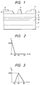
- Fig. 1 shows a high electron mobility transistor according to an embodiment of the present invention, in which the same parts as in the conventional device of Fig. 6 are represented by the same reference numerals and redundant descriptions therefor are omitted here.
- the main feature of this embodiment resides in that a first high-resistivity semiconductor channel layer 9 and a second high-resistivity semiconductor channel layer 10 are provided between the undoped semiconductor layer 2 and the doped semiconductor layer 3.
- the electron affinity of the first high-resistivity semiconductor channel layer 9 gradually increases toward the undoped semiconductor layer 2, and that of the second high-resistivity semiconductor layer 10 gradually decreases toward the undoped semiconductor layer 2.
- Each of the first and second high-resistivity semiconductor layers 9 and 10 has a composition of Al x In y Ga 1-x-y As, where x and y are determined, for example, as shown in Figs. 2 and 3.
- the ordinate of Fig. 2 represents a mole ratio of aluminum, i.e., x
- the ordinate of Fig. 3 represents a mole ratio of indium, i.e., y.
- the composition takes a form of Al x Ga 1-x As.
- it takes a form of In y Ga 1-y As, where the mole ratio of indium, i.e., y, is maximum at a position d2.
- the position d2 corresponds to the interface between the first and second high-resistivity semiconductor channel layers 9 and 10.
- the position d2 When added to GaAs, aluminum and indium serve to increase and decrease the potential, respectively. Therefore, as shown in an energy band diagram of Fig. 5(a), the position d2, where the mole ratio of indium is maximum, corresponds to the minimum position of a V-shaped portion.
- the overall energy band takes a form as shown in Figs. 4(a) when no voltage is applied to the gate electrode 4, and it becomes as shown in Fig. 4(b) when a negative voltage is applied.
- the center of gravity P of the electron distribution D does not vary.
- the device will have a superior electron controllability and low-noise characteristics.
- a generally V-shaped portion having a stepped variation may be provided as shown in Fig. 5(b). This is done by forming many layers having different compositions in each of the layers 9 and 10.
- the other layers may have the following compositions: undoped semiconductor layer 2, GaAs; doped semiconductor layer 3, n+-type AlGaAs; and cap layers 5, n+-type GaAs.
- the high electron mobility transistor having the above constitution, since the energy band structure in the electron accumulation layers assumes a generally symmetrical V shape, the center of gravity of the distribution of accumulated electrons does not move even if a negative voltage is applied to the gate electrode to raise the entire energy curve. As a result, the electron controllability and, therefore, noise characteristics can be improved.
- the energy curve is steeper on the side of the doped semiconductor layer 3. Therefore, when the gate voltage is changed, it is considered that the energy curve varies only on the side of the substrate 1 and the center of gravity of the electron distribution is moved thereby.
- First and second high-resistivity compound semiconductor channel layers are formed between an undoped compound semiconductor layer and a doped compound semiconductor layer having an electron affinity smaller than the undoped compound semiconductor layer.
- the first high-resistivity compound semiconductor channel layer is adjacent to the doped compound semiconductor layer, and has an electron affinity distribution that increases toward the undoped compound semiconductor layer.
- the second high-resistivity compound semiconductor channel layer is located between the first high-resistivity compound semiconductor channel layer and the undoped compound semiconductor layer, and has an electron affinity distribution that decreases toward the undoped compound semiconductor layer.
- a gate electrode and cap layers are formed on the doped compound semiconductor layer. Source and drain electrodes are formed on the respective cap layers.
Landscapes
- Junction Field-Effect Transistors (AREA)
Abstract
Description
- The present invention relates to compound semiconductor devices such as a HEMT (high electron mobility transistor).
- A HEMT structure is now drawing much attention, which is a field-effect transistor utilizing a two-dimensional electron gas accumulated in a heterojunction interface. The HEMT structure is illustrated in Fig. 6. An
undoped semiconductor layer 2 is formed on asubstrate 1, and adoped semiconductor layer 3 having an electron affinity smaller than thelayer 2 is formed on thelayer 2. Agate electrode 4 is formed on thedoped semiconductor layer 3. A source electrode 6 and adrain electrode 7 are formed oncap layers 5 that are formed on the doped semiconductor layer on both sides of thegate electrode 4. - In this HEMT structure, all the donor impurities added to the smaller electron affinity doped
semiconductor layer 3 are ionized, and electrons generated by this ionization are accumulated in the heterojunction interface with the larger electron affinityundoped semiconductor layer 2 to form a two-dimensional electron gas 8. The distribution of theelectron gas 8 can he controlled by a voltage applied to thegate electrode 4, to enable control of a current flowing between the source and drain. - Figs. 7(a) and 7(b) are energy band diagrams showing electron distributions D when no voltage is applied to the gate electrode 4 (Fig. 7(a)), i.e., the device is not in use, and when a certain negative voltage is applied (Fig. 7(b)). As shown in these figures, the distribution D of the two-
dimensional electron gas 8 assumes a mountain-like shape having some spread which is larger when the negative voltage is applied to thegate electrode 4. The degree of expansion depends on the magnitude of the negative voltage. - In other words, the center of gravity P of the electron distribution D goes farther away from the heterojunction interface as the negative voltage increases. Particularly in low-noise HEMTs in which a negative voltage is applied to the gate electrode to reduce the current, this phenomenon will deteriorate the electron controllability and make it difficult to realize satisfactory low-noise characteristics.
- The present invention has been made in view of the above problems in the art, and has an object of providing a high electron mobility transistor in which the center of gravity of the above-described electron distribution hardly moves.
- According to the invention, a high electron mobility transistor comprises:
undoped compound semiconductor layer;
doped compound semiconductor layer having an electron affinity smaller than the undoped compound semiconductor layer;
a gate electrode and a pair of cap layers formed on the doped compound semiconductor layer;
source and drain electrodes formed on the pair of cap layers, respectively;
a first high-resistivity compound semiconductor channel layer formed adjacent the doped compound semiconductor layer and having an electron affinity distribution that increases toward the undoped compound semiconductor layer; and
a second high-resistivity compound semiconductor channel layer formed between the first high-resistivity compound semiconductor channel layer and the undoped compound semiconductor layer and having an electron affinity distribution that decreases toward the undoped compound semiconductor layer. -
- Fig. 1 is a sectional view of a high electron mobility transistor according to an embodiment of the present invention;
- Figs. 2 and 3 show a variation of the composition of first and second high-resistivity semiconductor layers;
- Figs. 4(a) and 4(b) are energy band diagrams of the high electron mobility transistor according to the embodiment;
- Fig. 5(a) is an enlarged energy band diagram of a part of Fig. 4(a);
- Fig. 5(b) is an energy band diagram of a part of a high electron mobility transistor according to a modification;
- Fig. 6 is a sectional view of a conventional high electron mobility transistor; and
- Figs. 7(a) and 7(b) are energy band diagrams of the conventional high electron mobility transistor.
- Fig. 1 shows a high electron mobility transistor according to an embodiment of the present invention, in which the same parts as in the conventional device of Fig. 6 are represented by the same reference numerals and redundant descriptions therefor are omitted here. The main feature of this embodiment resides in that a first high-resistivity semiconductor channel layer 9 and a second high-resistivity
semiconductor channel layer 10 are provided between theundoped semiconductor layer 2 and thedoped semiconductor layer 3. The electron affinity of the first high-resistivity semiconductor channel layer 9 gradually increases toward theundoped semiconductor layer 2, and that of the second high-resistivity semiconductor layer 10 gradually decreases toward theundoped semiconductor layer 2. - Each of the first and second high-
resistivity semiconductor layers 9 and 10 has a composition of AlxInyGa1-x-yAs, where x and y are determined, for example, as shown in Figs. 2 and 3. In Figs. 2 and 3, symbol d represents a position in the thickness direction of the first and second high-resistivitysemiconductor channel layers 9 and 10, where d = 0 corresponds to the interface with thedoped semiconductor layer 3 and d = d3 corresponds to the interface with theundoped semiconductor layer 2. - The ordinate of Fig. 2 represents a mole ratio of aluminum, i.e., x, and the ordinate of Fig. 3 represents a mole ratio of indium, i.e., y. In the range of 0-d1, the composition takes a form of AlxGa1-xAs. In the range of d1-d3, it takes a form of InyGa1-yAs, where the mole ratio of indium, i.e., y, is maximum at a position d2. The position d2 corresponds to the interface between the first and second high-resistivity
semiconductor channel layers 9 and 10. When added to GaAs, aluminum and indium serve to increase and decrease the potential, respectively. Therefore, as shown in an energy band diagram of Fig. 5(a), the position d2, where the mole ratio of indium is maximum, corresponds to the minimum position of a V-shaped portion. - By providing the first and second high-resistivity
semiconductor channel layers 9 and 10 in the above manner, the overall energy band takes a form as shown in Figs. 4(a) when no voltage is applied to thegate electrode 4, and it becomes as shown in Fig. 4(b) when a negative voltage is applied. As is understood from Figs. 4(a) and 4(b), the center of gravity P of the electron distribution D does not vary. As a result, when put into actual use, the device will have a superior electron controllability and low-noise characteristics. - If it is difficult to produce the high-resistivity
semiconductor channel layers 9 and 10 each having the continuous variation of the electron affinity, a generally V-shaped portion having a stepped variation may be provided as shown in Fig. 5(b). This is done by forming many layers having different compositions in each of thelayers 9 and 10. - In Fig. 1, the other layers may have the following compositions: undoped
semiconductor layer 2, GaAs; dopedsemiconductor layer 3, n⁺-type AlGaAs; andcap layers 5, n⁺-type GaAs. - According to the high electron mobility transistor having the above constitution, since the energy band structure in the electron accumulation layers assumes a generally symmetrical V shape, the center of gravity of the distribution of accumulated electrons does not move even if a negative voltage is applied to the gate electrode to raise the entire energy curve. As a result, the electron controllability and, therefore, noise characteristics can be improved. On the other hand, in the conventional device, the energy curve is steeper on the side of the
doped semiconductor layer 3. Therefore, when the gate voltage is changed, it is considered that the energy curve varies only on the side of thesubstrate 1 and the center of gravity of the electron distribution is moved thereby. - First and second high-resistivity compound semiconductor channel layers are formed between an undoped compound semiconductor layer and a doped compound semiconductor layer having an electron affinity smaller than the undoped compound semiconductor layer. The first high-resistivity compound semiconductor channel layer is adjacent to the doped compound semiconductor layer, and has an electron affinity distribution that increases toward the undoped compound semiconductor layer. The second high-resistivity compound semiconductor channel layer is located between the first high-resistivity compound semiconductor channel layer and the undoped compound semiconductor layer, and has an electron affinity distribution that decreases toward the undoped compound semiconductor layer. A gate electrode and cap layers are formed on the doped compound semiconductor layer. Source and drain electrodes are formed on the respective cap layers.
Claims (3)
- A high electron mobility transistor comprising:
undoped compound semiconductor layer;
doped compound semiconductor layer having an electron affinity smaller than the undoped compound semiconductor layer;
a gate electrode and a pair of cap layers formed on the doped compound semiconductor layer;
source and drain electrodes formed on the pair of cap layers, respectively;
a first high-resistivity compound semiconductor channel layer formed adjacent the doped compound semiconductor layer and having an electron affinity distribution that increases toward the undoped compound semiconductor layer; and
a second high-resistivity compound semiconductor channel layer formed between the first high-resistivity compound semiconductor channel layer and the undoped compound semiconductor layer and having an electron affinity distribution that decreases toward the undoped compound semiconductor layer. - The high electron mobility transistor of claim 1, wherein the electron affinity distributions of the first and second high-resistivity compound semiconductor channel layers are step-like distributions.
- The high electron mobility transistor of claim 1, wherein the first and second high-resistivity compound semiconductor channel layers have a composition of AlxInyGa1-x-yAs, where x monotonously decreases to zero in the first high-resistivity compound semiconductor channel layer and y takes a maximum at a boundary between the first and second high-resistivity compound semiconductor channel layers.
Applications Claiming Priority (2)
| Application Number | Priority Date | Filing Date | Title |
|---|---|---|---|
| JP3311826A JPH05121453A (en) | 1991-10-29 | 1991-10-29 | Compound semiconductor device |
| JP311826/91 | 1991-10-29 |
Publications (3)
| Publication Number | Publication Date |
|---|---|
| EP0539949A2 true EP0539949A2 (en) | 1993-05-05 |
| EP0539949A3 EP0539949A3 (en) | 1994-02-02 |
| EP0539949B1 EP0539949B1 (en) | 1996-03-06 |
Family
ID=18021868
Family Applications (1)
| Application Number | Title | Priority Date | Filing Date |
|---|---|---|---|
| EP92118429A Expired - Lifetime EP0539949B1 (en) | 1991-10-29 | 1992-10-28 | High electron mobility transistor having improved electron controllability |
Country Status (5)
| Country | Link |
|---|---|
| US (1) | US5412230A (en) |
| EP (1) | EP0539949B1 (en) |
| JP (1) | JPH05121453A (en) |
| CA (1) | CA2080081C (en) |
| DE (1) | DE69208808T2 (en) |
Families Citing this family (2)
| Publication number | Priority date | Publication date | Assignee | Title |
|---|---|---|---|---|
| JPH0815213B2 (en) * | 1993-01-14 | 1996-02-14 | 日本電気株式会社 | Field effect transistor |
| JP3421306B2 (en) | 2000-07-19 | 2003-06-30 | 富士通カンタムデバイス株式会社 | Compound semiconductor device |
Family Cites Families (6)
| Publication number | Priority date | Publication date | Assignee | Title |
|---|---|---|---|---|
| JPS6328072A (en) * | 1986-07-21 | 1988-02-05 | Sumitomo Electric Ind Ltd | Field effect transistor |
| JPS6414972A (en) * | 1987-07-08 | 1989-01-19 | Nec Corp | Field-effect transistor |
| JPS6431470A (en) * | 1987-07-27 | 1989-02-01 | Nec Corp | Field effect transistor |
| JPH02202029A (en) * | 1989-01-31 | 1990-08-10 | Sony Corp | Compound semiconductor device |
| JPH03224243A (en) * | 1989-12-26 | 1991-10-03 | Sanyo Electric Co Ltd | Velocity modulation transistor |
| US5206527A (en) * | 1990-11-09 | 1993-04-27 | Sumitomo Electric Industries, Ltd. | Field effect transistor |
-
1991
- 1991-10-29 JP JP3311826A patent/JPH05121453A/en active Pending
-
1992
- 1992-09-30 US US07/954,909 patent/US5412230A/en not_active Expired - Lifetime
- 1992-10-07 CA CA002080081A patent/CA2080081C/en not_active Expired - Fee Related
- 1992-10-28 EP EP92118429A patent/EP0539949B1/en not_active Expired - Lifetime
- 1992-10-28 DE DE69208808T patent/DE69208808T2/en not_active Expired - Fee Related
Also Published As
| Publication number | Publication date |
|---|---|
| CA2080081C (en) | 1997-05-20 |
| CA2080081A1 (en) | 1993-04-30 |
| EP0539949A3 (en) | 1994-02-02 |
| EP0539949B1 (en) | 1996-03-06 |
| JPH05121453A (en) | 1993-05-18 |
| DE69208808D1 (en) | 1996-04-11 |
| DE69208808T2 (en) | 1996-08-08 |
| US5412230A (en) | 1995-05-02 |
Similar Documents
| Publication | Publication Date | Title |
|---|---|---|
| US4916498A (en) | High electron mobility power transistor | |
| US4984036A (en) | Field effect transistor with multiple grooves | |
| US7800131B2 (en) | Field effect transistor | |
| US7863648B2 (en) | Field effect transistor | |
| US6586813B2 (en) | High-speed compound semiconductor device operable at large output power with minimum leakage current | |
| US5285087A (en) | Heterojunction field effect transistor | |
| US7388235B2 (en) | High electron mobility transistors with Sb-based channels | |
| US5023674A (en) | Field effect transistor | |
| EP0514079B1 (en) | High electron mobility transistor and method of manufacture | |
| US10879368B2 (en) | Transistor with multi-metal gate | |
| US5105241A (en) | Field effect transistor | |
| JP2661555B2 (en) | Heterojunction field effect transistor | |
| JPH11261051A (en) | Semiconductor device | |
| KR19990077669A (en) | Field effect transistor | |
| JP3058262B2 (en) | Heterojunction field effect transistor | |
| US5448086A (en) | Field effect transistor | |
| US5473175A (en) | Multi-2DEG HEMT | |
| US4967242A (en) | Heterojunction field effect transistor | |
| JPH0645366A (en) | Field effect transistor | |
| JP2005159117A (en) | Nitride semiconductor devices | |
| US5412230A (en) | High electron mobility transistor having improved electron controllability | |
| WO2001057914A2 (en) | Process of manufacturing a semiconductor device including a buried channel field effect transistor | |
| US6049097A (en) | Reliable HEMT with small parasitic resistance | |
| US7173292B2 (en) | Field effect transistor | |
| JP2005191449A (en) | Field effect transistor |
Legal Events
| Date | Code | Title | Description |
|---|---|---|---|
| PUAI | Public reference made under article 153(3) epc to a published international application that has entered the european phase |
Free format text: ORIGINAL CODE: 0009012 |
|
| AK | Designated contracting states |
Kind code of ref document: A2 Designated state(s): DE FR GB |
|
| PUAL | Search report despatched |
Free format text: ORIGINAL CODE: 0009013 |
|
| AK | Designated contracting states |
Kind code of ref document: A3 Designated state(s): DE FR GB |
|
| 17P | Request for examination filed |
Effective date: 19940727 |
|
| 17Q | First examination report despatched |
Effective date: 19950322 |
|
| GRAA | (expected) grant |
Free format text: ORIGINAL CODE: 0009210 |
|
| AK | Designated contracting states |
Kind code of ref document: B1 Designated state(s): DE FR GB |
|
| REF | Corresponds to: |
Ref document number: 69208808 Country of ref document: DE Date of ref document: 19960411 |
|
| ET | Fr: translation filed | ||
| GRAH | Despatch of communication of intention to grant a patent |
Free format text: ORIGINAL CODE: EPIDOS IGRA |
|
| PLBE | No opposition filed within time limit |
Free format text: ORIGINAL CODE: 0009261 |
|
| STAA | Information on the status of an ep patent application or granted ep patent |
Free format text: STATUS: NO OPPOSITION FILED WITHIN TIME LIMIT |
|
| 26N | No opposition filed | ||
| PGFP | Annual fee paid to national office [announced via postgrant information from national office to epo] |
Ref country code: FR Payment date: 20011010 Year of fee payment: 10 |
|
| PGFP | Annual fee paid to national office [announced via postgrant information from national office to epo] |
Ref country code: GB Payment date: 20011031 Year of fee payment: 10 |
|
| PGFP | Annual fee paid to national office [announced via postgrant information from national office to epo] |
Ref country code: DE Payment date: 20011112 Year of fee payment: 10 |
|
| REG | Reference to a national code |
Ref country code: GB Ref legal event code: IF02 |
|
| PG25 | Lapsed in a contracting state [announced via postgrant information from national office to epo] |
Ref country code: GB Free format text: LAPSE BECAUSE OF NON-PAYMENT OF DUE FEES Effective date: 20021028 |
|
| PG25 | Lapsed in a contracting state [announced via postgrant information from national office to epo] |
Ref country code: DE Free format text: LAPSE BECAUSE OF NON-PAYMENT OF DUE FEES Effective date: 20030501 |
|
| GBPC | Gb: european patent ceased through non-payment of renewal fee | ||
| PG25 | Lapsed in a contracting state [announced via postgrant information from national office to epo] |
Ref country code: FR Free format text: LAPSE BECAUSE OF NON-PAYMENT OF DUE FEES Effective date: 20030630 |
|
| REG | Reference to a national code |
Ref country code: FR Ref legal event code: ST |