EP0538902B1 - Image forming apparatus having recording material separating means - Google Patents
Image forming apparatus having recording material separating means Download PDFInfo
- Publication number
- EP0538902B1 EP0538902B1 EP92118261A EP92118261A EP0538902B1 EP 0538902 B1 EP0538902 B1 EP 0538902B1 EP 92118261 A EP92118261 A EP 92118261A EP 92118261 A EP92118261 A EP 92118261A EP 0538902 B1 EP0538902 B1 EP 0538902B1
- Authority
- EP
- European Patent Office
- Prior art keywords
- recording material
- separation
- image
- voltage
- transfer
- Prior art date
- Legal status (The legal status is an assumption and is not a legal conclusion. Google has not performed a legal analysis and makes no representation as to the accuracy of the status listed.)
- Expired - Lifetime
Links
Images


Classifications
-
- G—PHYSICS
- G03—PHOTOGRAPHY; CINEMATOGRAPHY; ANALOGOUS TECHNIQUES USING WAVES OTHER THAN OPTICAL WAVES; ELECTROGRAPHY; HOLOGRAPHY
- G03G—ELECTROGRAPHY; ELECTROPHOTOGRAPHY; MAGNETOGRAPHY
- G03G15/00—Apparatus for electrographic processes using a charge pattern
- G03G15/65—Apparatus which relate to the handling of copy material
- G03G15/6532—Removing a copy sheet form a xerographic drum, band or plate
- G03G15/6535—Removing a copy sheet form a xerographic drum, band or plate using electrostatic means, e.g. a separating corona
-
- B—PERFORMING OPERATIONS; TRANSPORTING
- B82—NANOTECHNOLOGY
- B82Y—SPECIFIC USES OR APPLICATIONS OF NANOSTRUCTURES; MEASUREMENT OR ANALYSIS OF NANOSTRUCTURES; MANUFACTURE OR TREATMENT OF NANOSTRUCTURES
- B82Y15/00—Nanotechnology for interacting, sensing or actuating, e.g. quantum dots as markers in protein assays or molecular motors
Definitions
- the present invention relates to an image forming apparatus such as an electrophotographic apparatus or electrostatic recording apparatus, which is provided with separating means for electrostatically separating a recording material.
- An electrostatic separating means has been proposed as a transfer material separating means, in which a separating charger is disposed at a predetermined position immediately after the image transfer position to apply electric charge having the polarity opposite to that of the transfer charger to the transfer material to neutralize or discharge the electric charge applied during the transfer operation, by which the attraction force toward the image bearing member is reduced.
- This electrostatic separation means is effective to a certain extent.
- the separation charger is in the form of an AC corona discharger supplied with a DC biased AC voltage, and is called electrostatic separation system.
- FIG. 6 there is shown an electrostatic separation system, schematically.
- a transfer charger 2 Adjacent the position where the transfer material P is contacted to the toner image T (charged to the negative polarity) on the image bearing member in the form of a photosensitive drum 1, a transfer charger 2 supplies to the backside of the transfer material P a transfer potential having the polarity (positive) opposite to that of the toner image T, so that the toner image T is transferred onto the transfer material P.
- an AC discharge operation is effected by a separation charger 3 for removing the transfer potential.
- the recent increase of the copy speed is remarkable with the result that it becomes difficult to maintain the transfer and separation performance by increasing the peak-to-peak voltage Vpp alone. More particularly, if the peak-to-peak voltage Vpp is too high, the toner image T may be deposited back to the photosensitive drum 1 during the separating action (back-transfer).
- the problem is particularly remarkable in the case of high speed copying machines in which the transfer material feeding speed is not less than about 300 mm/sec.
- the problem is not remarkable in middle or low speed machines, but assisting mechanisms such as pre-transfer charger, pre-transfer exposure, air sucking (separation pawls, separation belt, scorotron separation charger or the like), in order to prevent the back-transfer.
- assisting mechanisms such as pre-transfer charger, pre-transfer exposure, air sucking (separation pawls, separation belt, scorotron separation charger or the like), in order to prevent the back-transfer.
- the disadvantages of high cost and poor durability are involved.
- a current difference which is a difference between an absolute value of the positive component and the absolute value of the negative component in the separation charger, is adjusted to provide a desired separation performance. If the current difference is directed strongly to the side of the same polarity as the transfer bias, an improper separation action occurs due to insufficient electric discharge of the transfer material. If it is strongly directed to the side of the polarity opposite to that of the transfer bias, the back-transfer is liable to occur due to excessive discharge. In order to effect stabilized separation, it is desirable that the proper current range of the current difference is large. In order to achieve this, Japanese Laid-Open Patent Application No.
- US 4 979 000 discloses an image forming apparatus for forming an image on a recording sheet comprising a photosensitive drum for holding a toner image thereon, a developer for forming the toner image on the photosensitive drum, an image transfer device for electrostatically transferring the toner image from the photosensitive drum to the recording sheet and a sheet seperator for separating the recording sheet from the photosensitive drum as the recording sheet advances.
- the sheet separator comprises a single fork-like electrode and is controlled to generate a discharge voltage which includes at least alternating currents at various duty factors.
- Figure 1 is a schematic sectional view of an image forming apparatus according to an embodiment of the present invention.
- Figure 2 is a graph showing a relationship between a transfer material conveying speed and a total discharging current.
- Figure 3 is a side view of a transfer material separating device in an image forming apparatus according to a second embodiment of the present invention.
- Figure 4 is a side view of a separation charger which is a modification of the separation charger of Figure 3.
- Figure 5 is a side view of a transfer material separating device used in an image forming apparatus according to a third embodiment of the present invention.
- Figure 6 is a side view of a transfer material separating device not using the present invention.
- Figure 7 is a graph of discharging current through a photosensitive drum.
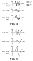
- Figure 8 is graphs of discharging currents through a point Q before a separation point.
- Figure 9 is graphs of potential change corresponding to (1), (2) and (3) of Figure 8.
- Figure 10 is a graph showing a relationship between a change of current difference and a backside potential of the transfer material after the separation.
- Figure 11 is a side view of an opening of a separation charger with a grid.
- Figures 12 and 13 are side views of shields of separation chargers according to other examples.
- an image forming apparatus there is shown an image forming apparatus according to an embodiment of the present invention.
- the photosensitive drum 1 comprises an amorphous silicon photosensitive layer 1A having a positive charging property and a conductive base electrically grounded and effective to support the photosensitive layer 1A.
- the photosensitive drum 1 is electrically charged to the positive polarity by a charger 7, and is exposed to image light L in accordance with image information representing original or the like, so that an electrostatic latent image is formed.
- the electrostatic latent image is developed by a developing device 8 with the toner particles charged to the negative polarity.
- the toner image T is developed and is transferred from the photosensitive drum 1 onto the recording material in the form of a transfer material P (paper or the like) by a transfer corona charger 2.
- the charger 2 is supplied with a voltage of the positive polarity which is the opposite from the charging polarity of the toner.
- the charger 2 supplies positive electric charge to the backside of the transfer material P.
- a separation corona charger 3 removes the transfer charge from the backside of the transfer material P, thus diminishing the electrostatic attraction force between the photosensitive drum 1 and the transfer material P, so that the transfer material P is permitted to be separated from the photosensitive drum 1.
- the separation corona charger 3 comprises a wire electrode 31 and a shield electrode 32.
- the wire electrodes 31 is supplied with a DC biased AC voltage, in which the DC component has a negative polarity which is the opposite from the transfer charge polarity.
- the transfer material carrying the toner image T is conveyed to an image fixing device 10, so that a toner image T is fixed on the transfer material P.
- the photosensitive drum 1 is cleaned by a cleaner 7 so that the residual toner is removed therefrom. Thereafter, the photosensitive drum 1 is uniformly exposed to light by an unshown pre-exposure lamp, so that the residual electric charge is removed to be prepared for the repeated image forming operation.
- a transfer charger 2' is supplied with a voltage having a polarity opposite from that of the charging polarity of the toner image T', and the separation charger 3' is supplied with a DC biased AC voltage in which the DC component has the polarity opposite from that of the transfer voltage.
- Figure 7 is a graph of the discharge current through the photosensitive drum from the transfer charger 2' and the separation charger 3' in Figure 6. After the photosensitive drum 1 is subjected to the transfer discharge current having the polarity (positive) opposite from that of the toner, it is subjected to the AC discharge current for the electric discharge. Figure 7 shows that the separation point A of the transfer material P from the photosensitive drum 1 is a point where the photosensitive drum 1 and the discharging wire electrode 31' of the separation charger 3' are closest, that is, where the discharge current from the separation charger 3' is largest. The separation at this point is most stable, since the received discharging current decreases, and therefore, the separation power decreases, after the point A.
- (1) shows the AC discharge current Ip received from the separation charger with respect to a movement distance x of a point Q on the transfer material before the separation point A; (2) shows the same when the transfer material conveying speed Vp is doubled in which the period of the current Ip is twice, and the peak level of the current Ip is one half. Therefore, the total current received by the point Q before it reaches the point A, (
- (3) shows the case in which the voltage Vpp is increased so that the discharge current (
- a current difference Is which is the difference between the absolute value of a positive component of the separation discharge current and the absolute value of the negative component thereof, is adjusted to provide a desired separation function.
- the proper range may change or reduce due the ambient conditions or copy modes. Therefore, in order to provide the stabilized separation at all times, it is desirable to increase the range.
- the separation charger 3 is disposed faced to the photosensitive member 1, and the opening of the shield of the separation charger 3 is reduced toward the photosensitive member 1, as shown in Figure 1.
- the opening 32A is smaller than the shield bottom 32B.
- Figures 12 and 13 show other examples satisfying this requirement.
- the current tends to leak to the edge 32C of the shield 32 with the result of the tendency of the toner particles and the paper dust being attracted to the edge 32C.
- Figure 1 and Figure 13 configurations are preferable in which the shield edge 32C is gradually away from the discharging electrode 31 comprising a wire.
- the discharge current into the shield is not less than 60 % of the total discharge current.
- the discharge current into the reducing portion of the shield is not less than 10 % of the total discharging current. The percentages can be controlled by properly selecting the distances between the wire electrode and the portions of the inside surface of the shield.
- the transfer action is assured by increasing the frequency f of the separation AC voltage. This will be described in detail.
- Table 1 shows whether the range is practically usable or not.
- Table 1 three right side data with the frequencies given, are for the case of using the separation charger in which the shield opening is not reduced.
- the leftmost data are for the separation charger having the reduced opening as shown in Figure 1 with the frequency of 500 Hz.
- the proper current difference range reduces very much if the transfer material conveying speed Vp > 300 mm/sec. For this reason, if the electrophotographic apparatus has a photosensitive drum and has a process speed Vp which is higher than 300 mm/sec, the above-described assisting device or devices (pre-transfer charger or the like) have to be used between the developing device and the transfer charger in most cases.
- the performance is further improved if the frequency of the separation high voltage is increased to 1000 Hz.
- the performance is stabilized by the improvement of the charger, and the performance can be increased very much by the increase of the frequency.
- Table 2 shows the results of the investigated proper current difference range for the various conveying speed Vp when the opening is reduced as shown in Figure 1, and the frequency of the AC separating high voltage is increased.
- Vp/f in the parentheses are spatial periods on the transfer material corresponding to the time periods of the separation AC high voltage.
- the frequency f may be adjusted if necessary. In the transfer material separating device of this embodiment, when the transfer material conveying speed Vp is not less than 300 mm/sec, the frequency f is increased up to 600 - 1400 Hz, and the opening is reduced or converged.
- the toner image T provided by the development is charged to the negative polarity, and is attracted by the positive electric charge of the image on the photosensitive member 1.
- the transfer charger 2 providing the positive corona discharge
- the backside of the transfer material P is charged to the positive polarity, which is effective to attract the toner image T onto the transfer material.
- the transfer material P proceeds toward the separation charger 3
- the backside of the transfer material is electrically discharged by AC corona discharge.
- the transfer material P with the toner image T is separated from the drum 1 by the rigidity of the transfer material P, and it is conveyed to an image fixing device, and is discharged to the outside of the apparatus.
- the separation charging means 3 comprises a first separation charger 31 and a second separation charger 32 to stabilize the separating performance.
- the total current from the transformer is doubled, and the discharging region is doubled.
- the next separation charger 32 is effective to further discharge it. Therefore, the risk of the paper jam due to the paper or transfer material P wrapping around the photosensitive drum 1, can be remarkably reduced.
- Figure 4 shows an embodiment in which the frequency of the AC voltage applied to the discharging wire electrode 31a and the frequency of the AC voltage applied to the discharging wire electrode 31b which is downstream with respect to the movement direction of the transfer material, are made different.
- the transfer material conveying speed Vp is approximately 400 mm/sec
- the AC high voltage supplied to the separation charger is not less than 10 KVpp
- two discharging electrodes require total transformer output current (
- the used frequency is preferably not less than 800 - 1000 Hz, which, however, may be hard by people as corona noise in 3 case.
- the upstream discharging electrode 31a is more effective in the separating power and the back-transfer transfer prevention than the downstream one, and the downstream one has an auxiliary effect. Therefore, the voltage applied to the upstream wire electrode is given a higher frequency than the downstream one.
- the downstream wire electrode 31b is supplied with a voltage having such a low frequency which is lower than the audible range, by which the volume of the audible range can be decreased. By doing so, the noise level is substantially equivalent to the case of single separation discharging electrode.
- the reduced opening structure of the shield may be usable for both of the upstream and downstream separation dischargers, by which the contamination can be prevented in both of the chargers.
- the reduced opening structure of the shield may be used only in the upstream one, as shown in Figure 4, if desirable.
- the separation charger is used to separate the recording material from the image bearing member.
- the present invention is not limited to such use.
- Figure 5 is a side view of a major portion of an image forming apparatus using the separating device of Figure 1.
- a transfer belt 5 is trained around transfer belt supporting rollers 4a, 4b and 4c.
- the roller 4a is a conductive roller which is electrically grounded.
- a transfer member 20 for applying a transfer bias so as to face the photosensitive member 1.
- the transfer belt 5 is made of dielectric material having a volume resistivity of approximately 10 14 ohm.cm and has a thickness of approximately 50 microns. It rotates in the direction indicated by an arrow D in synchronism with the photosensitive member 1.
- the transfer material P is supplied from the left of the transfer belt to the transfer position, where it is supplied with the transfer bias by the transfer member 20.
- the transfer bias voltage is -3 KV, for example, which constitutes an electric field.
- the toner image electrostatically formed on the surface of the photosensitive member 1 is transferred onto the transfer material P.
- the toner image is formed in the same manner as in the case of Figure 1.
- the transfer material P is kept attracted on the transfer belt 5 electrically charged by the transfer member 6, and is conveyed to the right to the separating position C, where it is separated from the transfer belt 2 and is conveyed to an unshown image fixing station.
- the residual charge on the transfer belt is dissipated by the time it reaches the position where the transfer material is separated from the transfer belt, and therefore, no special discharging means is required.
- a separation charger 3 for effecting high frequency AC discharge (800 Hz) to a separating position C is disposed at the separating position C.
- the structure of the separation charger is the same as in Figure 1.
- the waveform of the AC voltage may be sine, triangular, rectangular or the like.
- the AC voltage may be in the form of the rectangular provided by periodically rendering on and off a AC voltage source, and various voltage which changes periodically is usable.
- the frequency of the AC voltage applied to the separation charger is increased in accordance with the conveying speed of the recording material, and the opening of the shield electrode is reduced, by which the improper separation, the back transfer, the image defects due to the separation discharge or the like, can be avoided with stability and with high durability.
Description
- The present invention relates to an image forming apparatus such as an electrophotographic apparatus or electrostatic recording apparatus, which is provided with separating means for electrostatically separating a recording material.
- In a known image forming apparatus in which a transferable toner image is formed on a surface of an image bearing member such as a photosensitive member and a dielectric member, is electrostatically transferred onto a transfer material or recording material in the form of paper or sheet, the electric charge applied to the transfer material during the transfer operation results in the tendency, after the image transfer operation, that the transfer material is attracted electrostatically to the image bearing member. Therefore some separating means is used to positively separate the transfer material from the image bearing member.
- An electrostatic separating means has been proposed as a transfer material separating means, in which a separating charger is disposed at a predetermined position immediately after the image transfer position to apply electric charge having the polarity opposite to that of the transfer charger to the transfer material to neutralize or discharge the electric charge applied during the transfer operation, by which the attraction force toward the image bearing member is reduced. This electrostatic separation means is effective to a certain extent.
- Generally, the separation charger is in the form of an AC corona discharger supplied with a DC biased AC voltage, and is called electrostatic separation system.
- Referring first to Figure 6, there is shown an electrostatic separation system, schematically. Adjacent the position where the transfer material P is contacted to the toner image T (charged to the negative polarity) on the image bearing member in the form of a
photosensitive drum 1, atransfer charger 2 supplies to the backside of the transfer material P a transfer potential having the polarity (positive) opposite to that of the toner image T, so that the toner image T is transferred onto the transfer material P. Subsequently, in order to separate the transfer material P from thephotosensitive drum 1 with the toner image T, an AC discharge operation is effected by aseparation charger 3 for removing the transfer potential. - When the transfer material carrying speed Vp is increased in response to increase of the copy speed, the removal of the transfer potential becomes insufficient with the result of improper separation. In view of this, it will be considered that the peak-to-peak voltage Vpp of the AC voltage applied to the separation charger is increased.
- However, the recent increase of the copy speed is remarkable with the result that it becomes difficult to maintain the transfer and separation performance by increasing the peak-to-peak voltage Vpp alone. More particularly, if the peak-to-peak voltage Vpp is too high, the toner image T may be deposited back to the
photosensitive drum 1 during the separating action (back-transfer). - The problem is particularly remarkable in the case of high speed copying machines in which the transfer material feeding speed is not less than about 300 mm/sec. The problem is not remarkable in middle or low speed machines, but assisting mechanisms such as pre-transfer charger, pre-transfer exposure, air sucking (separation pawls, separation belt, scorotron separation charger or the like), in order to prevent the back-transfer. In any case, the disadvantages of high cost and poor durability, are involved.
- On the other hand, it is general that a current difference which is a difference between an absolute value of the positive component and the absolute value of the negative component in the separation charger, is adjusted to provide a desired separation performance. If the current difference is directed strongly to the side of the same polarity as the transfer bias, an improper separation action occurs due to insufficient electric discharge of the transfer material. If it is strongly directed to the side of the polarity opposite to that of the transfer bias, the back-transfer is liable to occur due to excessive discharge. In order to effect stabilized separation, it is desirable that the proper current range of the current difference is large. In order to achieve this, Japanese Laid-Open Patent Application No. 9375/1987 proposes that an opening of a shield of the separation charger is provided with a grid electrically connected to an impedance element Z in an attempt to provide the above-described effect (Figure 11). However, in long term use, the grid is contaminated with toner particles and paper dust, so that the expected function is not performed (after 200,000 - 300,000 sheets). In addition, the grid has a limited service life (it becomes easily broken after 500,000 sheets are processed), and therefore, the durability is not high.
- As will be understood from the foregoing, the increase of the transfer material conveying speed Vp results in the improper separation or transfer-back, and the use of the grid in the opening of the separating charger involves in sufficient durability.
- US 4 979 000 discloses an image forming apparatus for forming an image on a recording sheet comprising a photosensitive drum for holding a toner image thereon, a developer for forming the toner image on the photosensitive drum, an image transfer device for electrostatically transferring the toner image from the photosensitive drum to the recording sheet and a sheet seperator for separating the recording sheet from the photosensitive drum as the recording sheet advances. The sheet separator comprises a single fork-like electrode and is controlled to generate a discharge voltage which includes at least alternating currents at various duty factors.
- Accordingly, it is a principal object of the present invention to provide an image forming apparatus in which the improper separation or the back-transfer are effectively prevented.
- It is another object of the present invention to provide an image forming apparatus having high durability.
- It is a further object of the present invention to provide an image forming apparatus in which good separation is possible even if the recording material conveying speed is increased.
- It is a further object of the present invention to provide an image forming apparatus in which durability of a grid electrode disposed in an opening of a shield of a separation discharger, can be increased.
- These objects are achieved by image forming apparatusses having the features of
claim 1 or 7. The invention is further developed by the features mentioned in the dependent claims. - Figure 1 is a schematic sectional view of an image forming apparatus according to an embodiment of the present invention.
- Figure 2 is a graph showing a relationship between a transfer material conveying speed and a total discharging current.
- Figure 3 is a side view of a transfer material separating device in an image forming apparatus according to a second embodiment of the present invention.
- Figure 4 is a side view of a separation charger which is a modification of the separation charger of Figure 3.
- Figure 5 is a side view of a transfer material separating device used in an image forming apparatus according to a third embodiment of the present invention.
- Figure 6 is a side view of a transfer material separating device not using the present invention.
- Figure 7 is a graph of discharging current through a photosensitive drum.
- Figure 8 is graphs of discharging currents through a point Q before a separation point.
- Figure 9 is graphs of potential change corresponding to (1), (2) and (3) of Figure 8.
- Figure 10 is a graph showing a relationship between a change of current difference and a backside potential of the transfer material after the separation.
- Figure 11 is a side view of an opening of a separation charger with a grid.
- Figures 12 and 13 are side views of shields of separation chargers according to other examples.
- Referring to the accompanying drawings, the description will be made as to the embodiments of the present invention.
- Referring to Figure 1, there is shown an image forming apparatus according to an embodiment of the present invention. In this Figure, an image bearing member in the form of a
photosensitive drum 1 is rotated in a direction indicated by an arrow A at a predetermined peripheral speed (= Vp mm/sec). In this embodiment, thephotosensitive drum 1 comprises an amorphous silicon photosensitive layer 1A having a positive charging property and a conductive base electrically grounded and effective to support the photosensitive layer 1A. Thephotosensitive drum 1 is electrically charged to the positive polarity by a charger 7, and is exposed to image light L in accordance with image information representing original or the like, so that an electrostatic latent image is formed. The electrostatic latent image is developed by a developingdevice 8 with the toner particles charged to the negative polarity. The toner image T is developed and is transferred from thephotosensitive drum 1 onto the recording material in the form of a transfer material P (paper or the like) by atransfer corona charger 2. At this time, thecharger 2 is supplied with a voltage of the positive polarity which is the opposite from the charging polarity of the toner. Thecharger 2 supplies positive electric charge to the backside of the transfer material P. After the image transfer, aseparation corona charger 3 removes the transfer charge from the backside of the transfer material P, thus diminishing the electrostatic attraction force between thephotosensitive drum 1 and the transfer material P, so that the transfer material P is permitted to be separated from thephotosensitive drum 1. Theseparation corona charger 3 comprises awire electrode 31 and ashield electrode 32. Thewire electrodes 31 is supplied with a DC biased AC voltage, in which the DC component has a negative polarity which is the opposite from the transfer charge polarity. - The transfer material carrying the toner image T is conveyed to an
image fixing device 10, so that a toner image T is fixed on the transfer material P. - On the other hand, after the image transfer, the
photosensitive drum 1 is cleaned by a cleaner 7 so that the residual toner is removed therefrom. Thereafter, thephotosensitive drum 1 is uniformly exposed to light by an unshown pre-exposure lamp, so that the residual electric charge is removed to be prepared for the repeated image forming operation. - Referring to Figure 6, the description will be made as to the case of a separation charger 3' shown in Figure 6 which has a shield having a configuration which is different from that of Figure 1 separation charger. In Figure 6, a transfer charger 2' is supplied with a voltage having a polarity opposite from that of the charging polarity of the toner image T', and the separation charger 3' is supplied with a DC biased AC voltage in which the DC component has the polarity opposite from that of the transfer voltage.
- Figure 7 is a graph of the discharge current through the photosensitive drum from the transfer charger 2' and the separation charger 3' in Figure 6. After the
photosensitive drum 1 is subjected to the transfer discharge current having the polarity (positive) opposite from that of the toner, it is subjected to the AC discharge current for the electric discharge. Figure 7 shows that the separation point A of the transfer material P from thephotosensitive drum 1 is a point where thephotosensitive drum 1 and the discharging wire electrode 31' of the separation charger 3' are closest, that is, where the discharge current from the separation charger 3' is largest. The separation at this point is most stable, since the received discharging current decreases, and therefore, the separation power decreases, after the point A. - If the copying speed is increased, and therefore, the transfer material conveying speed Vp is increased, the transfer potential is not sufficiently removed with the result of increase of liability of improper separation. In view of this, it would be considered that the peak-to-peak voltage to the separation charger is increased. However, if it is too large, the toner image may be transfers back to the photosensitive drum 1 (back-transfer).
- Referring to Figure 8, this will be described in more detail. In Figure 8, (1) shows the AC discharge current Ip received from the separation charger with respect to a movement distance x of a point Q on the transfer material before the separation point A; (2) shows the same when the transfer material conveying speed Vp is doubled in which the period of the current Ip is twice, and the peak level of the current Ip is one half. Therefore, the total current received by the point Q before it reaches the point A, (|Ip+| + |Ip-|) is one half with the result of the liability of separation failure before the point A. In Figure 8, (3) shows the case in which the voltage Vpp is increased so that the discharge current (|Ip+| + |Ip-|) is the same as in the case (1). By doing so, the separation power becomes equivalent to that of the case (1).
- The change of the potential of the transfer material P having received the current Ip of Figure 8, is shown in Figure 9. Since it corresponds to an integration of ¦Ip¦, and therefore, in the case of (3), the peak potential reaches twice the peak potential of the case (1). As a result, the back-transfer becomes liable when the Vpp is increased as in the case (3). If the transfer material conveying speed Vp is too high relative to a frequency f of the separation AC voltage, the back-transfer occurs in the form of stripes with a pitch of Vp/f. If this occurs, the separating action is instable.
- Generally, a current difference Is which is the difference between the absolute value of a positive component of the separation discharge current and the absolute value of the negative component thereof, is adjusted to provide a desired separation function.
- If the current difference Is is large in the side of the same polarity as the transfer bias, the separation becomes improper due to the insufficient electric discharge of the transfer material, and if it is large in the opposite side, the back-transfer becomes liable due to the over-discharge.
- Referring to Figure 10, the description will be made as to this point. In Figure 10, there is shown a relationship between the current difference change in the separation charger 3' of Figure 6 and the backside potential of the transfer material after the separation. When the relation therebetween changes as indicated by a in the Figure, the proper current difference is I1. By setting the separation bias to satisfy the range, the proper separation becomes possible.
- However, the proper range may change or reduce due the ambient conditions or copy modes. Therefore, in order to provide the stabilized separation at all times, it is desirable to increase the range.
- As will be understood, it is desirable to decrease the inclination of the curve adjacent the point of 0 volt potential, as indicated by A', since then the proper current difference range can be expanded as indicated by I2 - I3.
- In order to avoid the improper separation or the back-transfer even if the transfer material conveying speed is increased, Vp/f ≦ 0.5 where Vp is the transfer material conveying speed, and f is a frequency of the AC voltage applied to the separation charger, and an opening, faced to the recording material, of the shield electrode of the separation charger is made smaller than the opposite end of the shield electrode, in this embodiment. That is, as shown in Figure 1, the width of the opening is smaller than the inside width of the shield at the position where the wire electrode is disposed, by reducing the shield toward the opening.
- Referring to Figure 1, this will be described in detail. The
separation charger 3 is disposed faced to thephotosensitive member 1, and the opening of the shield of theseparation charger 3 is reduced toward thephotosensitive member 1, as shown in Figure 1. - More particularly, the
opening 32A is smaller than theshield bottom 32B. - Figures 12 and 13 show other examples satisfying this requirement. However, with the configuration of Figure 12, the current tends to leak to the
edge 32C of theshield 32 with the result of the tendency of the toner particles and the paper dust being attracted to theedge 32C. From this standpoint, Figure 1 and Figure 13 configurations are preferable in which theshield edge 32C is gradually away from the dischargingelectrode 31 comprising a wire. It is preferable that the discharge current into the shield is not less than 60 % of the total discharge current. In addition, it is further preferable that the discharge current into the reducing portion of the shield is not less than 10 % of the total discharging current. The percentages can be controlled by properly selecting the distances between the wire electrode and the portions of the inside surface of the shield. - By reducing the configuration of the shield, the similar effect as by provision of grid at the opening can be provided.
- In the
separation charger 3 of this embodiment, the transfer action is assured by increasing the frequency f of the separation AC voltage. This will be described in detail. - The investigations have been made with respect to the total discharging current (|Ip+| + |Ip-|) flowing from the
separation charger 3 into the transfer material P. This is obtained by subtracting a total shield current (|Is+| + |Is-|) to theshield 32 from a transformer output total current (|It+| + |It-|) into the dischargingwire electrode 31 of theseparation charger 3 shown in Figure 1. Figure 2 shows the total discharging current (|Ip+| + |Ip-|) relative to the transfer material conveying speed Vp, when the transfer material P is properly separated from thephotosensitive drum 1. For this respective conveying speeds Vp, the proper current difference range (I1 - I0 in the case of a in Figure 10, for example) without improper separation and without back-transfer when the total discharging current for the proper separation is used, is determined. - Table 1 shows whether the range is practically usable or not.

- In Table 1, three right side data with the frequencies given, are for the case of using the separation charger in which the shield opening is not reduced. The leftmost data are for the separation charger having the reduced opening as shown in Figure 1 with the frequency of 500 Hz.
- As will be understood from this table, the proper current difference range reduces very much if the transfer material conveying speed Vp > 300 mm/sec. For this reason, if the electrophotographic apparatus has a photosensitive drum and has a process speed Vp which is higher than 300 mm/sec, the above-described assisting device or devices (pre-transfer charger or the like) have to be used between the developing device and the transfer charger in most cases.
- As will be understood from Table 1, it has been found that the separating performance is increased by increasing the frequency of the separation AC high voltage from 500 Hz to 800 Hz. The increase of the performance by the improvement of the opening of the separation charger (Figure 1), the performance is also improved, as will be understood from the leftmost data in Table 1.
- It has further been found that the performance is further improved if the frequency of the separation high voltage is increased to 1000 Hz. Thus, the performance is stabilized by the improvement of the charger, and the performance can be increased very much by the increase of the frequency.
- Table 2 shows the results of the investigated proper current difference range for the various conveying speed Vp when the opening is reduced as shown in Figure 1, and the frequency of the AC separating high voltage is increased.

- As will be understood from Table 2, the performance has been remarkably increased by the combination of the improvement of the configuration of the separation charger and increase of the frequency of the separation high voltage.
- The values of Vp/f in the parentheses are spatial periods on the transfer material corresponding to the time periods of the separation AC high voltage.
- Since the potential on the transfer material varies with this spatial periods, the reduction of the periods and the changing amount may be increased to improve the performance. The influence of this improvement is more sensitive if the surface resistance of the transfer material is smaller, and therefore, the consideration should be paid to the ambience under which the apparatus is used. Although Vp/f ≦ 0.5 is desirable, the frequency f may be adjusted if necessary. In the transfer material separating device of this embodiment, when the transfer material conveying speed Vp is not less than 300 mm/sec, the frequency f is increased up to 600 - 1400 Hz, and the opening is reduced or converged.
- In this embodiment, the toner image T provided by the development is charged to the negative polarity, and is attracted by the positive electric charge of the image on the
photosensitive member 1. By thetransfer charger 2 providing the positive corona discharge, the backside of the transfer material P is charged to the positive polarity, which is effective to attract the toner image T onto the transfer material. When the transfer material P proceeds toward theseparation charger 3, the backside of the transfer material is electrically discharged by AC corona discharge. When the potential of the backside of the transfer material approaches 0 V, the transfer material P with the toner image T is separated from thedrum 1 by the rigidity of the transfer material P, and it is conveyed to an image fixing device, and is discharged to the outside of the apparatus. - Referring to Figures 3 and 4, the description will be made as to a second embodiment of a separation charger. The fundamental structures are the same as in the first embodiment, and therefore, the structures except for the transfer station are omitted, and the same reference numerals as in the first embodiment are assigned to the element having the corresponding functions, and the detailed description thereof is omitted.
- In this embodiment, as shown in Figure 3, the separation charging means 3 comprises a
first separation charger 31 and asecond separation charger 32 to stabilize the separating performance. With such a structure, the total current from the transformer is doubled, and the discharging region is doubled. In case thefirst separation charger 31 does not sufficiently discharge the transfer material, thenext separation charger 32 is effective to further discharge it. Therefore, the risk of the paper jam due to the paper or transfer material P wrapping around thephotosensitive drum 1, can be remarkably reduced. - When the total current of the transformer output for the separation charger increases and when the frequency of the separation AC high voltage is increased, the problem of noise arises.
- In view of this, Figure 4 shows an embodiment in which the frequency of the AC voltage applied to the discharging
wire electrode 31a and the frequency of the AC voltage applied to the dischargingwire electrode 31b which is downstream with respect to the movement direction of the transfer material, are made different. For example, when the transfer material conveying speed Vp is approximately 400 mm/sec, the AC high voltage supplied to the separation charger is not less than 10 KVpp, and two discharging electrodes require total transformer output current (|It+| + |It-|) is as large as 1 - 2 µA. The used frequency is preferably not less than 800 - 1000 Hz, which, however, may be hard by people as corona noise in 3 case. Then, the consideration is paid to the fact that theupstream discharging electrode 31a is more effective in the separating power and the back-transfer transfer prevention than the downstream one, and the downstream one has an auxiliary effect. Therefore, the voltage applied to the upstream wire electrode is given a higher frequency than the downstream one. Thedownstream wire electrode 31b is supplied with a voltage having such a low frequency which is lower than the audible range, by which the volume of the audible range can be decreased. By doing so, the noise level is substantially equivalent to the case of single separation discharging electrode. - The reduced opening structure of the shield may be usable for both of the upstream and downstream separation dischargers, by which the contamination can be prevented in both of the chargers. However, in view of the above-described performance difference, the reduced opening structure of the shield may be used only in the upstream one, as shown in Figure 4, if desirable.
- In these embodiments, the separation charger is used to separate the recording material from the image bearing member. The present invention is not limited to such use.
- Referring to Figure 5, a device of a third embodiment will be described in which the separation charger is used to separate the recording material from a transfer belt. Figure 5 is a side view of a major portion of an image forming apparatus using the separating device of Figure 1.
- A
transfer belt 5 is trained around transferbelt supporting rollers transfer belt 5, a rotatable cylindricalphotosensitive member 1 rotating in the detection indicated by an arrow A (Vp = 300 mm/sec) is contacted, thus establishing an image transfer station B. Theroller 4a is a conductive roller which is electrically grounded. In the transfer station B or position, there is atransfer member 20 for applying a transfer bias so as to face thephotosensitive member 1. - The
transfer belt 5 is made of dielectric material having a volume resistivity of approximately 1014 ohm.cm and has a thickness of approximately 50 microns. It rotates in the direction indicated by an arrow D in synchronism with thephotosensitive member 1. - The transfer material P is supplied from the left of the transfer belt to the transfer position, where it is supplied with the transfer bias by the
transfer member 20. The transfer bias voltage is -3 KV, for example, which constitutes an electric field. The toner image electrostatically formed on the surface of thephotosensitive member 1 is transferred onto the transfer material P. The toner image is formed in the same manner as in the case of Figure 1. - After the image transfer, the transfer material P is kept attracted on the
transfer belt 5 electrically charged by the transfer member 6, and is conveyed to the right to the separating position C, where it is separated from thetransfer belt 2 and is conveyed to an unshown image fixing station. - The residual charge on the transfer belt is dissipated by the time it reaches the position where the transfer material is separated from the transfer belt, and therefore, no special discharging means is required.
- However, actually in the prior art apparatus, it takes 2 - 7 sec. for the charge to dissipate even under high humidity conditions. Therefore, in an apparatus having a high process speed or an apparatus which can not afford to a large space, the dissipation of the electric charge is insufficient. For this reason, the image defects resulting from peeling discharge at the position where the transfer material is separated from the transfer belt, can not be prevented assuredly. The time period required for the charge dissipation is different depending on the material of the transfer sheet, ambient conditions and transfer voltage, and therefore, the stabilized discharging function can not be expected.
- In this embodiment, therefore, a
separation charger 3 for effecting high frequency AC discharge (800 Hz) to a separating position C is disposed at the separating position C. The structure of the separation charger is the same as in Figure 1. By doing so, the attraction of the transfer material P onto thebelt 5 is quickly reduced, and therefore, the transfer material is easily separated from the transfer belt without occurrence of the peeling discharge. Therefore, the scattering of the toner and the local voids of the transfer can be prevented. - In the foregoing, the waveform of the AC voltage may be sine, triangular, rectangular or the like. The AC voltage may be in the form of the rectangular provided by periodically rendering on and off a AC voltage source, and various voltage which changes periodically is usable.
- As described in the foregoing, the frequency of the AC voltage applied to the separation charger is increased in accordance with the conveying speed of the recording material, and the opening of the shield electrode is reduced, by which the improper separation, the back transfer, the image defects due to the separation discharge or the like, can be avoided with stability and with high durability.
- While the invention has been described with reference to the structures disclosed herein, it is not confined to the details set forth and this application is intended to cover such modifications or changes as may come within the purposes of the improvements or the scope of the following claims.
Claims (17)
- An image forming apparatus, comprising:image forming means (1, 2, 7, 8, 9) for forming an image (T) on a recording material (P), said image forming means having a contactable member (1, 5) which is contactable with the recording material with electrostatic attraction force between the contactable member and the recording material;separation discharging means (3) for electrically discharging the recording material upon separation of the recording material from said contactable member after image formation on the recording material, said separation discharging means having a wire electrode (31) and a shield electrode (32), wherein said shield electrode has a first shielding electrode portion and a second shielding electrode portion in this order in a movement direction of the recording material, and said wire electrode is disposed between the first shielding electrode portion and the second shielding electrode portion; whereinVp/f ≤ 0.5 mm is satisfied where Vp is a conveying speed of the recording material in mm/sec, and f is a frequency of a periodically changing voltage applied to said separation discharging means in Hz, wherein a distance between the first shielding electrode portion and the second shielding electrode portion, of measured in the movement direction, is smaller at a position of an opening of said shield electrode than at a position of said wire electrode.
- An apparatus according to Claim 1, wherein said contactable member is an image bearing member (1), and said image forming means includes transfer means (2) for electrostatically transferring the image from said image bearing member onto the recording material.
- An apparatus according to Claim 2, wherein said voltage is an AC voltage biased with a DC voltage having a polarity opposite from a charging polarity of the transfer means.
- An apparatus according to Claim 1, wherein said contactable member is a recording material carrying member (5) for carrying the recording material, and said image forming means comprises an image bearing member (1) and transfer means (3) for transferring the image from said image bearing member onto the recording material carried on the recording material carrying member.
- An apparatus according to Claim 1 or 4, wherein said shield electrode is gradually reduced toward the contactable member.
- An apparatus according to Claim 5, wherein said shield electrode has a constant width from a bottom thereof to a reducing portion (32C).
- An image forming apparatus comprising:image forming means (1, 2, 7, 8, 9) for forming an image (T) on a recording material (P), said image forming means having a contactable member (1) which is contactable with the recording material with electrostatic attraction force between the contactable member and the recording material;separating discharging means (3) for electrically discharging the recording material upon separation of the recording material from said contactable member after formation of the image on the recording material, characterized in thatsaid separation discharging means comprises first (31) and second separation dischargers (32) which are disposed relatively upstream and downstream in a recording material conveying direction, wherein the first and second separation dischargers are supplied with first and second voltages having periodically changing voltage levels;wherein the first and second voltages have different frequencies.
- An apparatus according to Claim 7, wherein the frequency of the first voltage is higher than that of the second voltage.
- An apparatus according to Claim 8, wherein the frequency of the second voltage is lower than audible range.
- An apparatus according to Claim 7, 8 or 9, wherein the first and second separation dischargers each comprise a wire electrode (31a, 31b) and a shield electrode.
- An apparatus according to one of Claims 7 to 10, wherein Vp/f ≤ 0.5 mm where Vp is movement speed of the recording material in mm/sec, and f is frequency of the first voltage in H2.
- An apparatus according to Claim 10 or 11, wherein said first separation discharger has a shield electrode which is reduced toward said contactable member.
- An apparatus according to one of Claims 7 to 12, wherein said contactable member is an image bearing member (1), and said image forming means includes transfer means (2) for electrostatically transferring the image from said image bearing member onto the recording material.
- An apparatus according to Claim 13, wherein the first and second voltages are each in the form of an AC voltage biased with a DC voltage of a polarity opposite to a charging polarity of said transfer means.
- An apparatus according to Claim 12, wherein said shield electrode has a bottom portion which is larger than an opening of the shield electrode.
- An apparatus according to Claim 12, 13, 14 or 15, wherein the shield electrode is gradually reduced toward said contactable member.
- An apparatus according to Claim 16, wherein the shield electrode has a constant width from its bottom portion to the reduced portion.
Applications Claiming Priority (2)
| Application Number | Priority Date | Filing Date | Title |
|---|---|---|---|
| JP307056/91 | 1991-10-25 | ||
| JP3307056A JP2737036B2 (en) | 1991-10-25 | 1991-10-25 | Recording material separation device |
Publications (3)
| Publication Number | Publication Date |
|---|---|
| EP0538902A2 EP0538902A2 (en) | 1993-04-28 |
| EP0538902A3 EP0538902A3 (en) | 1993-08-11 |
| EP0538902B1 true EP0538902B1 (en) | 1996-06-05 |
Family
ID=17964520
Family Applications (1)
| Application Number | Title | Priority Date | Filing Date |
|---|---|---|---|
| EP92118261A Expired - Lifetime EP0538902B1 (en) | 1991-10-25 | 1992-10-26 | Image forming apparatus having recording material separating means |
Country Status (4)
| Country | Link |
|---|---|
| US (1) | US5523834A (en) |
| EP (1) | EP0538902B1 (en) |
| JP (1) | JP2737036B2 (en) |
| DE (1) | DE69211285T2 (en) |
Families Citing this family (4)
| Publication number | Priority date | Publication date | Assignee | Title |
|---|---|---|---|---|
| JP4115051B2 (en) | 1998-10-07 | 2008-07-09 | キヤノン株式会社 | Electron beam equipment |
| JP2000242089A (en) * | 1999-02-22 | 2000-09-08 | Kyocera Mita Corp | Method for forming image |
| US7599647B2 (en) * | 2005-10-26 | 2009-10-06 | Sharp Kabushiki Kaisha | Charging device and electrophotographic apparatus including the same |
| JP5729227B2 (en) | 2011-09-13 | 2015-06-03 | 株式会社リコー | Image forming apparatus |
Family Cites Families (16)
| Publication number | Priority date | Publication date | Assignee | Title |
|---|---|---|---|---|
| US3620615A (en) * | 1968-12-31 | 1971-11-16 | Xerox Corp | Sheet stripping apparatus |
| US4533618A (en) * | 1974-08-01 | 1985-08-06 | Mita Industrial Company, Ltd. | Method for transferring toner image |
| US4239373A (en) * | 1978-11-01 | 1980-12-16 | Xerox Corporation | Full wave rectification apparatus for operation of DC corotrons |
| JPS5570862A (en) * | 1978-11-22 | 1980-05-28 | Copyer Co Ltd | Transfer paper separating device in electronic copier |
| GB2075224B (en) * | 1980-03-13 | 1984-11-07 | Canon Kk | Potential control in electrophotographic process |
| JPS61153679A (en) * | 1984-12-27 | 1986-07-12 | Minolta Camera Co Ltd | Copying machine |
| JPH0677171B2 (en) * | 1985-01-08 | 1994-09-28 | キヤノン株式会社 | Image forming device |
| JPS629375A (en) * | 1985-07-05 | 1987-01-17 | Canon Inc | Image forming device |
| JPS6243681A (en) * | 1985-08-20 | 1987-02-25 | Konishiroku Photo Ind Co Ltd | Copying machine |
| JPS6256978A (en) * | 1985-09-06 | 1987-03-12 | Canon Inc | Separating device |
| JPS62205978A (en) * | 1986-03-06 | 1987-09-10 | 三菱電機株式会社 | Annunciator in cage for elevator |
| JPS63298265A (en) * | 1987-05-29 | 1988-12-06 | Canon Inc | Transfer material separating device |
| JPH01229277A (en) * | 1988-03-10 | 1989-09-12 | Fuji Xerox Co Ltd | Transferring and separating device for image forming device |
| JPH01287589A (en) * | 1988-05-16 | 1989-11-20 | Canon Inc | Transfer material separating device for image forming device |
| JPH0283566A (en) * | 1988-09-20 | 1990-03-23 | Konica Corp | Image forming device |
| JP2707331B2 (en) * | 1989-08-10 | 1998-01-28 | キヤノン株式会社 | Image forming device |
-
1991
- 1991-10-25 JP JP3307056A patent/JP2737036B2/en not_active Expired - Lifetime
-
1992
- 1992-10-23 US US07/965,861 patent/US5523834A/en not_active Expired - Lifetime
- 1992-10-26 EP EP92118261A patent/EP0538902B1/en not_active Expired - Lifetime
- 1992-10-26 DE DE69211285T patent/DE69211285T2/en not_active Expired - Lifetime
Also Published As
| Publication number | Publication date |
|---|---|
| US5523834A (en) | 1996-06-04 |
| JP2737036B2 (en) | 1998-04-08 |
| DE69211285T2 (en) | 1996-11-21 |
| EP0538902A2 (en) | 1993-04-28 |
| DE69211285D1 (en) | 1996-07-11 |
| EP0538902A3 (en) | 1993-08-11 |
| JPH05119634A (en) | 1993-05-18 |
Similar Documents
| Publication | Publication Date | Title |
|---|---|---|
| US4699499A (en) | Image forming apparatus | |
| EP0538902B1 (en) | Image forming apparatus having recording material separating means | |
| US4688927A (en) | Electrophotographic copying machine | |
| JP2665290B2 (en) | Separation device | |
| JPH0570817B2 (en) | ||
| JPH04133085A (en) | Image forming device | |
| JP3028509B2 (en) | Transfer device | |
| JPS5952268A (en) | Transfer paper separating method | |
| KR920007721B1 (en) | Transcription deviding apparatus for electrography | |
| JP3310069B2 (en) | Image forming device | |
| JPH01269969A (en) | Image forming device | |
| JP3699826B2 (en) | Image forming method and image forming apparatus | |
| JP3565345B2 (en) | Image forming device | |
| JPS6356674A (en) | Cleaning method for transfer device | |
| JPS6114664A (en) | Developer scattering preventive device of picture image forming device | |
| JP2661900B2 (en) | Electrophotographic equipment | |
| JPS6221168A (en) | Photosensitive body for electrophotographic device | |
| JP3621320B2 (en) | Method for determining the electrical characteristics of a transfer roller | |
| JPS6383766A (en) | Electrophotographic device | |
| JPS62111275A (en) | Cleaning device | |
| JP3463830B2 (en) | Electrophotographic device using charged brush | |
| JP3319135B2 (en) | Electrophotographic equipment | |
| JPH068600Y2 (en) | Charger | |
| JPH0827584B2 (en) | Recording device cleaning device | |
| JP2003228225A (en) | Image forming apparatus |
Legal Events
| Date | Code | Title | Description |
|---|---|---|---|
| PUAI | Public reference made under article 153(3) epc to a published international application that has entered the european phase |
Free format text: ORIGINAL CODE: 0009012 |
|
| 17P | Request for examination filed |
Effective date: 19921026 |
|
| AK | Designated contracting states |
Kind code of ref document: A2 Designated state(s): DE FR GB IT |
|
| PUAL | Search report despatched |
Free format text: ORIGINAL CODE: 0009013 |
|
| AK | Designated contracting states |
Kind code of ref document: A3 Designated state(s): DE FR GB IT |
|
| 17Q | First examination report despatched |
Effective date: 19941026 |
|
| GRAA | (expected) grant |
Free format text: ORIGINAL CODE: 0009210 |
|
| AK | Designated contracting states |
Kind code of ref document: B1 Designated state(s): DE FR GB IT |
|
| REF | Corresponds to: |
Ref document number: 69211285 Country of ref document: DE Date of ref document: 19960711 |
|
| ITF | It: translation for a ep patent filed |
Owner name: SOCIETA' ITALIANA BREVETTI S.P.A. |
|
| ET | Fr: translation filed | ||
| GRAH | Despatch of communication of intention to grant a patent |
Free format text: ORIGINAL CODE: EPIDOS IGRA |
|
| PLBE | No opposition filed within time limit |
Free format text: ORIGINAL CODE: 0009261 |
|
| STAA | Information on the status of an ep patent application or granted ep patent |
Free format text: STATUS: NO OPPOSITION FILED WITHIN TIME LIMIT |
|
| 26N | No opposition filed | ||
| REG | Reference to a national code |
Ref country code: GB Ref legal event code: IF02 |
|
| PGFP | Annual fee paid to national office [announced via postgrant information from national office to epo] |
Ref country code: IT Payment date: 20081020 Year of fee payment: 17 |
|
| PGFP | Annual fee paid to national office [announced via postgrant information from national office to epo] |
Ref country code: FR Payment date: 20081024 Year of fee payment: 17 |
|
| REG | Reference to a national code |
Ref country code: FR Ref legal event code: ST Effective date: 20100630 |
|
| PG25 | Lapsed in a contracting state [announced via postgrant information from national office to epo] |
Ref country code: FR Free format text: LAPSE BECAUSE OF NON-PAYMENT OF DUE FEES Effective date: 20091102 |
|
| PGFP | Annual fee paid to national office [announced via postgrant information from national office to epo] |
Ref country code: DE Payment date: 20101031 Year of fee payment: 19 |
|
| PG25 | Lapsed in a contracting state [announced via postgrant information from national office to epo] |
Ref country code: IT Free format text: LAPSE BECAUSE OF NON-PAYMENT OF DUE FEES Effective date: 20091026 |
|
| PGFP | Annual fee paid to national office [announced via postgrant information from national office to epo] |
Ref country code: GB Payment date: 20101019 Year of fee payment: 19 |
|
| GBPC | Gb: european patent ceased through non-payment of renewal fee |
Effective date: 20111026 |
|
| PG25 | Lapsed in a contracting state [announced via postgrant information from national office to epo] |
Ref country code: DE Free format text: LAPSE BECAUSE OF NON-PAYMENT OF DUE FEES Effective date: 20120501 |
|
| REG | Reference to a national code |
Ref country code: DE Ref legal event code: R119 Ref document number: 69211285 Country of ref document: DE Effective date: 20120501 |
|
| PG25 | Lapsed in a contracting state [announced via postgrant information from national office to epo] |
Ref country code: GB Free format text: LAPSE BECAUSE OF NON-PAYMENT OF DUE FEES Effective date: 20111026 |