EP0536902A1 - Interconnect and resistor for integrated circuits - Google Patents
Interconnect and resistor for integrated circuits Download PDFInfo
- Publication number
- EP0536902A1 EP0536902A1 EP92308273A EP92308273A EP0536902A1 EP 0536902 A1 EP0536902 A1 EP 0536902A1 EP 92308273 A EP92308273 A EP 92308273A EP 92308273 A EP92308273 A EP 92308273A EP 0536902 A1 EP0536902 A1 EP 0536902A1
- Authority
- EP
- European Patent Office
- Prior art keywords
- layer
- region
- conductive layer
- forming
- oxide
- Prior art date
- Legal status (The legal status is an assumption and is not a legal conclusion. Google has not performed a legal analysis and makes no representation as to the accuracy of the status listed.)
- Granted
Links
Images

Classifications
-
- H—ELECTRICITY
- H01—ELECTRIC ELEMENTS
- H01L—SEMICONDUCTOR DEVICES NOT COVERED BY CLASS H10
- H01L28/00—Passive two-terminal components without a potential-jump or surface barrier for integrated circuits; Details thereof; Multistep manufacturing processes therefor
- H01L28/20—Resistors
-
- H—ELECTRICITY
- H01—ELECTRIC ELEMENTS
- H01L—SEMICONDUCTOR DEVICES NOT COVERED BY CLASS H10
- H01L21/00—Processes or apparatus adapted for the manufacture or treatment of semiconductor or solid state devices or of parts thereof
- H01L21/70—Manufacture or treatment of devices consisting of a plurality of solid state components formed in or on a common substrate or of parts thereof; Manufacture of integrated circuit devices or of parts thereof
- H01L21/71—Manufacture of specific parts of devices defined in group H01L21/70
- H01L21/768—Applying interconnections to be used for carrying current between separate components within a device comprising conductors and dielectrics
- H01L21/76838—Applying interconnections to be used for carrying current between separate components within a device comprising conductors and dielectrics characterised by the formation and the after-treatment of the conductors
- H01L21/76886—Modifying permanently or temporarily the pattern or the conductivity of conductive members, e.g. formation of alloys, reduction of contact resistances
- H01L21/76889—Modifying permanently or temporarily the pattern or the conductivity of conductive members, e.g. formation of alloys, reduction of contact resistances by forming silicides of refractory metals
-
- H—ELECTRICITY
- H10—SEMICONDUCTOR DEVICES; ELECTRIC SOLID-STATE DEVICES NOT OTHERWISE PROVIDED FOR
- H10B—ELECTRONIC MEMORY DEVICES
- H10B10/00—Static random access memory [SRAM] devices
- H10B10/15—Static random access memory [SRAM] devices comprising a resistor load element
Abstract

Description
- The present invention relates generally to semiconductor integrated circuits, and more specifically to a structure and method of forming a low resistance region and a high resistance region in the same polysilicon layer.
- The basic CMOS SRAM cell can be formed using cross-coupled CMOS inverters having 2-each N-channel and P-channel transistors. The cell is accessed by, typically, 2 N-channel control gates for a standard SRAM cell and 4 control gates for 2-port memory devices. Use of the P-channel transistors as the load devices for the SRAM cell results in the cell having favorable electrical characteristics.
- The CMOS SRAMs may also use a four transistor cell design having resistive load devices in place of the P-channel transistors. This design is used in order to conserve physical layout area over the traditional six transistor cell design. This design also decreases chip costs. Two N-channel transistors are used to form a cross-coupled latch, while two additional N-channel transistors are used to provide access to the cell for reading and writing data. Two load devices are connected between the N-channel transistors in the latch and the power supply.
- In the prior art, the resistive load devices are formed after formation of the N-channel transistors. After the transistors have been formed, a dielectric layer is deposited and contact openings are formed to the substrate. A second polycrystalline silicon layer is deposited and lightly doped N-type to achieve a resistivity in the range of 10⁶ to 10¹³ ohms/square. This blanket implant determines the load resistor value.
- The second polycrystalline silicon layer also serves to provide interconnect between various portions of the integrated circuit. The second layer can be used for the Vcc supply connected to the load resistors. This layer may also be used for local interconnect between various portions of the device. Thus, the interconnect portions of the second polycrystalline silicon layer must have a relatively low resistivity.
- It is desirable to use a single polycrystalline silicon layer for both the resistive load devices and the interconnect or the Vcc power supply. This approach is more economical than forming such regions from separate polycrystalline silicon layers, and also results in a relatively smoother chip surface. However, such an approach has an important drawback in that the resistivity of the resistive element region and the interconnect regions or the Vcc power supply region are somewhat related. Historically, it has been difficult to form both very high resistance and very low resistance regions in a single polycrystalline silicon layer.
- It would be desirable to provide a structure and method for fabricating high resistance and low resistance regions in a single polycrystalline silicon layer. It would be further desirable that a technique to form such regions is compatible with current technology and which adds a minimal amount of complexity to device process flows.
- The invention may be incorporated into a method for forming an integrated circuit, and the integrated circuit formed thereby, by forming a first conductive layer wherein the first conductive layer has a first region of a first conductivity type and a second region of a second conductivity type. A junction is formed between the first and second regions. A second oxide layer is then formed over the second region, the junction and an adjacent portion of the first region of the first conductive layer. A silicide region is formed over the second region of the first conductive layer not covered by the second oxide layer.
- The novel features believed characteristic of the invention are set forth in the appended claims. The invention itself, however, as well as a preferred mode of use, and further objects and advantages thereof, will best be understood by reference to the following detailed description of illustrative embodiments when read in conjunction with the accompanying drawings, wherein:
- Figures 1-6 are cross-sectional views of the fabrication of a semiconductor device structure according to the present invention.
- Figures 7-8 are cross-sectional views of the fabrication of a semiconductor device structure according to an alternative of the present invention.
- The process steps and structures described below do not form a complete process flow for manufacturing integrated circuits. The present invention can be practiced in conjunction with integrated circuit fabrication techniques currently used in the art, and only so much of the commonly practiced process steps are included as are necessary for an understanding of the present invention. The figures representing cross-sections of portions of an integrated circuit during fabrication are not drawn to scale, but instead are drawn so as to illustrate the important features of the invention.
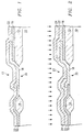
- Referring to Figure 1, an integrated circuit is formed in a
silicon substrate 10.Field oxide regions region 20. Polycrystalline silicon gates (not shown) are generally formed over the active regions to define field effect transistors.Active area 20 insubstrate 10 may be a source/drain region of a field effect transistor. - A
first oxide layer 16 is formed over the integrated circuit, patterned and etched to form afirst opening 17 through the oxide layer exposing a portion of thesubstrate 10. A firstconductive layer 18, generally a doped polysilicon or a polycide, may be formed over the integrated circuit, patterned and etched to form the lower layer of a shared contact region. Asecond oxide layer 22 may then be formed over the integrated circuit.Layer 22 may typically have a thickness of between approximately 900-2000 angstroms. - Referring to Figure 2,
layer 22 is then patterned and etched to form anopening 23 inlayer 22 exposing a portion of the firstconductive layer 18. A secondconductive layer 24 is then formed over thesecond oxide layer 22 and in theopening 23 over the firstconductive layer 18 to form the shared contact.Layer 24 will typically have a thickness of between approximately 500-2000 angstroms.Layer 24 is then lightly doped as shown by the arrows, preferably with a P-type dopant such as boron, to increase the conductivity of the layer or to decrease the layer's resistivity. Device fabrication up to this stage utilizes conventional process steps well known in the art. - Referring to Figure 3, a
third oxide layer 26 is formed over the integrated circuit, patterned and etched to expose aregion 25 of the secondconductive layer 24 not in contact with the underlying firstconductive layer 18.Oxide layer 26 typically has a thickness of between approximately 900-2000 angstroms. -
Region 25 is then implanted with a dopant of opposite conductivity from the dopant implanted across theentire layer 24. If the blanket implant is P-type, a N-type dopant such as arsenic is implanted intoregion 25 as shown by the arrows.Oxide layer 26 acts as a mask over the portion oflayer 24underlying layer 26. Onceregion 25 is implanted with a dopant of the opposite conductivity, aP-N junction 27 is formed betweenregion 25 and the portion oflayer 24 underlyingoxide layer 26. The P-N junction is formed where the two regions of polycrystalline silicon having different conductivity types make contact. TheP-N junction 27 is reverse biased since the N-type region is connected to the power supply. Since the P-N junction is formed in polysilicon, it is leaky, so that some reverse current flows. The P-N junction acts as the resistive load device such as in a CMOS SRAM cell between a N-channel transistor and its power supply. The N-channel transistor is formed elsewhere on the surface of the integrated circuit. - Referring to Figure 4, a
fourth oxide layer 28 is then formed over the integrated circuit.Layer 28 will have a thickness of between approximately 1000-5000 angstroms. - Referring to Figure 5, an etchback step is performed to form a
sidewall oxide spacer 30 on the side ofoxide layer 26 and in the opening ofregion 25. Ametal layer 32 is then deposited to a depth of between approximately 200-1000 angstroms.Metal layer 32 may be any refractory metal, such as titanium, which can be reacted with silicon to form a silicide and increase the layer's conductivity. For purposes of illustration,layer 32 will be referred to as titanium. - Referring to Figure 6,
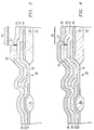
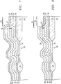
titanium layer 32 is annealed to thermally react with the underlying secondconductive layer 24 inregion 25 not covered by theoxide sidewall spacer 30. Atitanium disilicide layer 36 is formed during the annealing process. Any unreacted titanium remaining after the annealing step is then stripped away. The purpose of forming the silicide layer is to reduce the resistivity of the conductive layer to form the Vcc power supply in thesame polysilicon layer 24 as theresistive load device 27. Theoxide sidewall spacer 30 protects theP-N junction 27 from being silicided during the annealing process. Ifjunction 27 had been silicided, a short circuit condition would have been created across the junction making the resistive load a conductor instead of a high resistance element. - Referring to Figure 7, an alternative method of forming an oxide region to protect the
P-N junction 27 during the siliciding process is shown. Thefifth oxide layer 28 is formed over the integrated circuit as described in connection with Figure 4.Oxide layer 28 is then patterned and etched to form anopening 29 which is smaller thanregion 27. Ametal layer 34, capable of forming a silicide, is formed as above. Again, for purposes of illustration, this layer will be referred to as titanium. The titanium is annealed as described above to react with the underlying secondconductive layer 24 inopening 29. - Referring to Figure 8, any unreacted titanium will be stripped away after forming a
titanium disilicide layer 38. As with thesidewall oxide spacer 30, the portion ofoxide layer 28 remaining after the etch step inregion 25 will protect theP-N junction 27 from being silicided and will prevent a short across the junction. - An advantage of this invention over prior art is that an area of low resistance and an area of high resistance is made in the same polycrystalline silicon layer. The layer can then be used for both the resistive load device and the Vcc power supply or local interconnect. The layer is lightly doped with a dopant of first conductivity type. One region of the layer to become the area for the Vcc power supply is implanted with a dopant of a second and opposite conductivity type. The conductivity types may also be the same conductivity type but of significantly different doping levels. A P-N junction is formed between the two regions in the silicon layer having different conductivities. An oxide layer protects the junction during silicidation of the Vcc power supply area within the silicon layer. No substantial silicidation of the junction occurs and any short of the junction is prevented.
- While the invention has been particularly shown and described with reference to a preferred embodiment, it will be understood by those skilled in the art that various changes in form and detail may be made therein without departing from the spirit and scope of the invention.
- The present invention may provide a method wherein a first conductive layer has a thickness of between approximately 500 to 2000 angstroms, wherein a metal silicide forming layer is deposited to a depth of between approximately 200 to 1000 angstroms, or wherein first and second oxide layers have a thickness of between 900 to 2000 angstroms. The present invention may provide a method, wherein a first conductive layer's first region is implanted with an N-type dopant, and/or a first conductive layer's second region is implanted with a P-type dopant. The present invention may provide a structure in which a first conductivity type is P-type and/or a second conductivity type is N-type.
Claims (16)
- A method of forming a polycrystalline silicon resistive load element in a semiconductor integrated circuit, comprising the steps of:
forming a first conductive layer wherein the first conductive layer has a first region of a first conductivity type and a second region of a second conductivity type wherein a junction is formed between the first and the second regions;
forming a second oxide layer over the second region, the junction and an adjacent portion of the first region of the first conductive layer; and,
forming a silicide region over the first region of the first conductive layer not covered by the second oxide layer. - The method of Claim 1, wherein the first conductive layer's first region is implanted with arsenic.
- The method of Claim 1, wherein the first conductive layer's second region is implanted with boron.
- The method of Claim 1, wherein the forming the second oxide layer step further comprises the steps of:
depositing an undoped oxide layer over the integrated circuit; and,
performing an etchback of the undoped oxide layer to form sidewall oxide spacers on the sidewalls of the second oxide layer covering the junction and a portion of the second region adjacent to the junction. - The method of Claim 1, wherein the forming the second oxide layer step further comprises the steps of:
depositing an undoped oxide layer over the integrated circuit; and,
patterning and etching the undoped oxide layer to form an undoped oxide layer over the second oxide layer, the junction, and a portion of the second region adjacent to the junction. - A method of forming a polycrystalline silicon resistive load element in a semiconductor integrated circuit, comprising the steps of:
forming a lightly doped first conductive layer having a conductivity of a first type;
forming a first oxide layer over the integrated circuit with a first opening therethrough exposing a portion of the first conductive layer;
using the first oxide layer as a mask, implanting the exposed portion of the first conductive layer with a dopant of a second conductivity type to form a junction between the exposed portion and the portion covered by the mask;
forming a second oxide region on a portion of the first oxide layer in the first opening, over the junction and over a portion of the exposed first conductive layer; and,
forming a silicide over the exposed portion of the first conductive layer. - The method of Claim 1 to 6, wherein the first conductive layer is a polysilicon layer.
- The method of Claim 1 to 6, wherein the first conductive layer is a polycide layer.
- The method of Claim 6, wherein the forming a third oxide region step further comprises the steps of:
depositing an undoped oxide layer over the integrated circuit; and,
performing an etchback of the undoped oxide layer to form sidewall oxide spacers on the sidewalls of the second oxide layer. - The method of Claim 6, wherein the forming a fourth oxide region step further comprises the steps of:
depositing an undoped oxide layer over the integrated circuit; and,
patterning and etching the undoped oxide layer to expose a portion of the exposed first conductive layer. - The method of Claim 1 or 6, wherein the silicide forming step further comprises the steps of:
forming a metal silicide forming layer over the integrated circuit;
annealing the metal silicide forming layer; and,
removing any unreacted metal from the metal silicide forming layer. - A structure consisting of a portion of a semiconductor integrated circuit, comprising:
a first conductive layer having a first region of a first conductivity type and a second region of a second conductivity type and having a junction between the first and second regions;
a first oxide region disposed over the first region, the junction and a portion of the second region adjacent to the junction; and
a silicide region disposed over the portion of the second region not covered by the first oxide region. - The method of Claim 1 or 6, or the structure of Claim 12, wherein the first oxide region or layer is disposed over a second conductive layer and wherein the first oxide region or layer has an opening therethrough exposing a portion of the second conductive layer.
- The method of Claim 1 or 6, or the structure of Claim 12, wherein the first conductive layer is further disposed over the exposed portion of the second conductive layer.
- The method of Claim 11 or the structure of Claim 12, wherein the silicide is a refractory metal silicide.
- The method of Claim 15, wherein the refractory metal is titanium.
Applications Claiming Priority (2)
| Application Number | Priority Date | Filing Date | Title |
|---|---|---|---|
| US07/769,171 US5182627A (en) | 1991-09-30 | 1991-09-30 | Interconnect and resistor for integrated circuits |
| US769171 | 1991-09-30 |
Publications (2)
| Publication Number | Publication Date |
|---|---|
| EP0536902A1 true EP0536902A1 (en) | 1993-04-14 |
| EP0536902B1 EP0536902B1 (en) | 1999-03-31 |
Family
ID=25084678
Family Applications (1)
| Application Number | Title | Priority Date | Filing Date |
|---|---|---|---|
| EP92308273A Expired - Lifetime EP0536902B1 (en) | 1991-09-30 | 1992-09-11 | Interconnect and resistor for integrated circuits |
Country Status (4)
| Country | Link |
|---|---|
| US (2) | US5182627A (en) |
| EP (1) | EP0536902B1 (en) |
| JP (1) | JPH05259401A (en) |
| DE (1) | DE69228786T2 (en) |
Families Citing this family (17)
| Publication number | Priority date | Publication date | Assignee | Title |
|---|---|---|---|---|
| US5273924A (en) * | 1991-08-30 | 1993-12-28 | Micron Technology, Inc. | Method for forming an SRAM by minimizing diffusion of conductivity enhancing impurities from one region of a polysilicon layer to another region |
| JP2748070B2 (en) * | 1992-05-20 | 1998-05-06 | 三菱電機株式会社 | Semiconductor device and manufacturing method thereof |
| KR960001176B1 (en) * | 1992-12-02 | 1996-01-19 | 현대전자산업주식회사 | Semiconductor connection apparatus and the manufacturing |
| US5478771A (en) * | 1993-05-28 | 1995-12-26 | Sgs-Thomson Microelectronics, Inc. | Method of forming local interconnect structure without P-N junction between active elements |
| JP2934738B2 (en) | 1994-03-18 | 1999-08-16 | セイコーインスツルメンツ株式会社 | Semiconductor device and manufacturing method thereof |
| KR950034754A (en) * | 1994-05-06 | 1995-12-28 | 윌리엄 이. 힐러 | Method for forming polysilicon resistance and resistance made from this method |
| US5464794A (en) * | 1994-05-11 | 1995-11-07 | United Microelectronics Corporation | Method of forming contact openings having concavo-concave shape |
| US5578873A (en) * | 1994-10-12 | 1996-11-26 | Micron Technology, Inc. | Integrated circuitry having a thin film polysilicon layer in ohmic contact with a conductive layer |
| US5489797A (en) * | 1994-12-19 | 1996-02-06 | Sgs-Thomson Microelectronics, Inc. | Local interconnect structure |
| EP0746027A3 (en) * | 1995-05-03 | 1998-04-01 | Applied Materials, Inc. | Polysilicon/tungsten silicide multilayer composite formed on an integrated circuit structure, and improved method of making same |
| US5909617A (en) | 1995-11-07 | 1999-06-01 | Micron Technology, Inc. | Method of manufacturing self-aligned resistor and local interconnect |
| US5994182A (en) | 1996-01-18 | 1999-11-30 | Micron Technology, Inc. | Method of reducing outdiffusion from a doped three-dimensional polysilicon film into substrate by using angled implants |
| US5763313A (en) * | 1996-03-13 | 1998-06-09 | United Microelectronics Corp. | Process for fabricating shield for polysilicon load |
| US5883417A (en) * | 1996-06-27 | 1999-03-16 | Winbond Electronics Corporation | Poly-load resistor for SRAM cell |
| TW330334B (en) * | 1997-08-23 | 1998-04-21 | Winbond Electronics Corp | Static random access memory polysilicon load structure and manufacturing method |
| JP4392867B2 (en) | 1998-02-06 | 2010-01-06 | 株式会社ルネサステクノロジ | Semiconductor device and manufacturing method thereof |
| US6054359A (en) * | 1999-06-14 | 2000-04-25 | Taiwan Semiconductor Manufacturing Company | Method for making high-sheet-resistance polysilicon resistors for integrated circuits |
Citations (5)
| Publication number | Priority date | Publication date | Assignee | Title |
|---|---|---|---|---|
| US4251876A (en) * | 1978-11-03 | 1981-02-17 | Mostek Corporation | Extremely low current load device for integrated circuit |
| EP0112097A2 (en) * | 1982-12-15 | 1984-06-27 | THORN EMI North America Inc. | Polysilicon resistor with low thermal activation energy |
| EP0113405A2 (en) * | 1982-12-13 | 1984-07-18 | International Business Machines Corporation | Method for making semiconductor resistors |
| EP0166964A1 (en) * | 1984-06-04 | 1986-01-08 | International Business Machines Corporation | A double level polysilicon semiconductor structure |
| EP0310351A1 (en) * | 1987-09-30 | 1989-04-05 | Texas Instruments Incorporated | Static memory using Schottky technology |
Family Cites Families (8)
| Publication number | Priority date | Publication date | Assignee | Title |
|---|---|---|---|---|
| NL190710C (en) * | 1978-02-10 | 1994-07-01 | Nec Corp | Integrated semiconductor chain. |
| FR2534415A1 (en) * | 1982-10-07 | 1984-04-13 | Cii Honeywell Bull | METHOD FOR MANUFACTURING ELECTRICAL RESISTORS IN POLYCRYSTALLINE SEMICONDUCTOR MATERIAL AND RESULTING INTEGRATED CIRCUIT ARRANGEMENT |
| IT1186485B (en) * | 1985-12-20 | 1987-11-26 | Sgs Microelettronica Spa | MONOLITHIC INTEGRATED CIRCUIT, IN PARTICULAR OF THE MOS OR CMOS TYPE AND PROCESS FOR THE REALIZATION OF SUCH CIRCUIT |
| US4975575A (en) * | 1987-03-31 | 1990-12-04 | Brandeis University | Method of and apparatus for detecting radon |
| JPH01143252A (en) * | 1987-11-27 | 1989-06-05 | Nec Corp | Semiconductor device |
| JP2829992B2 (en) * | 1988-11-10 | 1998-12-02 | セイコーエプソン株式会社 | Semiconductor device |
| US4948747A (en) * | 1989-12-18 | 1990-08-14 | Motorola, Inc. | Method of making an integrated circuit resistor |
| US5068201A (en) * | 1990-05-31 | 1991-11-26 | Sgs-Thomson Microelectronics, Inc. | Method for forming a high valued resistive load element and low resistance interconnect for integrated circuits |
-
1991
- 1991-09-30 US US07/769,171 patent/US5182627A/en not_active Expired - Lifetime
-
1992
- 1992-07-09 US US07/911,167 patent/US5348901A/en not_active Expired - Lifetime
- 1992-09-11 DE DE69228786T patent/DE69228786T2/en not_active Expired - Fee Related
- 1992-09-11 EP EP92308273A patent/EP0536902B1/en not_active Expired - Lifetime
- 1992-09-30 JP JP4261901A patent/JPH05259401A/en active Pending
Patent Citations (5)
| Publication number | Priority date | Publication date | Assignee | Title |
|---|---|---|---|---|
| US4251876A (en) * | 1978-11-03 | 1981-02-17 | Mostek Corporation | Extremely low current load device for integrated circuit |
| EP0113405A2 (en) * | 1982-12-13 | 1984-07-18 | International Business Machines Corporation | Method for making semiconductor resistors |
| EP0112097A2 (en) * | 1982-12-15 | 1984-06-27 | THORN EMI North America Inc. | Polysilicon resistor with low thermal activation energy |
| EP0166964A1 (en) * | 1984-06-04 | 1986-01-08 | International Business Machines Corporation | A double level polysilicon semiconductor structure |
| EP0310351A1 (en) * | 1987-09-30 | 1989-04-05 | Texas Instruments Incorporated | Static memory using Schottky technology |
Non-Patent Citations (3)
| Title |
|---|
| IEEE JOURNAL OF SOLID-STATE CIRCUITS vol. SC-20, no. 5, October 1985, NEW YORK US pages 924 - 928 S. YAMAMOTO ET AL * |
| PATENT ABSTRACTS OF JAPAN vol. 007, no. 162 (E-187)15 July 1983 & JP-A-58 070 568 ( NIPPON DENKI K K ) 27 April 1983 * |
| PATENT ABSTRACTS OF JAPAN vol. 11, no. 171 (E-512)2 June 1987 & JP-A-62 007 151 ( HITACHI ) 14 January 1987 * |
Also Published As
| Publication number | Publication date |
|---|---|
| DE69228786D1 (en) | 1999-05-06 |
| JPH05259401A (en) | 1993-10-08 |
| US5182627A (en) | 1993-01-26 |
| US5348901A (en) | 1994-09-20 |
| DE69228786T2 (en) | 1999-11-11 |
| EP0536902B1 (en) | 1999-03-31 |
Similar Documents
| Publication | Publication Date | Title |
|---|---|---|
| EP0536902B1 (en) | Interconnect and resistor for integrated circuits | |
| US5334862A (en) | Thin film transistor (TFT) loads formed in recessed plugs | |
| EP0523830B1 (en) | A stacked CMOS SRAM cell with polysilicon transistor load | |
| US5177030A (en) | Method of making self-aligned vertical intrinsic resistance | |
| US5907176A (en) | Integrated circuits and SRAM memory cells | |
| EP0517368B1 (en) | Local interconnect for integrated circuits | |
| EP0460833A1 (en) | Field effect device with polycrystaline silicon channel | |
| EP1075016B1 (en) | Self-aligned precise high sheet RHO resistor for mixed-signal application | |
| US6054353A (en) | Short turn around time mask ROM process | |
| EP0459618B1 (en) | Polycrystalline silicon resistors for integrated circuits | |
| US5462894A (en) | Method for fabricating a polycrystalline silicon resistive load element in an integrated circuit | |
| US6717233B1 (en) | Method for fabricating resistors within semiconductor integrated circuit devices | |
| US5883417A (en) | Poly-load resistor for SRAM cell | |
| US5241206A (en) | Self-aligned vertical intrinsic resistance | |
| US4785342A (en) | Static random access memory having structure of first-, second- and third-level conductive films | |
| US5068201A (en) | Method for forming a high valued resistive load element and low resistance interconnect for integrated circuits | |
| US6362039B1 (en) | Self-aligned resistor and local interconnect | |
| JP3064472B2 (en) | Contact structure of integrated circuit device | |
| US5686338A (en) | Process for fabricating high-resistance load resistors using dummy polysilicon in four-transistor SRAM devices | |
| US5926698A (en) | Semiconductor memory device and method of fabricating the same | |
| US5268325A (en) | Method for fabricating a polycrystalline silicon resistive load element in an integrated circuit | |
| US6165831A (en) | Method of fabricating a buried contact in a static random access memory | |
| EP0517408B1 (en) | Sram cell and structure with polycrystalline p-channel load devices | |
| KR100265337B1 (en) | Manufacturing method for a high load resistor type of sram cell | |
| EP0767491A2 (en) | Method of forming a contact |
Legal Events
| Date | Code | Title | Description |
|---|---|---|---|
| PUAI | Public reference made under article 153(3) epc to a published international application that has entered the european phase |
Free format text: ORIGINAL CODE: 0009012 |
|
| AK | Designated contracting states |
Kind code of ref document: A1 Designated state(s): DE FR GB IT |
|
| 17P | Request for examination filed |
Effective date: 19931005 |
|
| 17Q | First examination report despatched |
Effective date: 19951010 |
|
| GRAG | Despatch of communication of intention to grant |
Free format text: ORIGINAL CODE: EPIDOS AGRA |
|
| GRAG | Despatch of communication of intention to grant |
Free format text: ORIGINAL CODE: EPIDOS AGRA |
|
| GRAH | Despatch of communication of intention to grant a patent |
Free format text: ORIGINAL CODE: EPIDOS IGRA |
|
| GRAH | Despatch of communication of intention to grant a patent |
Free format text: ORIGINAL CODE: EPIDOS IGRA |
|
| GRAA | (expected) grant |
Free format text: ORIGINAL CODE: 0009210 |
|
| RAP3 | Party data changed (applicant data changed or rights of an application transferred) |
Owner name: STMICROELECTRONICS, INC. |
|
| AK | Designated contracting states |
Kind code of ref document: B1 Designated state(s): DE FR GB IT |
|
| REF | Corresponds to: |
Ref document number: 69228786 Country of ref document: DE Date of ref document: 19990506 |
|
| ET | Fr: translation filed | ||
| PLBE | No opposition filed within time limit |
Free format text: ORIGINAL CODE: 0009261 |
|
| STAA | Information on the status of an ep patent application or granted ep patent |
Free format text: STATUS: NO OPPOSITION FILED WITHIN TIME LIMIT |
|
| 26N | No opposition filed | ||
| PG25 | Lapsed in a contracting state [announced via postgrant information from national office to epo] |
Ref country code: DE Free format text: LAPSE BECAUSE OF NON-PAYMENT OF DUE FEES Effective date: 20000701 |
|
| PGFP | Annual fee paid to national office [announced via postgrant information from national office to epo] |
Ref country code: FR Payment date: 20010911 Year of fee payment: 10 |
|
| PGFP | Annual fee paid to national office [announced via postgrant information from national office to epo] |
Ref country code: GB Payment date: 20010912 Year of fee payment: 10 |
|
| REG | Reference to a national code |
Ref country code: GB Ref legal event code: IF02 |
|
| PG25 | Lapsed in a contracting state [announced via postgrant information from national office to epo] |
Ref country code: GB Free format text: LAPSE BECAUSE OF NON-PAYMENT OF DUE FEES Effective date: 20020911 |
|
| GBPC | Gb: european patent ceased through non-payment of renewal fee |
Effective date: 20020911 |
|
| PG25 | Lapsed in a contracting state [announced via postgrant information from national office to epo] |
Ref country code: FR Free format text: LAPSE BECAUSE OF NON-PAYMENT OF DUE FEES Effective date: 20030603 |
|
| REG | Reference to a national code |
Ref country code: FR Ref legal event code: ST |
|
| PG25 | Lapsed in a contracting state [announced via postgrant information from national office to epo] |
Ref country code: IT Free format text: LAPSE BECAUSE OF NON-PAYMENT OF DUE FEES;WARNING: LAPSES OF ITALIAN PATENTS WITH EFFECTIVE DATE BEFORE 2007 MAY HAVE OCCURRED AT ANY TIME BEFORE 2007. THE CORRECT EFFECTIVE DATE MAY BE DIFFERENT FROM THE ONE RECORDED. Effective date: 20050911 |