EP0536756B1 - A microcomputer and its option setting circuit - Google Patents
A microcomputer and its option setting circuit Download PDFInfo
- Publication number
- EP0536756B1 EP0536756B1 EP92117219A EP92117219A EP0536756B1 EP 0536756 B1 EP0536756 B1 EP 0536756B1 EP 92117219 A EP92117219 A EP 92117219A EP 92117219 A EP92117219 A EP 92117219A EP 0536756 B1 EP0536756 B1 EP 0536756B1
- Authority
- EP
- European Patent Office
- Prior art keywords
- memory
- microcomputer
- option
- circuit
- option setting
- Prior art date
- Legal status (The legal status is an assumption and is not a legal conclusion. Google has not performed a legal analysis and makes no representation as to the accuracy of the status listed.)
- Expired - Lifetime
Links
Images



Classifications
-
- G—PHYSICS
- G06—COMPUTING OR CALCULATING; COUNTING
- G06F—ELECTRIC DIGITAL DATA PROCESSING
- G06F1/00—Details not covered by groups G06F3/00 - G06F13/00 and G06F21/00
- G06F1/24—Resetting means
-
- G—PHYSICS
- G06—COMPUTING OR CALCULATING; COUNTING
- G06F—ELECTRIC DIGITAL DATA PROCESSING
- G06F12/00—Accessing, addressing or allocating within memory systems or architectures
- G06F12/02—Addressing or allocation; Relocation
- G06F12/06—Addressing a physical block of locations, e.g. base addressing, module addressing, memory dedication
- G06F12/0638—Combination of memories, e.g. ROM and RAM such as to permit replacement or supplementing of words in one module by words in another module
Definitions
- the present invention relates to a microcomputer, and more particularly, to an option setting circuit for setting an option of a function of the microcomputer.
- One-chip microcomputers are provided with option setting circuits. This is because there are occasions where options are changed in accordance with the arrangements of peripheral integrated circuits (ICs) and discrete parts.
- Option setting circuits are also used for changing options when specifications are changed in developing a system for an IC chip for evaluating an application program for one-chip microcomputers.
- Figs. 1 and 2 show an example of a conventional option setting circuit with respect to an I/O (input/output) circuit.
- An I/O circuit is provided with an invertor 51 and a p-channel MOS (metal oxide semiconductor) transistor 1 for pulling up an input line L of the invertor 51 to a power supply line 2.
- MOS metal oxide semiconductor
- an input terminal of the inverter 51 is connected to an external switching circuit through an input pad 50, if the switching circuit is a CMOS (complementary metal oxide semiconductor), it is unnecessary to pull up the input terminal of the invertor 51 to the power supply line 2. This is because signals having a value of 0 and signals having a value of 1 are produced by the switching circuit and inputted into the I/O circuit. Therefore, the transistor 1 is set to OFF state.
- CMOS complementary metal oxide semiconductor
- the switching circuit consists only of an n-channel MOS transistor, since only "0" signals are inputted to the input pad 50, it is required to produce "1" signals at the I/O circuit. Therefore, in that case, it is necessary that the transistor 1 be always ON.
- the transistor 1 When the transistor 1 is ON, if the external switching circuit is OFF, an input of the invertor 51 is 1 (a VDD voltage of the power supply line 2), and if the external switching circuit is ON, the input of the invertor 51 is 0 since "0" signals are inputted.
- Fig. 1 shows a method in which whether to connect a switch 4 connected to an input of the transistor 1 to the power supply line 2 or to a ground line 3 is determined in the masking process at the time of manufacture of the microcomputer
- Fig. 2 shows a method in which ON/OFF of the transistor 1 is set by determining whether to set an output of a D-type flip-flop 5 connected to a control electrode of the transistor 1 to 1 or to 0.
- an option memory 6 is provided, and the output of the flip-flop 5 is decided based on an output data (1 or 0) of the memory 6.
- the condition of the transistor 1 is set based on the output.
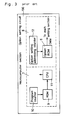
- a microcomputer having the above-mentioned option memory 6 is formed as one chip 100 including a microcomputer section 7 and an option setting circuit 8.
- the microcomputer section 7 includes a memory (ROM [read only memory]) 9 for operation of a microcomputer, a program counter 10 which drives the memory 9, and a CPU (central processing unit) 11 which receives an output data of the memory 9.
- the option setting circuit 8 includes the-option memory 6 and an option setting address counter 12 which drives the memory 6.
- Fig. 4 shows the arrangement of the conventional option setting circuit in further detail.
- a timing generator 13, an address decoder 14, an instruction decoder 15 and an address decoder 16 are provided in addition to the memories 6 and 9, the program counter 10 and the address counter 12.
- the conventional option setting circuit is provided with the addressing counter 12 and the address decoder 16 which are exclusively used for setting an output data of the option memory as described above, a larger chip is required. It is generally difficult to realize a low-cost, highly-reliable semiconductor apparatus if the circuit is large in size.
- EP-A-0 287 337 discloses programmable logic device circuit (PLD) comprising:
- the setting of options is performed by a logic circuit, without using a memory for options. Therefore, it is not necessary, either, to perform addressing of the memory. In other words, it is not necessary to a method memory addressing circuit between the purposes of running a computer program and setting options.
- An object of the present invention is to provide a microcomputer having an option setting function which microcomputer is not large in circuit size and an option setting circuit for the microcomputer.
- Fig. 5 shows a circuit embodying the present invention. The following are provided on one chip: a timing generator 21; a program counter 22 which operates in response to a timing signal generated by the timing generator 21; an address decoder 23 which decodes an output of the program counter 22 and provides a decoded output to a memory (ROM) 25 of the microcomputer and to an option memory 27; and a reset control signal producing circuit 28 which produces a reset control signal based on a reset signal provided from an external reset signal producing circuit and controls operation periods of the memories 25 and 27.
- Numeral 26 represents an instruction decoder.
- An output of the memory 27 is provided to a flip-flop 5 which controls a transistor 1 of an I/O circuit as shown in Fig. 7.
- the reset control signal producing circuit 28 deactivates the memory 25 by providing a high-level voltage thereto for a predetermined period of time after a reset state set by the external reset signal is released, and activates the memory 25 thereafter. Consequently, after the reset state set by the external reset signal is released, the microcomputer is provided with a reset period T1 and an operation period T2 as shown in (a) of Fig. 6. During the reset period T1, an operation period W is provided to the memory 27 by a control signal (d) produced by the reset control signal producing circuit 28. The memory 27 outputs an option setting data based on an output of the address decoder 23 (consequently, an output of the program counter 22) during the period W to thereby set an option of the microcomputer.
- While the activation and deactivation of the memories 25 and 27 are controlled by an output of the reset control signal producing circuit 28, they may be controlled by connecting a switching circuit such as a multiplexer to an output side of the address decoder and then alternatively providing to the memories 25 and 27 an output of the address decoder 23 (consequently, an output of the program counter 22) by controlling the switching circuit based on an output of the reset controlling signal producing circuit 28.
- a switching circuit such as a multiplexer
- Fig. 7 shows a case where the option setting is made in an I/O circuit as shown in Fig. 2.
- a memory 6 and a latch circuit 5 are simultaneously opened when the level of a specified address data is changed to low by an address data bus line 30 based on an address data as shown at P.
- an option data is inputted from the option memory 6 to the latch circuit 5 through a data bus line 31.
- Content of the option setting is not limited to the above example.
- a function operation or an output content may be changed as an option.
- the microcomputer of the above-described embodiment may be a one-time microcomputer where a memory is molded in resin and can be written only once. Moreover, it may be a multi-time microcomputer where a memory is not molded in resin and can be rewritten any number of times.
Landscapes
- Engineering & Computer Science (AREA)
- Theoretical Computer Science (AREA)
- Physics & Mathematics (AREA)
- General Engineering & Computer Science (AREA)
- General Physics & Mathematics (AREA)
- Microcomputers (AREA)
Description
Claims (5)
- An option setting circuit for use in a microcomputer comprising:a first memory (25) for operation of the microcomputer;a second memory (27) for storing option data relating to a function of the microcomputer;a program counter (22) ;an address decoder (23) receiving the output of said program counter;means for directing an output of the address decoder to said first memory and said second memory;memory controlling means (28) for deactivating the first memory for a predetermined period of time after an external reset signal has been received by the microcomputer and activating the second memory while the first memory is being deactivated in order to retrieve said stored option data.
- An option setting circuit according to claim 1, wherein the memory controlling means (28) provides an output of the program counter to the second memory during a reset period of the microcomputer.
- An option setting circuit according to any of the preceding claims, further comprising:an I/O circuit having a switch transistor (1) connected between a signal line and a power supply line (2);a latch circuit (5) which latches a data from said second memory and provides a latch output to a control electrode of the switch transistor (1).
- An option setting circuit according to claim 3, wherein the latch circuit (5) is a D-type flip-flop.
- A microcomputer comprising an option setting circuit according to any of the preceding claims.
Applications Claiming Priority (2)
| Application Number | Priority Date | Filing Date | Title |
|---|---|---|---|
| JP290965/91 | 1991-10-09 | ||
| JP3290965A JPH05101200A (en) | 1991-10-09 | 1991-10-09 | Option setting circuit |
Publications (2)
| Publication Number | Publication Date |
|---|---|
| EP0536756A1 EP0536756A1 (en) | 1993-04-14 |
| EP0536756B1 true EP0536756B1 (en) | 1998-05-27 |
Family
ID=17762738
Family Applications (1)
| Application Number | Title | Priority Date | Filing Date |
|---|---|---|---|
| EP92117219A Expired - Lifetime EP0536756B1 (en) | 1991-10-09 | 1992-10-08 | A microcomputer and its option setting circuit |
Country Status (3)
| Country | Link |
|---|---|
| EP (1) | EP0536756B1 (en) |
| JP (1) | JPH05101200A (en) |
| DE (1) | DE69225665T2 (en) |
Families Citing this family (2)
| Publication number | Priority date | Publication date | Assignee | Title |
|---|---|---|---|---|
| FR2700402B1 (en) * | 1993-01-13 | 1995-04-07 | Sgs Thomson Microelectronics | Microcontroller with electrically programmable multimode memory. |
| FR2790117B1 (en) * | 1999-02-19 | 2001-09-14 | St Microelectronics Sa | METHOD FOR CONFIGURING A MICROCONTROLLER IN INITIALIZATION MODE |
Citations (1)
| Publication number | Priority date | Publication date | Assignee | Title |
|---|---|---|---|---|
| EP0287337A2 (en) * | 1987-04-14 | 1988-10-19 | Rohm Corporation | Programming circuit for programmable logic array I/O cell |
-
1991
- 1991-10-09 JP JP3290965A patent/JPH05101200A/en active Pending
-
1992
- 1992-10-08 DE DE1992625665 patent/DE69225665T2/en not_active Expired - Fee Related
- 1992-10-08 EP EP92117219A patent/EP0536756B1/en not_active Expired - Lifetime
Patent Citations (1)
| Publication number | Priority date | Publication date | Assignee | Title |
|---|---|---|---|---|
| EP0287337A2 (en) * | 1987-04-14 | 1988-10-19 | Rohm Corporation | Programming circuit for programmable logic array I/O cell |
Also Published As
| Publication number | Publication date |
|---|---|
| DE69225665D1 (en) | 1998-07-02 |
| DE69225665T2 (en) | 1999-01-28 |
| EP0536756A1 (en) | 1993-04-14 |
| JPH05101200A (en) | 1993-04-23 |
Similar Documents
| Publication | Publication Date | Title |
|---|---|---|
| US4590553A (en) | Microcomputer with power-save output instructions | |
| US4752930A (en) | Watch dog timer | |
| KR920004288B1 (en) | Data processors and methods for selectively disabling power-down commands | |
| JPH0157378B2 (en) | ||
| US6557107B1 (en) | Power-saving mode release error detection and recovery logic circuit for microcontroller devices | |
| US5767694A (en) | Information processing apparatus with a mode setting circuit | |
| KR100210557B1 (en) | Input circuit for mode setting | |
| EP0532790A1 (en) | One-chip microcomputer | |
| US5770959A (en) | Circuit for providing the power-up state of an electrical device | |
| US7467294B2 (en) | Microcomputer with mode decoder operable upon receipt of either power-on or external reset signal | |
| US5808490A (en) | Method and circuit for controlling a bus in system and semiconductor integrated circuit device using the same, wherein the controlling circuit comprises a latch for holding a voltage level on the bus | |
| EP0536756A1 (en) | A microcomputer and its option setting circuit | |
| US6631467B1 (en) | Microcomputer timing control circuit provided with internal reset signal generator triggered by external reset signal | |
| US6625731B1 (en) | Method of configuring a microcontroller during reset mode by generating auxiliary oscillator signal as supply voltage ramps up to read option word from central memory | |
| US5495196A (en) | User controlled reset circuit with fast recovery | |
| US5559981A (en) | Pseudo static mask option register and method therefor | |
| US5727166A (en) | Buffer with drive characteristics controllable by software | |
| US5594362A (en) | Gatable level-pulling circuit | |
| US5438279A (en) | Option setting circuit for interface circuit | |
| EP0419117B1 (en) | Wafer-scale semiconductor device having fail-safe circuit | |
| KR100228562B1 (en) | Remote controller | |
| JP2644111B2 (en) | Input/Output Circuit | |
| JPH1141086A (en) | Integrated circuit | |
| KR100407569B1 (en) | Oscillator circuit with oscillation control function | |
| JPH05291932A (en) | Electronic circuit |
Legal Events
| Date | Code | Title | Description |
|---|---|---|---|
| PUAI | Public reference made under article 153(3) epc to a published international application that has entered the european phase |
Free format text: ORIGINAL CODE: 0009012 |
|
| AK | Designated contracting states |
Kind code of ref document: A1 Designated state(s): DE FR GB IT NL |
|
| 17P | Request for examination filed |
Effective date: 19931008 |
|
| 17Q | First examination report despatched |
Effective date: 19960705 |
|
| GRAG | Despatch of communication of intention to grant |
Free format text: ORIGINAL CODE: EPIDOS AGRA |
|
| GRAG | Despatch of communication of intention to grant |
Free format text: ORIGINAL CODE: EPIDOS AGRA |
|
| GRAH | Despatch of communication of intention to grant a patent |
Free format text: ORIGINAL CODE: EPIDOS IGRA |
|
| GRAH | Despatch of communication of intention to grant a patent |
Free format text: ORIGINAL CODE: EPIDOS IGRA |
|
| GRAA | (expected) grant |
Free format text: ORIGINAL CODE: 0009210 |
|
| AK | Designated contracting states |
Kind code of ref document: B1 Designated state(s): DE FR GB IT NL |
|
| PG25 | Lapsed in a contracting state [announced via postgrant information from national office to epo] |
Ref country code: FR Free format text: LAPSE BECAUSE OF FAILURE TO SUBMIT A TRANSLATION OF THE DESCRIPTION OR TO PAY THE FEE WITHIN THE PRESCRIBED TIME-LIMIT Effective date: 19980527 |
|
| REF | Corresponds to: |
Ref document number: 69225665 Country of ref document: DE Date of ref document: 19980702 |
|
| ITF | It: translation for a ep patent filed | ||
| EN | Fr: translation not filed | ||
| PLBE | No opposition filed within time limit |
Free format text: ORIGINAL CODE: 0009261 |
|
| 26N | No opposition filed | ||
| PGFP | Annual fee paid to national office [announced via postgrant information from national office to epo] |
Ref country code: NL Payment date: 19991027 Year of fee payment: 8 |
|
| PG25 | Lapsed in a contracting state [announced via postgrant information from national office to epo] |
Ref country code: NL Free format text: LAPSE BECAUSE OF NON-PAYMENT OF DUE FEES Effective date: 20010501 |
|
| NLV4 | Nl: lapsed or anulled due to non-payment of the annual fee |
Effective date: 20010501 |
|
| PGFP | Annual fee paid to national office [announced via postgrant information from national office to epo] |
Ref country code: GB Payment date: 20010912 Year of fee payment: 10 |
|
| PGFP | Annual fee paid to national office [announced via postgrant information from national office to epo] |
Ref country code: DE Payment date: 20011220 Year of fee payment: 10 |
|
| REG | Reference to a national code |
Ref country code: GB Ref legal event code: IF02 |
|
| PG25 | Lapsed in a contracting state [announced via postgrant information from national office to epo] |
Ref country code: GB Free format text: LAPSE BECAUSE OF NON-PAYMENT OF DUE FEES Effective date: 20021008 |
|
| PG25 | Lapsed in a contracting state [announced via postgrant information from national office to epo] |
Ref country code: DE Free format text: LAPSE BECAUSE OF NON-PAYMENT OF DUE FEES Effective date: 20030501 |
|
| GBPC | Gb: european patent ceased through non-payment of renewal fee |
Effective date: 20021008 |
|
| PG25 | Lapsed in a contracting state [announced via postgrant information from national office to epo] |
Ref country code: IT Free format text: LAPSE BECAUSE OF NON-PAYMENT OF DUE FEES;WARNING: LAPSES OF ITALIAN PATENTS WITH EFFECTIVE DATE BEFORE 2007 MAY HAVE OCCURRED AT ANY TIME BEFORE 2007. THE CORRECT EFFECTIVE DATE MAY BE DIFFERENT FROM THE ONE RECORDED. Effective date: 20051008 |