EP0536737B1 - Information recording/reproducing apparatus for optical information recording medium - Google Patents
Information recording/reproducing apparatus for optical information recording medium Download PDFInfo
- Publication number
- EP0536737B1 EP0536737B1 EP92117178A EP92117178A EP0536737B1 EP 0536737 B1 EP0536737 B1 EP 0536737B1 EP 92117178 A EP92117178 A EP 92117178A EP 92117178 A EP92117178 A EP 92117178A EP 0536737 B1 EP0536737 B1 EP 0536737B1
- Authority
- EP
- European Patent Office
- Prior art keywords
- motion
- optical head
- information recording
- output
- detecting
- Prior art date
- Legal status (The legal status is an assumption and is not a legal conclusion. Google has not performed a legal analysis and makes no representation as to the accuracy of the status listed.)
- Expired - Lifetime
Links
Images


Classifications
-
- G—PHYSICS
- G11—INFORMATION STORAGE
- G11B—INFORMATION STORAGE BASED ON RELATIVE MOVEMENT BETWEEN RECORD CARRIER AND TRANSDUCER
- G11B7/00—Recording or reproducing by optical means, e.g. recording using a thermal beam of optical radiation by modifying optical properties or the physical structure, reproducing using an optical beam at lower power by sensing optical properties; Record carriers therefor
- G11B7/08—Disposition or mounting of heads or light sources relatively to record carriers
- G11B7/085—Disposition or mounting of heads or light sources relatively to record carriers with provision for moving the light beam into, or out of, its operative position or across tracks, otherwise than during the transducing operation, e.g. for adjustment or preliminary positioning or track change or selection
- G11B7/08505—Methods for track change, selection or preliminary positioning by moving the head
- G11B7/08529—Methods and circuits to control the velocity of the head as it traverses the tracks
-
- G—PHYSICS
- G11—INFORMATION STORAGE
- G11B—INFORMATION STORAGE BASED ON RELATIVE MOVEMENT BETWEEN RECORD CARRIER AND TRANSDUCER
- G11B7/00—Recording or reproducing by optical means, e.g. recording using a thermal beam of optical radiation by modifying optical properties or the physical structure, reproducing using an optical beam at lower power by sensing optical properties; Record carriers therefor
- G11B7/08—Disposition or mounting of heads or light sources relatively to record carriers
- G11B7/085—Disposition or mounting of heads or light sources relatively to record carriers with provision for moving the light beam into, or out of, its operative position or across tracks, otherwise than during the transducing operation, e.g. for adjustment or preliminary positioning or track change or selection
- G11B7/08505—Methods for track change, selection or preliminary positioning by moving the head
- G11B7/08541—Methods for track change, selection or preliminary positioning by moving the head involving track counting to determine position
Definitions
- the present invention relates to an information recording and reproducing apparatus for an optical information recording and reproducing apparatus for an optical information recording medium wherein information is recorded by forming a pit upon application of a light beam to the recording medium while aligning an optical head to a track position, and information is read from a pit by using the light beam.
- a means for generating a tracking error signal whose polarity changes between a positive polarity and negative polarity in response to a track traverse by the optical head.
- a track traverse detecting signal is generated by comparing the tracking error signal with a reference signal.
- the apparatus uses a fixed reference signal so that a tracking error signal of a low level is not detected in some case. Furthermore, when noises having substantially a large level are generated in the circuit, these noises may be detected as a track traverse, thereby forming an incorrect track traverse detecting signal. Further, if the optical system is adjusted improperly, a shoulder is generated on a tracking error signal, thereby forming an incorrect track traverse detecting signal. Still further, an incorrect track traverse detecting signal may be generated by a distortion of the tracking error signal caused by dusts or scratches on the surface of an optical image recording medium.
- EP-A-0. 090 379 discloses a data track searching device capable of switching between two modes; one being the rough searching mode in which a transducer is displaced at a high velocity to a desired track and the other being the fine searching mode which follows the rough searching mode and in which the transducer is displaced at a relative low velocity and positioned over the proper or desired track.
- the operating point of a tracking element is shifted or deviated as a result of the high-velocity displacement of the transducer in the rough searching mode so that stable searching cannot be ensured.
- the acceleration of the transducer in the rough searching mode is detected and a signal representative of the thus detected acceleration is applied to the tracking element so that the shift or deviation of the operating point of the tracking element can substantially made nil.
- EP-A-0 441 969 discloses a seek circuit for moving an optical pickup to a target track set on an optical disk.
- the seek circuit determines the address of the current track from the address information in reproduced signals from the optical disk, generates a reference value which changes with time during the period the pickup moves to the address of the target track from the address of the current track, and drives means for causing movement of the optical pickup in the radial direction of the optical disk in accordance with the difference between the address of the current track and the reference value. In this manner, a high-speed seek operation is achieved without using a speed sensor.
- the present invention provides an information recording and reproducing apparatus for an optical information recording medium for recording and reproducing information to and from the optical information recording medium by scanning each track of the medium with a light beam from an optical head, the optical beam being moved from a first position to a second position on the medium through a combination of a far jump driving the optical head and a near jump driving an objective lens assembled with the optical head, comprising:
- the position reading means scans an optical information recording medium to obtain present address information.
- This address information is stored in the position storage means, and supplied via the switching means to the motion direction designating means and motion distance calculating means.
- the address information is compared with the target position from the target position receiving means to obtain a motion direction and motion distance.
- the motion amount detecting means detects the motion amount of the optical head in accordance with a signal generated by the traverse signal generating means. This motion amount is supplied via the switching means to the motion direction designating means and motion distance calculating means.
- the switching means selects an output of the position storage means when an output of the motion amount detecting means is zero, and an output of the motion amount detecting means when the output is not zero.
- the selected output is supplied to the motion direction designating means and motion distance calculating means.
- An output of the motion direction designating means is supplied to the driving means.
- An output of the motion distance calculating means is supplied to the motion speed controlling means whose output is supplied to the driving means. If the motion distance is larger than a predetermined value, a far jump is performed, and if smaller, a near jump is performed. In the case of the far jump, the on/off controlling means turns off the tracking control.
- the driving means drives the optical head in the direction designated by the motion direction designating means by half the motion distance calculated by the motion distance calculating means in an acceleration mode, and by the remaining half of the motion distance in a deceleration mode.
- the motion speed controlling means causes the driving means to perform the position control for the tracking control. When the optical head comes near the target position by the far jump, the control automatically changes to the near jump to perform the final tracking control.
- the motion direction and motion distance are obtained, and if the motion distance is larger than the predetermined value, the optical head is moved by half the motion distance in an acceleration mode, and by the remaining half of the motion distance in a deceleration mode. Accordingly, the optical head can be moved in a short time without using a conventional constant speed drive.
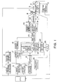
- Fig. 1 information is recorded and reproduced using a so-called optical card 1 as an optical information recording medium.
- optical card 1 At the right side of Fig. 1, the mechanical part of the apparatus is shown. A light beam 2 is focussed on the recording surface of an optical card 1.
- the position of the light beam 2 on the optical card 1 is detected by a tracking error detector 5 which detects a reflected light as a tracking error signal.
- This tracking error signal is supplied to a tracking controller 25.
- a closed circuit is formed by the tracking error detector 5, tracking controller 25, closed switch 26, and an actuator 3.
- the actuator 3 performs a so-called tracking control which controls an objective lens (not shown) so as to make the tracking error have a zero value, i.e., make the light beam always locate the center of a track.
- the actuator 3 also performs a near jump, i.e., jumping to a nearby track.
- the tracking error signal is detected by the tracking error detector 5.
- the switch 26 is opened to open the tracking control loop and stop the operation of the actuator 3.
- a linear motor 6 then moves the optical head whose motion speed is detected by sensing a scale 7 with a sensor 8.
- This apparatus constructed as above is controlled by a CPU.
- CPU supplies the apparatus with a motion command to control the apparatus.
- a position data reading unit 9 reads address data of the optical card as the position data.
- the circuit portion to be controlled by CPU will be described.
- a motion command from CPU is supplied to a target position receiving unit 13 to write the target position data in this unit 13.
- the position data written in this unit 13 is supplied to an offset adder 14.
- CPU supplies an offset addition command to this adder 14 so as to avoid a track overrun near at the periphery of the card.
- the resultant position data is then supplied to a motion direction designating unit 21 and to a motion distance calculating unit 22.
- a present position data is also supplied to the motion direction designating unit 21 and to the motion distance calculating unit 22.
- the present position data before the start of moving the optical head 4 is read from the optical card 1 by the position data reading unit 9 and supplied to a position data storage unit 15. This stored data is used as the present position data before the start of moving the optical head 4.
- the present position data after the optical head 4 moved is detected by a track traverse detecting unit 11 and motion amount detector 12, and supplied via a switch 16 to the motion direction designating unit 21 and motion distance calculating unit 22.
- the switch 16 selects data from the motion amount detector 12 and position storage unit 15.
- An output of the motion direction designating unit 21 is supplied to to a driver 32 to drive the optical head 4, and to the actuator 3 to drive the objective lens.
- An output of the motion distance calculating means 22 is supplied to a tracking on/off circuit 24 because this output determines whether the tracking control is required or not.
- the tracking on/off circuit 24 turns on or off the switch 26.
- An output of the motion distance calculating means 22 is also supplied to a far jump controller 23.
- the far jump controller 23 then generates an acceleration/deceleration pattern in accordance with the tracking motion distance, and supplies it to an optimum speed calculating unit 31.
- an error of the far jump carried out at the preceding time and stored in an error storage unit 18 is considered to generate the acceleration/deceleration pattern.
- the optimum speed calculating unit 31 is supplied with the present speed from the present speed detector 33, and sends an acceleration/deceleration signal to the driver 32 to drive a linear motor 6.
- An output of the present speed detector 33 is also supplied to the tracking on/off circuit 24 so that when the linear motor 6 is decelerated sufficiently, the tracking control starts.
- An output of the tracking on/off circuit 24 is supplied to the error detector 17 so as to use it in generating a far jump completion signal.
- the error detector 17 calculates a difference between the target position at the time of the far jump completion and the present position, the difference being supplied to the error storage unit 18 and to the far jump controller 23.
- Fig. 2 is a flow chart illustrating the operation of the apparatus shown in Fig. 1. The operation of the apparatus will be described with reference to this flow chart.
- CPU issues a motion command to write the position data of a target track in the target position receiving unit 13 (step S1).
- step S2 CPU checks whether the target track is near at the card periphery and whether an offset addition is required. If necessary, at step S3 the offset adder 14 adds an offset to the target position to avoid a track overrun.
- step S4 the data previously written in the position storage unit 15 by the position data reading unit 9 is supplied via the switch 16 to the motion direction designating unit 21 and motion distance calculating unit 22.
- step S5 the motion direction is determined, and at step S6 a motion distance is calculated.
- the far jump controller 23 judges from the magnitude of the obtained motion distance whether a far jump is required (step S7). If a far jump is required, at step S8 the far jump controller 23 determines an acceleration/deceleration pattern while considering the previous error stored in the error storage unit 18. An output of the tracking on/off unit 24 opens the switch 26 to turn off the tracking control (step S9).
- step S10 the optimum speed calculating unit 31 activates the driver 32 to drive the linear motor 6, in accordance with the determined acceleration/deceleration pattern. Acceleration continues before half the motion distance (step S11). At half the motion distance, the optimum speed calculatinq unit 31 starts a deceleration at step S12. It is checked at step S13 whether the deceleration has been made sufficiently. If sufficient, at step S14 the tracking control starts.
- a position error at the time when the far jump operation transits to the tracking control is detected by the error detector 17 at step S15, and stored at step S16 in the error storage unit 18.
- the tracking controller 25 performs the tracking control. If not, instead of an output from the position storage unit 15, the switch 16 selects an output from the motion amount detector 12 and sends it to the motion direction designating unit 21 and motion distance calculating means 22. In this manner, the motion direction designating unit 21 and motion distance calculating means 22 can know the present position which is a difference between the motion amount generated by the motion of the optical head and objective lens and the initial position data given from the position data reading unit 9.
- steps S5 to S17 are repeated until the target position is obtained.
- the far jump controller 23 judges that the operation to be carried out is not the far jump, in the motion direction designated by the motion direction designating unit 21 at step S19, the driver 32 operates to perform a near jump at step S20.
- step S21 it is judged if the target position has been obtained. If not, the operation returns to step S19. If obtained, the operation terminates.
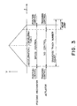
- Fig. 3 shows an example of an acceleration/deceleration pattern to be used during the speed control operation. This pattern has no constant speed area, and the acceleration area is immediately followed by the deceleration area. The time required for the conventional constant speed is not necessary, allowing to reach the target position faster.
- the feeding mechanism (linear motor for the optical head) is subject to an acceleration/deceleration control by the circuit shown in Fig. 1 during the speed control operation.
- the position of the feeding mechanism is controlled by a position controller (not shown).
- the actuator is not controlled or it is under the tracking control.
- the actuator is under the position control.
- Fig. 4 is a circuit diagram showing the structure of an embodiment of a near jump controller for controlling an optical head to jump to a nearby track according to the present invention.
- Fig. 5 is a detailed circuit diagram showing the structure of the track traverse detector in the circuit shown in Fig. 4.
- Figs. 6A and 6B are timing charts showing signal waveforms at various circuit portions shown in Fig. 4.
- reference numeral 107 represents an optical information recording medium.
- a light beam radiated through an objective lens 106 is focussed on the optical card 107, and the reflected light is applied to an optical detector 101 to form a tracking error signal.
- This tracking error signal is amplified by an amplifier 102 and supplied via a switch SW101 to a tracking controller 104 to drive a tracking coil 105 for driving the objective lens 106.
- the tracking error signal is also supplied to a track traverse detector 103 the details of which will be later described with Fig. 5.
- the track traverse detector 103 shapes the tracking error signal into a rectangular waveform to generate a track traverse detecting signal.
- This track traverse detecting signal is supplied to one input terminal of an exclusive OR EXOR100. Supplied to the other input terminal of EXOR100 is a direction control signal which takes an L level when the objective lens is moved in the forward direction and an H level when it is moved in the backward direction.
- the direction control signal is also used for opening and closing a switch SW103.
- the switch SW103 opens to supply the positive power source voltage +V to the left contact of the switch SW102 as viewed in Fig. 4 via resistors R101 and R102.
- the switch SW103 closes to supply the negative power source voltage -V to the left contact of the switch SW102 via the resistor R102.
- a signal at the Q output terminal of a flip-flop FF100 is used for opening and closing the switch SW101.
- This signal of an H level closes the switch SW101 to always maintain the light beam at the center of a track, and the signal of an L level opens the switch SW101.
- a signal at an inverted Q output terminal of the flip-flop FF100 as well as an output from EXOR100 is supplied to an AND gate AND100 whose output is used for opening and closing the switch SW102.
- a voltage corresponding to the state of the switch SW103 is supplied to the tracking controller 104 via a conversion circuit made of a parallel circuit of a resistor R104 and a serially connected resistor R105 and capacitor C100.
- the tracking controller 104 flows a current to the tracking coil 105 to start moving the objective lens 106.
- the tracking controller 104 receives a voltage signal of an inverted polarity and flows a damping current to the tracking coil 105.
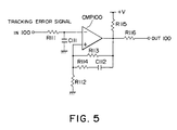
- Fig. 5 shows the detailed structure of the track traverse detector 103 shown in Fig. 4.
- the tracking error signal applied to an input terminal IN100 is supplied to the inverting terminal of a comparator CMP100 via an integrator made of a resistor R111 and capacitor C111.
- a reference signal Vref is applied to the non-inverting input terminal of the comparator CMP100.
- the tracking error signal is compared with the reference signal, and the comparison result is outputted via a resistor R116 to an output terminal OUT100.
- This reference voltage Vref is a voltage divided by a serial circuit made of resistors R115, R113, and R112.
- the resistor R113 is a feedback element connected between the non-inverting input terminal and output terminal of the comparator CMP100.
- the reference voltage Vref changes with an output voltage of the comparator CMP100.
- a serial circuit of a resistor R114 and capacitor C112 is also connected to add an offset to an output of the comparator CMP100.
- Fig. 6(a) and (b) shows signal waveforms at various circuit portions of Fig. 4 during the forward jump and backward jump operations. The operation of the circuit of Fig. 4 will be described with reference to these waveforms shown in Fig. 6(a) and (b).
- the direction control signal is set to an L level for the forward direction jump.
- the switch SW103 opens, and so the positive voltage is applied via the resistors R101 and R102 to the left contact of the switch SW102.
- a track jump command of an L level is issued at time t11 and supplied to an inverted reset terminal R of the flip-flop FF100. Therefore, the Q output of the flip-flop FF100 takes an L level to open the switch SW101 and stop the control of making the light beam follow the center of a track.
- the inverted Q output of the flip-flop FF100 takes an H level to close the switch SW102 and supply a positive voltage to the converter circuit made of the resistors R104, R105 and capacitor C100. Accordingly, a drive current shown in Fig. 6(a) flows in the tracking coil 105 to start moving the objective lens 106 in the forward direction.
- the tracking error signal changes from a zero level to a negative level and from the zero level to a positive level.
- the track traverse detecting signal takes an L level. Therefore, both the inputs to EXOR100 are L level, and the output is L level. With an L level of the output of EXOR100, the input conditions of the AND gate AND100 are negated. Therefore, the AND gate AND100 supplies an L level signal to the switch SW102 to open it.
- the positive voltage having been applied to the conversion circuit disappears at once so that a current in the opposite direction will flow through the tracking coil 105 to provide a fast damping.
- This damping is carried out at time t 12 shown in Fig. 6(a).
- the track traverse detecting signal takes an H level.
- EXOR100 outputs an H level signal.
- the rising edge of this H level signal is applied to a clock terminal of the flip-flop FF100 so that the Q output of the flip-flop FF100 takes an H level to close the switch SW101 and lock the objective lens 106 at that position.
- the inverted Q output of the flip-flop FF100 takes an L level, and so the input conditions of the AND gate AND100 are negated to supply an L level signal to the switch SW102.
- the direction control signal is set to an H level for the backward direction jump. Therefore, the switch SW103 closes, and so the negative voltage is applied via the resistor R102 to the left contact of the switch SW102.
- the switch SW102 closes, the direction of the current flowing through the tracking coil 105 becomes opposite to that during the forward direction jump.
- the tracking error signal changes in the opposite direction to that shown in Fig. 6(a). The operation is similar to that during the forward direction jump except that the input conditions to EXOR100 are reversed.
- Fig. 7 is a circuit diagram showing another embodiment of the present invention.
- IN201 to IN203 represent input terminals.
- the input terminal IN201 is supplied with a tracking error signal which is detected with a detector assembled with an optical head (not shown).
- the input terminal IN202 is supplied with a tracking control signal, and the input terminal IN203 is supplied with a direction control signal.
- the tracking error signal applied to the input terminal IN201 is an analog signal whose polarity becomes positive and negative in response to a track traverse of the optical head.
- the tracking error signal is supplied to the inverting input terminal of a comparator CMP200 via an integrator made of a resistor R201 and capacitor C201.
- Connected between the non-inverting input terminal and output terminal of the comparator CMP200 are a first feedback element constructed of a resistor R203, a second feedback element constructed of a serially connected resistor R204 and capacitor C202, and a third feedback element constructed of a serially connected resistor R205 and switch SW201.
- the first and second feedback elements are always connected, and the third feedback element is connected or disconnected by the switch SW201 to change the feedback amount which becomes large when the switch SW201 is closed, and small when it is opened.
- the tracking control signal applied to the input terminal IN202 is an on/off signal which is directly supplied to the switches SW201 and SW202. These switches close during the on-tracking, and open during the off-tracking.
- the switch SW201 closes, the resistor R205 is connected between the non-inverting input terminal and output terminal of the comparator CMP200 to increase the feedback amount between these terminals.
- the switch SW202 closes, the interconnection point between the resistors R208 and R209 is grounded via the switch SW202, so that the direction control signal applied from the input terminal IN203 via the resistor R209 does not reach the non-inverting input terminal of the comparator CMP200.
- the direction control signal applied to the input terminal IN203 is an on/off signal which is directly supplied to the switch SW203.
- the switch SW203 opens for the forward direction, and closes for the backward direction.
- the direction control signal is applied to one input terminal of an exclusive OR EXOR200, and the other input terminal is supplied with an output signal from the comparator CMP200.
- the result of the logical operation by EXOR200 is used in generating the track traverse detecting signal.
- the tracking error signal from the input terminal IN201 is applied to the inverting input terminal of the comparator CMP200.
- the non-inverting input terminal is grounded via a resistor R202, and connected via the resistors R208 and R209 to the interconnection point between a resistor 210 and switch SW203.
- the switch SW203 opens and closes in response to the on and off of the direction control signal.
- the switch SW203 opens to supply a positive voltage +V from a positive power source to the non-inverting input terminal of the comparator CMP200 via the resistors R208 and R209.
- the switch SW203 closes to supply a negative voltage -V from a negative power source to the non-inverting input terminal of the comparator CMP200 via the resistors R208 and R209.
- An output terminal of the comparator CMP200 is connected to the positive power source +V via a resistor R206, and to the other input terminal of EXOR200 via an integrator made of a resistor R207 and capacitor C203.
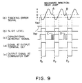
- Figs. 8 to 10 show waveforms at various circuit portions of the circuit shown in Fig. 7 during various operations.
- Fig. 8 is for the forward direction near jump
- Fig. 9 is for the backward direction near jump
- Fig. 10 is for the far jump, a comparison with a conventional circuit operation being provided.
- waveforms indicated at (a) are of the tracking error signal
- waveforms indicated at (b) are of a slice signal for slicing the tracking error signal
- waveforms indicated at (d) are of the signal at an output terminal OUT
- waveforms indicated at (e) are of the output signal of the comparator CMP200.
- Three operation modes including a forward direction near jump mode, backward direction near jump mode, and far jump mode, are selected by the on/off operations of the switches SW201 to SW203.
- the forward near jump mode all the switches SW201, SW202, and SW203 are turned off.
- the backward near jump mode the switches SW201 and SW202 are turned off and the switch SW203 is turned on.
- the tracking control is performed to correctly align the optical head on a track.
- the far jump mode the switches SW201 and SW202 are turned on (the switch SW203 may be turned on or off).
- the far jump mode it is sufficient if the number of tracks jumped by the optical head 4 can be correctly known, and it is not important to check whether the optical head is correctly on a track.
- the first feedback element made of the resistor R203 and the second feedback element made of the serially connected resistor R204 and capacitor C202 are inserted between the non-inverting input terminal and output terminal of the comparator CMP200.
- the non-inverting input terminal is connected to the positive power source +V via the resistors R208 to R210.
- the potential or slice level at the non-inverting input terminal of the comparator CMP200 is a voltage obtained by dividing the positive voltage +V by the serially connected resistors R202, R208, R209, and R210. This voltage is a positive value Vs1 as indicated at (b) of Fig. 8.
- the level of the tracking error signal at the input terminal IN201 is checked by this positive high voltage. Therefore, the output signal of the comparator CMP200 is a correct rectangle as indicated at (e) of Fig. 8.
- the waveforms indicated at (e) and (d) of Fig. 8 are compared with a conventional track traverse detected signal indicated at (c) of Fig. 8, it can be seen that there is a distinct difference therebetween.
- the waveform indicated at (d) of Fig. 8 is a correct rectangle, without having a pulsating signal C at the disturbed area A of the signal near the zero level indicated at (a) of Fig. 8 and a short duration rectangle D at the shoulder B indicated at (a) of Fig. 8.
- the switches SW201 and SW202 are off and the switch SW203 is on. Therefore, a different point from the positive direction near jump is that the negative power source -V is supplied to the non-inverting input terminal of the comparator CMP200 via the switch SW203 and resistors R208 and R209.
- the slice level of the comparator CMP200 is a negative value Vs2.
- the level of the tracking error signal is checked using this slice level.
- a rectangular signal indicated at (e) of Fig. 9 is generated accordingly.
- the signal at the output terminal OUT200 is also a rectangular signal.
- the waveform indicated at (d) of Fig. 9 is a correct rectangle, without having a pulsating signal C at the disturbed area A of the signal near the zero level indicated at (a) of Fig. 9 and a short duration rectangle D at the shoulder B indicated at (a) of Fig. 9.
- the switches SW201 and SW202 are on. Therefore, the first to third feedback elements are connected between the non-inverting input terminal and output terminal of the comparator CMP200, providing a large feedback amount. Different from the near jump, the comparator CMP200 is not supplied with a voltage via the resistors R208 and R209, and so the potential at the non-inverting input terminal changes with a signal at the output terminal.
- the waveform indicated at (d) of Fig. 10 is a correct rectangle, without having a pulsating signal C at the disturbed area A of the signal near the zero level indicated at (a) of Fig. 10 and a short duration rectangle D at the shoulder B indicated at (a) of Fig. 10.
- the rectangular signal indicated at (d) of Fig. 10 is not so precise as the falling edge Po in the negative direction or the rising edge Po in the positive direction of the rectangular signal in the near jump mode.
- the far jump control does not pose any problem even if it is coarse, because the near jump control is executed thereafter.
- the track traverse detecting signal can be obtained from the tracking error signal without being adversely affected by noises contained in the tracking error signal.
Description
Claims (4)
- An information recording and reproducing apparatus for an optical information recording medium (1) for recording and reproducing information to and from the optical information recording medium (1) by scanning each track of the medium with a light beam (2) from an optical head (4), the light beam (2) being moved from a first position to a second position on the medium (1) through a combination of a far jump driving the optical head and near jump driving an objective lens assembled with the optical head, said apparatus comprising:a position reading means (9) for scanning said medium to read present address information;a position storage means (15) for storing said present address information;a traverse signal generating means (11) for generating a track traverse detecting signal by detecting that said light beam (2) traverses said track on said medium;a motion amount detecting means (12) being reset at the start of the operation of the information recording and reproducing apparatus, for receiving an output of said traverse signal generating means (11) and detecting a motion amount of said optical head (4) over said medium;a switching means (16) for selecting an output of said position storage means (15) when an output of said motion amount detecting means (12) is zero, and selecting an output of said motion amount detecting means (12) when an output of said motion amount detecting means (12) is not zero;a target position receiving means (13) responsive to a next information recording and reproducing command for said medium for receiving a target position;a direction designating means (21) for determining a motion direction by comparing said target position reveiced by said target position reveiving means (13) with one of said present positions stored in said position storage means (15) and said motion amount detected by said motion mount detecting means (12);a motion distance calculating means (22) for calculating a motion distance by comparing said target position received by said target position receiving means (13) with said present position stored in said position storing means (15), and calculating said motion distance after the motion start by comparing said target position with said motion amount;an on/off controlling means (24) for a tracking control for performing a near jump scan when said motion distance calculated by said motion distance calculating means (22) is smaller than a predetermined value, and performing a far jump scan when said motion distance is larger than said predetermined value;a motion speed controlling means (6, 7, 8, 31, 32, 33) responsive to a selection of said far jump by said on/off controlling means (24), for controlling to move said optical head (4) in the motion direction designated by said direction designating means (21), by half said motion distance calculated by said motion distance calculating means (22) in an acceleration mode, and by the remaining half of said motion distance in a deceleration mode; anda driving means (32) for moving said optical head (4) in accordance with outputs from said direction designating means (21) and said motion speed controlling means.
- The information recording and reproducing apparatus according to claim 1, comprising:an error detecting means (17) for detecting an error representing a difference between said target position after the completion of said far jump and said present position stored in said position storage means (15); andan error storage means (18) for storing said error detected by said error detecting means (17),wherein the operation of said motion speed controlling means (6, 7, 8, 31, 32, 33) is controlled in accordance with said error stored in said error storage means (18).
- The information recording and reproducing apparatus according to claim 1, wherein said motion speed controlling means (6, 7, 8, 31, 32, 33) includes:a present speed detecting means (33) for detecting a motion speed of said optical head (4);an optimum speed calculating means (31) for calculating a speed for accelerating and decelerating said optical head (4) in accordance with said speed detected by said present speed detecting means (33); anda driving means (6, 32) for moving said optical head (4) in accordance with an output of said optimum speed calculating means (31).
- The information recording and reproducing apparatus according to claim 3, wherein said on/off controlling means (24) turns on a tracking control when an output of said present speed detecting means (33) becomes smaller than a predetermined value.
Priority Applications (2)
| Application Number | Priority Date | Filing Date | Title |
|---|---|---|---|
| EP97114961A EP0813191B1 (en) | 1991-10-09 | 1992-10-08 | Circuit for generating a track traverse detecting signal in an information recording and reproducing apparatus for an optical information recording medium |
| EP97114960A EP0813190B1 (en) | 1991-10-09 | 1992-10-08 | Jump controller for an optical information recording and reproducing apparatus |
Applications Claiming Priority (6)
| Application Number | Priority Date | Filing Date | Title |
|---|---|---|---|
| JP262283/91 | 1991-10-09 | ||
| JP26228391A JP2925807B2 (en) | 1991-10-09 | 1991-10-09 | Track crossing detection signal forming circuit for optical information recording medium |
| JP29454491A JPH05135377A (en) | 1991-11-11 | 1991-11-11 | Jump controller to proximity track for optical head |
| JP294544/91 | 1991-11-11 | ||
| JP316521/91 | 1991-11-29 | ||
| JP31652191A JPH05151586A (en) | 1991-11-29 | 1991-11-29 | Information recording and reproducing device for optical information recording medium |
Related Child Applications (2)
| Application Number | Title | Priority Date | Filing Date |
|---|---|---|---|
| EP97114960A Division EP0813190B1 (en) | 1991-10-09 | 1992-10-08 | Jump controller for an optical information recording and reproducing apparatus |
| EP97114961A Division EP0813191B1 (en) | 1991-10-09 | 1992-10-08 | Circuit for generating a track traverse detecting signal in an information recording and reproducing apparatus for an optical information recording medium |
Publications (3)
| Publication Number | Publication Date |
|---|---|
| EP0536737A2 EP0536737A2 (en) | 1993-04-14 |
| EP0536737A3 EP0536737A3 (en) | 1993-09-01 |
| EP0536737B1 true EP0536737B1 (en) | 1998-03-11 |
Family
ID=27335113
Family Applications (3)
| Application Number | Title | Priority Date | Filing Date |
|---|---|---|---|
| EP97114960A Expired - Lifetime EP0813190B1 (en) | 1991-10-09 | 1992-10-08 | Jump controller for an optical information recording and reproducing apparatus |
| EP97114961A Expired - Lifetime EP0813191B1 (en) | 1991-10-09 | 1992-10-08 | Circuit for generating a track traverse detecting signal in an information recording and reproducing apparatus for an optical information recording medium |
| EP92117178A Expired - Lifetime EP0536737B1 (en) | 1991-10-09 | 1992-10-08 | Information recording/reproducing apparatus for optical information recording medium |
Family Applications Before (2)
| Application Number | Title | Priority Date | Filing Date |
|---|---|---|---|
| EP97114960A Expired - Lifetime EP0813190B1 (en) | 1991-10-09 | 1992-10-08 | Jump controller for an optical information recording and reproducing apparatus |
| EP97114961A Expired - Lifetime EP0813191B1 (en) | 1991-10-09 | 1992-10-08 | Circuit for generating a track traverse detecting signal in an information recording and reproducing apparatus for an optical information recording medium |
Country Status (4)
| Country | Link |
|---|---|
| US (3) | US5309417A (en) |
| EP (3) | EP0813190B1 (en) |
| CA (1) | CA2080057C (en) |
| DE (3) | DE69230571T2 (en) |
Families Citing this family (16)
| Publication number | Priority date | Publication date | Assignee | Title |
|---|---|---|---|---|
| US5566141A (en) * | 1993-04-13 | 1996-10-15 | Matsushita Electric Industrial Co., Ltd. | Track retrieving method for making a light beam jump and scan from one track to another |
| JP2802479B2 (en) * | 1994-08-09 | 1998-09-24 | 富士通株式会社 | Optical disk drive |
| KR0135787B1 (en) | 1995-05-13 | 1998-05-15 | 김광호 | Disk calibrating method for cd-rom |
| KR100211207B1 (en) * | 1995-12-27 | 1999-07-15 | 윤종용 | Track jump stabilization method of disk drive |
| KR19980021850A (en) * | 1996-09-19 | 1998-06-25 | 구자홍 | Fast Access Method of Optical Disc Player |
| JP3484039B2 (en) * | 1997-03-14 | 2004-01-06 | 株式会社東芝 | Disk unit |
| US6024750A (en) * | 1997-08-14 | 2000-02-15 | United States Surgical | Ultrasonic curved blade |
| JP2001518675A (en) * | 1997-09-26 | 2001-10-16 | テーウー エレクトロニクス カンパニー リミテッド | Method and apparatus for controlling track search in an optical disc system |
| US6169382B1 (en) | 1998-07-02 | 2001-01-02 | Seagate Technology Llc | Adapting seek velocity profile to destination track location |
| US6750900B1 (en) * | 1998-07-23 | 2004-06-15 | Eastman Kodak Company | Method and apparatus for computing motion tracking parameters |
| TW464846B (en) * | 2000-02-01 | 2001-11-21 | Via Tech Inc | Method and device to resolve the turn back problem of the seeking control of optical disk driver |
| US20030074285A1 (en) * | 2001-03-23 | 2003-04-17 | Restaurant Services, Inc. | System, method and computer program product for translating sales data in a supply chain management framework |
| KR20030005380A (en) * | 2001-03-29 | 2003-01-17 | 소니 가부시끼 가이샤 | Disk drive apparatus and information reading method |
| TW200527418A (en) * | 2004-02-03 | 2005-08-16 | Mediatek Inc | Method and device determining tracking error signal polarity of target track while CD drive skips to end track |
| US7420348B2 (en) * | 2005-02-22 | 2008-09-02 | Matsushita Electric Industrial Co., Ltd. | Drive apparatus |
| TW201003644A (en) * | 2008-07-14 | 2010-01-16 | Quanta Storage Inc | Reading method and device for optical disk drives |
Family Cites Families (24)
| Publication number | Priority date | Publication date | Assignee | Title |
|---|---|---|---|---|
| JPS6215864Y2 (en) * | 1980-08-04 | 1987-04-22 | ||
| DE3280460T2 (en) * | 1981-10-28 | 1995-06-14 | Discovision Ass | Method for reproducing information from a selected track on a recording disk. |
| JPS58166567A (en) * | 1982-03-26 | 1983-10-01 | Matsushita Electric Ind Co Ltd | Retrieving device of information track |
| JPS5984379A (en) * | 1982-11-08 | 1984-05-16 | Nec Corp | Track access device of disklike record carrier |
| JPS59152568A (en) * | 1983-02-21 | 1984-08-31 | Toshiba Corp | Optical disk record reproducer |
| JPS59198570A (en) * | 1983-04-22 | 1984-11-10 | Asahi Optical Co Ltd | High speed search system in video disc reproducing device |
| JPS61977A (en) * | 1984-06-13 | 1986-01-06 | Pioneer Electronic Corp | Tracking servo device |
| KR910003458B1 (en) * | 1986-12-02 | 1991-05-31 | 미쓰비시뎅끼 가부시끼가이샤 | Operating apparatus of optical disk |
| US5184338A (en) * | 1987-06-25 | 1993-02-02 | Mitsubishi Denki Kabushiki Kaisha | Optical disc system with improved track jumping operation |
| EP0332708B1 (en) * | 1987-08-29 | 1994-01-12 | Fujitsu Limited | Methods of accessing an optical recording track |
| JP2563383B2 (en) * | 1987-10-23 | 1996-12-11 | 松下電器産業株式会社 | Recording and playback device |
| JP2632969B2 (en) * | 1988-10-11 | 1997-07-23 | キヤノン株式会社 | Optical information recording / reproducing device |
| JP2581784B2 (en) * | 1988-11-30 | 1997-02-12 | 富士通株式会社 | Optical disk drive |
| JP2646130B2 (en) * | 1989-03-13 | 1997-08-25 | パイオニア株式会社 | Track jump drive |
| JPH02263367A (en) * | 1989-04-04 | 1990-10-26 | Pioneer Electron Corp | Pickup driving device for disk player |
| JPH0323571A (en) * | 1989-06-21 | 1991-01-31 | Nec Corp | Track access control system for disk device |
| JPH0325765A (en) * | 1989-06-23 | 1991-02-04 | Mitsubishi Electric Corp | Disk device |
| US5301174A (en) * | 1989-07-14 | 1994-04-05 | Sharp Kabushiki Kaisha | Optical disk recording and reproducing apparatus |
| JP2685909B2 (en) * | 1989-07-14 | 1997-12-08 | シャープ株式会社 | Access control device in optical disk device |
| JP2760077B2 (en) * | 1989-08-29 | 1998-05-28 | ソニー株式会社 | Optical disk seek circuit |
| JPH03276466A (en) * | 1990-03-26 | 1991-12-06 | Ricoh Co Ltd | Information reproducing device |
| JP2656371B2 (en) * | 1990-06-26 | 1997-09-24 | 富士通株式会社 | Optical disk drive |
| US5199017A (en) * | 1991-09-11 | 1993-03-30 | International Business Machines Corporation | Optical disk drive and method for counting the number of tracks on an optical disk |
| KR920006926A (en) * | 1990-09-29 | 1992-04-28 | 정용문 | Track eccentricity correction method of optical disk drive device and device therefor |
-
1992
- 1992-10-06 US US07/957,407 patent/US5309417A/en not_active Expired - Fee Related
- 1992-10-07 CA CA002080057A patent/CA2080057C/en not_active Expired - Fee Related
- 1992-10-08 DE DE69230571T patent/DE69230571T2/en not_active Expired - Fee Related
- 1992-10-08 EP EP97114960A patent/EP0813190B1/en not_active Expired - Lifetime
- 1992-10-08 EP EP97114961A patent/EP0813191B1/en not_active Expired - Lifetime
- 1992-10-08 DE DE69232506T patent/DE69232506T2/en not_active Expired - Fee Related
- 1992-10-08 DE DE69224693T patent/DE69224693T2/en not_active Expired - Fee Related
- 1992-10-08 EP EP92117178A patent/EP0536737B1/en not_active Expired - Lifetime
-
1994
- 1994-01-10 US US08/179,484 patent/US5477513A/en not_active Expired - Fee Related
-
1995
- 1995-06-07 US US08/479,951 patent/US5581527A/en not_active Expired - Fee Related
Also Published As
| Publication number | Publication date |
|---|---|
| DE69230571T2 (en) | 2000-08-17 |
| DE69224693T2 (en) | 1998-07-02 |
| US5477513A (en) | 1995-12-19 |
| DE69232506D1 (en) | 2002-04-25 |
| DE69232506T2 (en) | 2003-01-02 |
| US5309417A (en) | 1994-05-03 |
| EP0813191B1 (en) | 2000-01-12 |
| CA2080057C (en) | 1997-05-20 |
| EP0813191A2 (en) | 1997-12-17 |
| EP0536737A2 (en) | 1993-04-14 |
| CA2080057A1 (en) | 1993-04-10 |
| EP0536737A3 (en) | 1993-09-01 |
| EP0813191A3 (en) | 1998-02-11 |
| DE69230571D1 (en) | 2000-02-17 |
| EP0813190A2 (en) | 1997-12-17 |
| EP0813190B1 (en) | 2002-03-20 |
| US5581527A (en) | 1996-12-03 |
| DE69224693D1 (en) | 1998-04-16 |
| EP0813190A3 (en) | 1998-02-11 |
Similar Documents
| Publication | Publication Date | Title |
|---|---|---|
| EP0536737B1 (en) | Information recording/reproducing apparatus for optical information recording medium | |
| US5063549A (en) | Optical disk apparatus | |
| US4736353A (en) | Disc accessing using coarse and fine actuators with the fine actuator locked during coarse actuator movement | |
| US5003524A (en) | Optical disk drive with an accurately positioned objective lens | |
| US4837757A (en) | Optical recording/reproducing device | |
| US4835752A (en) | Device for driving and controlling optical head for use in optical disk system | |
| US5077716A (en) | Optical recording and reproducing system having an accurate high-speed optical head positioning apparatus | |
| EP0424980B1 (en) | Optical disk drive device and information storage device | |
| JPH09305984A (en) | Optical memory device | |
| US5021898A (en) | Head positioning control method and apparatus | |
| EP0617416B1 (en) | Information processing apparatus | |
| EP0322841B1 (en) | Optical disk apparatus | |
| EP0441969B1 (en) | Seek circuit of optical disk | |
| US6804176B1 (en) | Apparatus and method for performing track search | |
| CA2137220C (en) | Track seek method and device for use with an optical information recording and reproducing apparatus | |
| JPH04177678A (en) | Disk driver | |
| US6674694B1 (en) | Light-pickup device applied to a recording and/or reproduction device for an optical disk inluding a detection circuit that generates a focus zero cross signal | |
| JP2919458B2 (en) | Apparatus and method for automatically adjusting thread loop gain in optical disk drive | |
| JPH09167357A (en) | Track jump controller for optical recording and reproducing device | |
| JP2684732B2 (en) | Optical disk seek device | |
| JPH0821209B2 (en) | Optical disk drive | |
| JPH0755718Y2 (en) | Optical disk seek device | |
| JP2553542B2 (en) | Information recording disk playback device | |
| JP2724002B2 (en) | Optical card device | |
| JPH05189898A (en) | Disc player |
Legal Events
| Date | Code | Title | Description |
|---|---|---|---|
| PUAI | Public reference made under article 153(3) epc to a published international application that has entered the european phase |
Free format text: ORIGINAL CODE: 0009012 |
|
| 17P | Request for examination filed |
Effective date: 19921031 |
|
| AK | Designated contracting states |
Kind code of ref document: A2 Designated state(s): DE FR GB IT |
|
| PUAL | Search report despatched |
Free format text: ORIGINAL CODE: 0009013 |
|
| AK | Designated contracting states |
Kind code of ref document: A3 Designated state(s): DE FR GB IT |
|
| 17Q | First examination report despatched |
Effective date: 19960131 |
|
| GRAG | Despatch of communication of intention to grant |
Free format text: ORIGINAL CODE: EPIDOS AGRA |
|
| GRAG | Despatch of communication of intention to grant |
Free format text: ORIGINAL CODE: EPIDOS AGRA |
|
| GRAH | Despatch of communication of intention to grant a patent |
Free format text: ORIGINAL CODE: EPIDOS IGRA |
|
| GRAH | Despatch of communication of intention to grant a patent |
Free format text: ORIGINAL CODE: EPIDOS IGRA |
|
| GRAA | (expected) grant |
Free format text: ORIGINAL CODE: 0009210 |
|
| AK | Designated contracting states |
Kind code of ref document: B1 Designated state(s): DE FR GB IT |
|
| DX | Miscellaneous (deleted) | ||
| PG25 | Lapsed in a contracting state [announced via postgrant information from national office to epo] |
Ref country code: IT Free format text: LAPSE BECAUSE OF FAILURE TO SUBMIT A TRANSLATION OF THE DESCRIPTION OR TO PAY THE FEE WITHIN THE PRESCRIBED TIME-LIMIT;WARNING: LAPSES OF ITALIAN PATENTS WITH EFFECTIVE DATE BEFORE 2007 MAY HAVE OCCURRED AT ANY TIME BEFORE 2007. THE CORRECT EFFECTIVE DATE MAY BE DIFFERENT FROM THE ONE RECORDED. Effective date: 19980311 |
|
| REF | Corresponds to: |
Ref document number: 69224693 Country of ref document: DE Date of ref document: 19980416 |
|
| ET | Fr: translation filed | ||
| PLBE | No opposition filed within time limit |
Free format text: ORIGINAL CODE: 0009261 |
|
| STAA | Information on the status of an ep patent application or granted ep patent |
Free format text: STATUS: NO OPPOSITION FILED WITHIN TIME LIMIT |
|
| 26N | No opposition filed | ||
| REG | Reference to a national code |
Ref country code: GB Ref legal event code: IF02 |
|
| PGFP | Annual fee paid to national office [announced via postgrant information from national office to epo] |
Ref country code: GB Payment date: 20051005 Year of fee payment: 14 |
|
| PGFP | Annual fee paid to national office [announced via postgrant information from national office to epo] |
Ref country code: FR Payment date: 20051026 Year of fee payment: 14 |
|
| PGFP | Annual fee paid to national office [announced via postgrant information from national office to epo] |
Ref country code: DE Payment date: 20051227 Year of fee payment: 14 |
|
| PG25 | Lapsed in a contracting state [announced via postgrant information from national office to epo] |
Ref country code: DE Free format text: LAPSE BECAUSE OF NON-PAYMENT OF DUE FEES Effective date: 20070501 |
|
| GBPC | Gb: european patent ceased through non-payment of renewal fee |
Effective date: 20061008 |
|
| REG | Reference to a national code |
Ref country code: FR Ref legal event code: ST Effective date: 20070629 |
|
| PG25 | Lapsed in a contracting state [announced via postgrant information from national office to epo] |
Ref country code: GB Free format text: LAPSE BECAUSE OF NON-PAYMENT OF DUE FEES Effective date: 20061008 |
|
| PG25 | Lapsed in a contracting state [announced via postgrant information from national office to epo] |
Ref country code: FR Free format text: LAPSE BECAUSE OF NON-PAYMENT OF DUE FEES Effective date: 20061031 |