EP0536394B1 - Method of producing polycrystalline silicon rods for semiconductors and thermal decomposition furnace therefor - Google Patents
Method of producing polycrystalline silicon rods for semiconductors and thermal decomposition furnace therefor Download PDFInfo
- Publication number
- EP0536394B1 EP0536394B1 EP90909847A EP90909847A EP0536394B1 EP 0536394 B1 EP0536394 B1 EP 0536394B1 EP 90909847 A EP90909847 A EP 90909847A EP 90909847 A EP90909847 A EP 90909847A EP 0536394 B1 EP0536394 B1 EP 0536394B1
- Authority
- EP
- European Patent Office
- Prior art keywords
- silicon
- thermal decomposition
- filaments
- shield
- rods
- Prior art date
- Legal status (The legal status is an assumption and is not a legal conclusion. Google has not performed a legal analysis and makes no representation as to the accuracy of the status listed.)
- Expired - Lifetime
Links
- 238000005979 thermal decomposition reaction Methods 0.000 title claims abstract description 50
- 229910021420 polycrystalline silicon Inorganic materials 0.000 title claims abstract description 19
- 238000000034 method Methods 0.000 title abstract description 21
- 239000004065 semiconductor Substances 0.000 title abstract description 3
- XUIMIQQOPSSXEZ-UHFFFAOYSA-N Silicon Chemical compound [Si] XUIMIQQOPSSXEZ-UHFFFAOYSA-N 0.000 claims abstract description 98
- 229910052710 silicon Inorganic materials 0.000 claims abstract description 98
- 239000010703 silicon Substances 0.000 claims abstract description 98
- BLRPTPMANUNPDV-UHFFFAOYSA-N Silane Chemical compound [SiH4] BLRPTPMANUNPDV-UHFFFAOYSA-N 0.000 claims abstract description 18
- 238000004519 manufacturing process Methods 0.000 claims description 19
- 238000001816 cooling Methods 0.000 claims description 7
- 230000007246 mechanism Effects 0.000 claims description 5
- 238000005192 partition Methods 0.000 abstract description 4
- 239000007789 gas Substances 0.000 description 27
- 230000008569 process Effects 0.000 description 11
- 239000000463 material Substances 0.000 description 8
- 238000006243 chemical reaction Methods 0.000 description 7
- 239000013078 crystal Substances 0.000 description 7
- VEXZGXHMUGYJMC-UHFFFAOYSA-M Chloride anion Chemical compound [Cl-] VEXZGXHMUGYJMC-UHFFFAOYSA-M 0.000 description 5
- 238000000354 decomposition reaction Methods 0.000 description 5
- 230000000694 effects Effects 0.000 description 5
- 239000007858 starting material Substances 0.000 description 5
- 230000009467 reduction Effects 0.000 description 4
- 150000004756 silanes Chemical class 0.000 description 4
- 230000015572 biosynthetic process Effects 0.000 description 3
- 239000007788 liquid Substances 0.000 description 3
- 239000000047 product Substances 0.000 description 3
- 238000000197 pyrolysis Methods 0.000 description 3
- 230000005855 radiation Effects 0.000 description 3
- 238000010276 construction Methods 0.000 description 2
- 238000000151 deposition Methods 0.000 description 2
- 238000010348 incorporation Methods 0.000 description 2
- 238000002844 melting Methods 0.000 description 2
- 230000008018 melting Effects 0.000 description 2
- 238000002156 mixing Methods 0.000 description 2
- 230000036632 reaction speed Effects 0.000 description 2
- 229910000077 silane Inorganic materials 0.000 description 2
- 238000002231 Czochralski process Methods 0.000 description 1
- UFHFLCQGNIYNRP-UHFFFAOYSA-N Hydrogen Chemical compound [H][H] UFHFLCQGNIYNRP-UHFFFAOYSA-N 0.000 description 1
- 230000009471 action Effects 0.000 description 1
- 238000007796 conventional method Methods 0.000 description 1
- 239000000498 cooling water Substances 0.000 description 1
- 238000002425 crystallisation Methods 0.000 description 1
- 230000008025 crystallization Effects 0.000 description 1
- 230000003247 decreasing effect Effects 0.000 description 1
- 230000008021 deposition Effects 0.000 description 1
- 230000005611 electricity Effects 0.000 description 1
- 239000012467 final product Substances 0.000 description 1
- 238000010438 heat treatment Methods 0.000 description 1
- 239000001257 hydrogen Substances 0.000 description 1
- 229910052739 hydrogen Inorganic materials 0.000 description 1
- 238000002955 isolation Methods 0.000 description 1
- 238000005259 measurement Methods 0.000 description 1
- 239000002184 metal Substances 0.000 description 1
- 239000000843 powder Substances 0.000 description 1
- 239000010453 quartz Substances 0.000 description 1
- VYPSYNLAJGMNEJ-UHFFFAOYSA-N silicon dioxide Inorganic materials O=[Si]=O VYPSYNLAJGMNEJ-UHFFFAOYSA-N 0.000 description 1
- 239000007787 solid Substances 0.000 description 1
- ZDHXKXAHOVTTAH-UHFFFAOYSA-N trichlorosilane Chemical compound Cl[SiH](Cl)Cl ZDHXKXAHOVTTAH-UHFFFAOYSA-N 0.000 description 1
- 239000005052 trichlorosilane Substances 0.000 description 1
- 238000004857 zone melting Methods 0.000 description 1
Images

Classifications
-
- C—CHEMISTRY; METALLURGY
- C23—COATING METALLIC MATERIAL; COATING MATERIAL WITH METALLIC MATERIAL; CHEMICAL SURFACE TREATMENT; DIFFUSION TREATMENT OF METALLIC MATERIAL; COATING BY VACUUM EVAPORATION, BY SPUTTERING, BY ION IMPLANTATION OR BY CHEMICAL VAPOUR DEPOSITION, IN GENERAL; INHIBITING CORROSION OF METALLIC MATERIAL OR INCRUSTATION IN GENERAL
- C23C—COATING METALLIC MATERIAL; COATING MATERIAL WITH METALLIC MATERIAL; SURFACE TREATMENT OF METALLIC MATERIAL BY DIFFUSION INTO THE SURFACE, BY CHEMICAL CONVERSION OR SUBSTITUTION; COATING BY VACUUM EVAPORATION, BY SPUTTERING, BY ION IMPLANTATION OR BY CHEMICAL VAPOUR DEPOSITION, IN GENERAL
- C23C16/00—Chemical coating by decomposition of gaseous compounds, without leaving reaction products of surface material in the coating, i.e. chemical vapour deposition [CVD] processes
- C23C16/44—Chemical coating by decomposition of gaseous compounds, without leaving reaction products of surface material in the coating, i.e. chemical vapour deposition [CVD] processes characterised by the method of coating
- C23C16/46—Chemical coating by decomposition of gaseous compounds, without leaving reaction products of surface material in the coating, i.e. chemical vapour deposition [CVD] processes characterised by the method of coating characterised by the method used for heating the substrate
-
- C—CHEMISTRY; METALLURGY
- C01—INORGANIC CHEMISTRY
- C01B—NON-METALLIC ELEMENTS; COMPOUNDS THEREOF; METALLOIDS OR COMPOUNDS THEREOF NOT COVERED BY SUBCLASS C01C
- C01B33/00—Silicon; Compounds thereof
- C01B33/02—Silicon
- C01B33/021—Preparation
- C01B33/027—Preparation by decomposition or reduction of gaseous or vaporised silicon compounds other than silica or silica-containing material
- C01B33/035—Preparation by decomposition or reduction of gaseous or vaporised silicon compounds other than silica or silica-containing material by decomposition or reduction of gaseous or vaporised silicon compounds in the presence of heated filaments of silicon, carbon or a refractory metal, e.g. tantalum or tungsten, or in the presence of heated silicon rods on which the formed silicon is deposited, a silicon rod being obtained, e.g. Siemens process
-
- C—CHEMISTRY; METALLURGY
- C23—COATING METALLIC MATERIAL; COATING MATERIAL WITH METALLIC MATERIAL; CHEMICAL SURFACE TREATMENT; DIFFUSION TREATMENT OF METALLIC MATERIAL; COATING BY VACUUM EVAPORATION, BY SPUTTERING, BY ION IMPLANTATION OR BY CHEMICAL VAPOUR DEPOSITION, IN GENERAL; INHIBITING CORROSION OF METALLIC MATERIAL OR INCRUSTATION IN GENERAL
- C23C—COATING METALLIC MATERIAL; COATING MATERIAL WITH METALLIC MATERIAL; SURFACE TREATMENT OF METALLIC MATERIAL BY DIFFUSION INTO THE SURFACE, BY CHEMICAL CONVERSION OR SUBSTITUTION; COATING BY VACUUM EVAPORATION, BY SPUTTERING, BY ION IMPLANTATION OR BY CHEMICAL VAPOUR DEPOSITION, IN GENERAL
- C23C16/00—Chemical coating by decomposition of gaseous compounds, without leaving reaction products of surface material in the coating, i.e. chemical vapour deposition [CVD] processes
- C23C16/22—Chemical coating by decomposition of gaseous compounds, without leaving reaction products of surface material in the coating, i.e. chemical vapour deposition [CVD] processes characterised by the deposition of inorganic material, other than metallic material
- C23C16/24—Deposition of silicon only
Definitions
- This invention relates to an improved method for manufacturing semi-conductive polycrystalline silicon rods which are used for elements in manufacturing semi-conductive silicon single-crystals, by the float zone melting process (hereinafter called FZ process) and the Czochralski process (hereinafter called CZ process) and to a thermal decomposition furnace for manufacturing the silicon rods.
- FZ process float zone melting process
- CZ process Czochralski process
- silicon is deposited on silicon filaments by effecting thermal decomposition and hydrogen reduction using chloride type silanes such as trichlorosilane in place of monosilane gas which is the gaseous material used in the present invention.
- Such representative examples of a structure of the thermal decomposition furnace proposed for the manufacture of semi-conductive polycrystal silicon rods are already disclosed in Japanese Patent Publication No. 51-37253 and Patent Kokai No. 56-105622 wherein a plurality of silicon filaments or high melting point metal filaments are erected in a shield-free furnace to deposit silicon thereon thereby making semi-conductive polycrystalline silicon rods.
- the decomposition reaction of the gaseous monosilane to be the material used in the present invention differs from that of the chloride type silanes at high temperature.
- Japanese Patent Publication No. 56-45850 discloses a known technique concerning means of avoiding the formation of powdery silicon. This known technique is characterized by provision of a heat-radiation shield having a cooling mechanism for radiation heat generated between the silicon filaments to allow the homogeneous reaction in the gas phase to be suppressed.
- the semi-conductive polycrystalline silicon rods into which said powdery silicon is thus incorporated are mentioned as one example of an improper quality element.
- a pyrolysis furnace employed for the thermal decomposition of monosilane gas as its starting material is of the construction as described in said Japanese Patent Publication No. 56-45850.
- semi-conductive silicon single-crystal rods ranging up to a 6 inch thick diameter are required and following such demand greater thickness and length are required also for semi-conductive polycrystalline silicon rods employed as starting materials.
- FZ process or the CZ process reduction of cost for the materials to be used has been strictly demanded year by year.
- an effective mass production based on scaling-up is mentioned as one of the measurements of solving the reduction of cost, it is known that said Patent Publication No.
- powdery silicon which causes said disadvantages, i.e. the homogeneous reaction speed in the gas phase depends greatly on the concentration and decomposition temperature of monosilane gas.
- the formation of said powdery silicon is suppressed as much as possibe and silicon filaments having a thinner diameter are started at their optimum deposition speed until they become thicker.
- Japanese Patent Publication No. 56-45850 discloses a technique of isolating the heated silicon rods by a heat-shielding plate so as to shield the radiant heat between the silicon rods.
- a number of heated silicon filaments are set in a single pyrolysis furnace, intending to grow said silicon rods thicker and longer, it becomes impossible to ignore the effect of the bridges.
- the bridge portions of the inverted U-shaped heated silicon filaments are open into the neighbouring thermal decomposition chamber, the heat radiation from the heated silicon rods cannot be avoided in the neighbourhood of the top of the thermal decomposition chamber.
- powdery silicon is generated in a large quantity the powdery silicon is caused to be incorporated into the semi-conductive crystal silicon rods thereby causing troubles in manufacturing semi-conductive silicon single-crystals.
- isolation of each pair of the bridge portions by a shield is an effective and powerful means for decelerating the homogeneous reaction speed in the gas phase. That is, as illustrated with a simulated cross sectional view in Figure 6, a single thermal decomposition chamber is isolated by inverted U-shaped heated silicon filaments to shield the heat radiation generated between the bridges of said silicon filaments and to position the heated silicon filaments in the respective centers of the cylinders whereby the asymmetry of the sectional shape as found in the invention of Patent Publication No. 56-45850 is eliminated from the periphery of each heated silicon filaments and the gas flows evenly.
- the concentration of the monosilane gas to be the starting material necessarily becomes uniform, when the homogeneous reaction in gas phase is reduced in the uneven concentration sites based on imbalance flow, particularly in greater concentration sites. This makes it possible to produce thicker and longer silicon rods at an effective, good-growing rate and in large quantity charging.
- EP-A-324 504 describes a method of forming polycrystalline rods by pyrolysis of silane on an array of heated filament starter rods. However, the legs of the U-shaped heated silicon rods do not have cooled shields positioned between them.
- the present invention relates to a method of manufacturing high-purity, semi-conductive, polycrystalline silicon rods by subjecting monosilane gas to thermal decomposition to deposit silicon on a plurality of silicon filaments (1) heated by electric current directly therethrough while shielding the heat between said silicon filaments and shielding radiant heat from the bridge portion (1') which electrically connects the individual heated silicon filaments characterized in that the individual inverted U-shaped silicon carrier members (1) are arranged across a cooled shield (2) on the central axis of each of pairs of individual cylindrical thermal decomposition chambers which are isolated by cooled shields (3) whereby the monosilane gas is decomposed at a uniform flow rate and concentration.
- the invention further relates to a thermal decomposition furnace for manufacturing semi-conductive polycrystalline silicon rods said furnace having electrical connections, a guide portion for the gas to be decomposed, and a gas discharge portion, said thermal decomposition furnace comprising an outer cylinder (4) and an inner cylinder (5) each having a cooling structure, the outer periphery of said inner cylinder being provided with a plurality of thermal decomposition chambers (6) in which inverted U-shaped electrically heated silicon filaments (1) can be arranged, each individual thermal decomposition chamber being provided at its center with a low shield (2) the bridge portions (1') of said silicon filaments being capable of arrangement across the shield without contacting it, and said outer periphery of the thermal decomposition chamber comprising a high shield (3), both the low shield (2) and the high shield (3) being provided with a cooling mechanism.
- an outer cylinder (4) and an inner cylinder (5) are provided with a cooling mechanism, and said inner cylinder (5) is provided in its outer periphery with a plurality of cylindrical, thermal decomposition chambers (6) each of which contains inverted U-shaped silicon filaments (1).
- a unit thermal decomposition chamber (6) has at its center a low shield (2) and the bridge portion (1') of said silicon filaments (1) is of such height that it can cross said low shield (2) but is not brought into contact therewith.
- the outer circumference of said thermal decomposition chamber (6) is made of a high shield (3) which is constructed to separate other thermal decomposition chamber units. Additionally, these high and low shields (3), (2) are provided with cooling mechanisms (not shown) respectively.
- the furnace consists of a portion (10) for storing the inverted U-shaped silicon filaments and a disengageable cover (11), said storing portion (10) is provided at its center with a partition (12), each of the thermal decomposition chambers is of cylindrical shape, the height of said partition (12) extends not to contact its bridge portion (1') in the case of setting inverted U-shaped silicon rods (1) to the central axis of each thermal decomposition chamber.
- the thermal decomposition furnaces can be arranged in plurality in which case they can be electrically connected (not shown), decomposition gas can be guided, and the charging can be done in parallel.
- Eighteen silicon filaments (1) each having a diameter of 7 mm and a length of 2,000 mm, were set in a thermal decomposition furnace as shown in FIGS. 1 to 3, and the respective unit silicon filaments are connected with one another by respective bridges (1') while holding low shielding plates (2) therebetween thereby directly, electrically heating the silicon filaments.
- the respective silicon filaments are set in the center of a cylindrical zone enclosed by an outer cylinder (4) and an inner cylinder (5), and the bridge portion of a unit silicon filaments is isolated from neighboring unit silicon filaments through high shields (3).
- the speed of growth of each silicon rod by the thermal decomposition reaction was kept at 4 ⁇ m/min until the diameter of each rod reached 80 mm.
- the thermal decomposition furnace as shown in FIG. 2 Six sets of the thermal decomposition furnace as shown in FIG. 2 were manufactured. Since the gas line system, the power source system, the control system and the like are carried out in one place the six sets of thermal decomposition furnace form substantially a single apparatus.
- the silicon filaments of the same size as in EXAMPLE 1 were set in these thermal decomposition furnaces to grow them at a speed of 4.5 ⁇ m/min until their diameters reached 90 mm, when mixing or incorporation of powdery silicon was not observed. It was confirmed that because of the symmetrical shape of the spaces around the silicon filaments it was possible to manufacture the silicon rods thicker and longer and in more quantity at a shorter period of time than in the conventional system.
- the present invention meets such demands as improving the productivity, reducing the cost, and presenting products of thicker diameter and the products can be presented at a shorter period of time than in the conventional technique whereby many effects can be produced.
Landscapes
- Chemical & Material Sciences (AREA)
- Organic Chemistry (AREA)
- Inorganic Chemistry (AREA)
- General Chemical & Material Sciences (AREA)
- Chemical Kinetics & Catalysis (AREA)
- Engineering & Computer Science (AREA)
- Materials Engineering (AREA)
- Mechanical Engineering (AREA)
- Metallurgy (AREA)
- Silicon Compounds (AREA)
Abstract
Description
- This invention relates to an improved method for manufacturing semi-conductive polycrystalline silicon rods which are used for elements in manufacturing semi-conductive silicon single-crystals, by the float zone melting process (hereinafter called FZ process) and the Czochralski process (hereinafter called CZ process) and to a thermal decomposition furnace for manufacturing the silicon rods.
- In manufacturing semi-conductive polycrystalline silicon rods as materials for producing semi-conductive silicon single-crystals according to the known FZ process or CZ process, silicon is deposited on silicon filaments by effecting thermal decomposition and hydrogen reduction using chloride type silanes such as trichlorosilane in place of monosilane gas which is the gaseous material used in the present invention.
- Such representative examples of a structure of the thermal decomposition furnace proposed for the manufacture of semi-conductive polycrystal silicon rods are already disclosed in Japanese Patent Publication No. 51-37253 and Patent Kokai No. 56-105622 wherein a plurality of silicon filaments or high melting point metal filaments are erected in a shield-free furnace to deposit silicon thereon thereby making semi-conductive polycrystalline silicon rods. However, the decomposition reaction of the gaseous monosilane to be the material used in the present invention differs from that of the chloride type silanes at high temperature. Even though a furnace having the same mode of structure as the thermal decomposition furnace of said chloride type silanes can be employed as the thermal decomposition furnace of monosilane gas it is well-known to those skilled in the art that the thermal decomposition furnace of chloride type silanes has very poor efficiency. That is, the most significant differences in a decomposition reaction in the case of monosilane gas are that the homogeneous reaction takes place quickly in the gas phase and that thermally decomposed powdery silicon is likely to be produced more easily than with chloride type silane.
- Japanese Patent Publication No. 56-45850 discloses a known technique concerning means of avoiding the formation of powdery silicon. This known technique is characterized by provision of a heat-radiation shield having a cooling mechanism for radiation heat generated between the silicon filaments to allow the homogeneous reaction in the gas phase to be suppressed.
- In the process of manufacturing semi-conductive polycrystalline silicon rods it is known that if powdery silicon is used in the silicon rods the undermentioned disadvantages occur in producing semi-conductive silicon single-cystals. That is, in the material used in the FZ process there is formed a float zone where a part of a semi-conductive polycrystalline silicon rod is molten for single crystallization. Powdery silicon stays floating, without being melted, on the molten silicon liquid the powdery silicon adheres to spots of growing single-crystals and the crystals are disturbed at said spots as nuclei and as a result such silicon rods cannot be used as a final product.
- The same bad influence is given even upon the material employed in the CZ process. In such a process, semi-conductive polycrystalline silicon rods broken to the size of a fist are charged into a quartz crucible to permit said silicon masses to be molten. At that time there is necessarily observed a phenomenon that the powdery silicon mixed or involved into the silicon liquid floats up to the surface of the molten liquid as described above.
- The semi-conductive polycrystalline silicon rods into which said powdery silicon is thus incorporated are mentioned as one example of an improper quality element.
- Thus, preferably, a pyrolysis furnace employed for the thermal decomposition of monosilane gas as its starting material is of the construction as described in said Japanese Patent Publication No. 56-45850. As the techniques in the semi-conductor field have greatly advanced these days, however, semi-conductive silicon single-crystal rods ranging up to a 6 inch thick diameter are required and following such demand greater thickness and length are required also for semi-conductive polycrystalline silicon rods employed as starting materials. Additionally, whether the FZ process or the CZ process, reduction of cost for the materials to be used has been strictly demanded year by year. Thus an effective mass production based on scaling-up is mentioned as one of the measurements of solving the reduction of cost, it is known that said Patent Publication No. 56-45850 does not sufficiently achieve the effect only by the scaling-up of the construction based on the invention of said publication to obtain semi-conductive polycrystalline silicon rods not incorporating said powdery silicon. Further, when using a method where semi-conductive polycrystalline silicon rods having thicker diameter and greater length are charged in a larger quantity, powdery silicon increases in production by the subsequent homogeneous reaction in the gas phase thereby making it impossible to achieve the effect.
- In the phenomenon where in the manufacturing process of semi-conductive polycrystalline silicon rods powdery silicon is incorporated into said silicon rods, it has been found as the result of experimental observations that the powdery silicon thermally decomposed by a homogeneous reaction in the gas phase in a thermal decomposition furnace floats up so as to accumulate at the ceiling wall, side walls or the like of the thermal decomposition furnace to form a thin powder-adhered layer, and when the layer thickens to a certain extent it cracks so that the thus cracked small solids fall down to adhere to the surface of the semi-conductive polycrystalline silicon rods and the same result is observed even if the powder silicon produced in a homogeneous reaction in the gas phase floats up in a large scale.
- The formation of powdery silicon which causes said disadvantages, i.e. the homogeneous reaction speed in the gas phase depends greatly on the concentration and decomposition temperature of monosilane gas. In order to manufacture thicker and longer semi-conductive polycrystalline rods at lower cost, the formation of said powdery silicon is suppressed as much as possibe and silicon filaments having a thinner diameter are started at their optimum deposition speed until they become thicker. By doing this it is possible to greatly reduce the costs which are incurred in operation, such as reduction of quantitities of electricity and cooling water, as well as to reduce the operation time period. However, as the diameter of the semi-conductive polycrystalline silicon rods to be manufactured increases the area radiating heat from each of the red-hot silicon rods increases and the reaction in the gas phase is promoted thereby increasing the amount of the powdery silicon generated. The same phenomenon takes place even if the rods are of greater length and their charging amount increases.
- To avoid such phenomenon Japanese Patent Publication No. 56-45850 discloses a technique of isolating the heated silicon rods by a heat-shielding plate so as to shield the radiant heat between the silicon rods. However, when a number of heated silicon filaments are set in a single pyrolysis furnace, intending to grow said silicon rods thicker and longer, it becomes impossible to ignore the effect of the bridges. As shown by way of a simulated cross sectional view in Figure 1, since the bridge portions of the inverted U-shaped heated silicon filaments are open into the neighbouring thermal decomposition chamber, the heat radiation from the heated silicon rods cannot be avoided in the neighbourhood of the top of the thermal decomposition chamber. Thus, because powdery silicon is generated in a large quantity the powdery silicon is caused to be incorporated into the semi-conductive crystal silicon rods thereby causing troubles in manufacturing semi-conductive silicon single-crystals.
- Thus, isolation of each pair of the bridge portions by a shield is an effective and powerful means for decelerating the homogeneous reaction speed in the gas phase. That is, as illustrated with a simulated cross sectional view in Figure 6, a single thermal decomposition chamber is isolated by inverted U-shaped heated silicon filaments to shield the heat radiation generated between the bridges of said silicon filaments and to position the heated silicon filaments in the respective centers of the cylinders whereby the asymmetry of the sectional shape as found in the invention of Patent Publication No. 56-45850 is eliminated from the periphery of each heated silicon filaments and the gas flows evenly. Owing to such action the concentration of the monosilane gas to be the starting material necessarily becomes uniform, when the homogeneous reaction in gas phase is reduced in the uneven concentration sites based on imbalance flow, particularly in greater concentration sites. This makes it possible to produce thicker and longer silicon rods at an effective, good-growing rate and in large quantity charging.
- EP-A-324 504 describes a method of forming polycrystalline rods by pyrolysis of silane on an array of heated filament starter rods. However, the legs of the U-shaped heated silicon rods do not have cooled shields positioned between them.
- Thus, the present invention relates to a method of manufacturing high-purity, semi-conductive, polycrystalline silicon rods by subjecting monosilane gas to thermal decomposition to deposit silicon on a plurality of silicon filaments (1) heated by electric current directly therethrough while shielding the heat between said silicon filaments and shielding radiant heat from the bridge portion (1') which electrically connects the individual heated silicon filaments characterized in that the individual inverted U-shaped silicon carrier members (1) are arranged across a cooled shield (2) on the central axis of each of pairs of individual cylindrical thermal decomposition chambers which are isolated by cooled shields (3) whereby the monosilane gas is decomposed at a uniform flow rate and concentration. The invention further relates to a thermal decomposition furnace for manufacturing semi-conductive polycrystalline silicon rods said furnace having electrical connections, a guide portion for the gas to be decomposed, and a gas discharge portion, said thermal decomposition furnace comprising an outer cylinder (4) and an inner cylinder (5) each having a cooling structure, the outer periphery of said inner cylinder being provided with a plurality of thermal decomposition chambers (6) in which inverted U-shaped electrically heated silicon filaments (1) can be arranged, each individual thermal decomposition chamber being provided at its center with a low shield (2) the bridge portions (1') of said silicon filaments being capable of arrangement across the shield without contacting it, and said outer periphery of the thermal decomposition chamber comprising a high shield (3), both the low shield (2) and the high shield (3) being provided with a cooling mechanism.
- The invention will now be described more in detail, by way of example, with reference to the accompanying drawings in which:
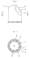
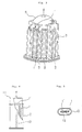
- Figures 1 to 3 are respectively a side view, a cross sectional view, and a perspective view of the outer periphery of the inner cylinder, showing one embodiment of the thermal decomposition furnace of the present invention;
- Figure 4 and Figure 5 are respectively a side view and a cross sectional view showing another embodiment of the thermal decomposition furnace of the invention;
- Figure 6 is a simulated view explaining the principle of the thermal decomposition furnace of the invention; and
- Figure 7 is a similar simulated view of a known system thermal decomposition furnace.
- According to one embodiment of the thermal decomposition furnace of the invention illustrated in Figures 1 to 3, an outer cylinder (4) and an inner cylinder (5) are provided with a cooling mechanism, and said inner cylinder (5) is provided in its outer periphery with a plurality of cylindrical, thermal decomposition chambers (6) each of which contains inverted U-shaped silicon filaments (1). A unit thermal decomposition chamber (6) has at its center a low shield (2) and the bridge portion (1') of said silicon filaments (1) is of such height that it can cross said low shield (2) but is not brought into contact therewith. The outer circumference of said thermal decomposition chamber (6) is made of a high shield (3) which is constructed to separate other thermal decomposition chamber units. Additionally, these high and low shields (3), (2) are provided with cooling mechanisms (not shown) respectively.
- According to another embodiment of the thermal decomposition furnace of the invention, which is illustrated in Figures 4 and 5, the furnace consists of a portion (10) for storing the inverted U-shaped silicon filaments and a disengageable cover (11), said storing portion (10) is provided at its center with a partition (12), each of the thermal decomposition chambers is of cylindrical shape, the height of said partition (12) extends not to contact its bridge portion (1') in the case of setting inverted U-shaped silicon rods (1) to the central axis of each thermal decomposition chamber. Additionally, the thermal decomposition furnaces can be arranged in plurality in which case they can be electrically connected (not shown), decomposition gas can be guided, and the charging can be done in parallel.
- Next, the experimental result of the present invention is described below.
- Eighteen silicon filaments (1), each having a diameter of 7 mm and a length of 2,000 mm, were set in a thermal decomposition furnace as shown in FIGS. 1 to 3, and the respective unit silicon filaments are connected with one another by respective bridges (1') while holding low shielding plates (2) therebetween thereby directly, electrically heating the silicon filaments. The respective silicon filaments are set in the center of a cylindrical zone enclosed by an outer cylinder (4) and an inner cylinder (5), and the bridge portion of a unit silicon filaments is isolated from neighboring unit silicon filaments through high shields (3). The speed of growth of each silicon rod by the thermal decomposition reaction was kept at 4 µm/min until the diameter of each rod reached 80 mm. This means that compared with the period of time during which four silicon filaments having a length of 1,200 mm were grown until the diameter of each reached 80 mm as above in a conventional thermal decomposition furnace i.e. the one as described in Patent Publication No. 56-45850, the period of time could be shortened by about 10% despite the increase in number and length of the pieces of silicon filaments.
- Six sets of the thermal decomposition furnace as shown in FIG. 2 were manufactured. Since the gas line system, the power source system, the control system and the like are carried out in one place the six sets of thermal decomposition furnace form substantially a single apparatus. The silicon filaments of the same size as in EXAMPLE 1 were set in these thermal decomposition furnaces to grow them at a speed of 4.5 µm/min until their diameters reached 90 mm, when mixing or incorporation of powdery silicon was not observed. It was confirmed that because of the symmetrical shape of the spaces around the silicon filaments it was possible to manufacture the silicon rods thicker and longer and in more quantity at a shorter period of time than in the conventional system.
- The functions and effects of the present invention are enumerated as follows.
- (1) The material of the bridges which are used in manufacturing the semi-conductive polycrystal silicon rods are either silicon rod or metallic rod having a high melting point, but since the bridges need to be insulated from the furnace walls they must be separated from the walls. Conventionally, the upper portions of the silicon filaments and the bridge portions were not shielded. However, now that thicker and longer silicon rods are demanded in a large quantity charging as described above, it is not possible to ignore the heat radiated from the bridge portions. To ensure a complete heat shielding, therefore, the structure of the present furnace is made to isolate the whole circumference of each bridge. Thus, compared with the manufacture according to the known structure it is now possible to manufacture thicker and longer and in larger quantity at a shorter period of time.
- (2) Further, by positioning single silicon filaments in the center of a cooled cylindrical shield the gas rises become symmetrical about the silicon filaments. Since the depositing rate of the silicon upon the silicon filaments is determined by the feeding speed of the monosilane to the material gas, the gaseous starting material is consumed in even quantity in any part so as to solve the irregularity of concentration if, as described above, the gas flow rate around the silicon filaments retains symmetry. The decomposition reaction in the gas phase mostly proceeds at the places of maximum concentration, so that conventionally the conditions of total thermal decomposition had to meet said portions of maximum concentration. However, since such requirements are no longer needed it is possible to aim at reducing the cost and improving the productivity to a greater extent.
- (3) Even according to the known structure of the thermal decomposition furnace it was capable of producing thicker silicon rods by decreasing the supplied amount of monosilane gas and lowering the monosilane concentration, but the productivity was too poor. Even such a case had a limitation, and the maximum diameter of the silicon rods which could be produced without mixing or incorporation of powdery silicon was at most 100 mm. According to the present invention, however, it suffices just to retard the growing speed a little even when producing a product having a 100 mm diameter.
- As described above in detail, the present invention meets such demands as improving the productivity, reducing the cost, and presenting products of thicker diameter and the products can be presented at a shorter period of time than in the conventional technique whereby many effects can be produced.
Claims (2)
- A method of manufacturing high-purity, semi-conductive, polycrystalline silicon rods by subjecting monosilane gas to thermal decomposition to deposit silicon on a plurality of silicon filaments (1) heated by electric current directly therethrough while shielding the heat between said silicon filaments and shielding radiant heat from the bridge portion (1') which electrically connects the individual heated silicon filaments characterized in that the individual inverted U-shaped silicon carrier members (1) are arranged across a cooled shield (2) on the central axis of each of pairs of individual cylindrical thermal decomposition chambers which are isolated by cooled shields (3) whereby the monosilane gas is decomposed at a uniform flow rate and concentration..
- A thermal decomposition furnace for manufacturing semi-conductive polycrystalline silicon rods said furnace having electrical connections, a guide portion for the gas to be decomposed, and a gas discharge portion, said thermal decomposition furnace comprising an outer cylinder (4) and an inner cylinder (5) each having a cooling structure, the outer periphery of said inner cylinder being provided with a plurality of thermal decomposition chambers (6) in which inverted U-shaped electrically heated silicon filaments (1) can be arranged, each individual thermal decomposition chamber being provided at its center with a low shield (2) the bridge portions (1') of said silicon filaments being capable of arrangement across the shield without contacting it, and said outer periphery of the thermal decomposition chamber comprising a high shield (3), both the low shield (2) and the high shield (3) being provided with a cooling mechanism.
Applications Claiming Priority (1)
| Application Number | Priority Date | Filing Date | Title |
|---|---|---|---|
| PCT/JP1990/000833 WO1992000245A1 (en) | 1990-06-27 | 1990-06-27 | Method of producing polycrystalline silicon rods for semiconductors and thermal decomposition furnace therefor |
Publications (3)
| Publication Number | Publication Date |
|---|---|
| EP0536394A1 EP0536394A1 (en) | 1993-04-14 |
| EP0536394A4 EP0536394A4 (en) | 1993-05-26 |
| EP0536394B1 true EP0536394B1 (en) | 1996-05-15 |
Family
ID=13986598
Family Applications (1)
| Application Number | Title | Priority Date | Filing Date |
|---|---|---|---|
| EP90909847A Expired - Lifetime EP0536394B1 (en) | 1990-06-27 | 1990-06-27 | Method of producing polycrystalline silicon rods for semiconductors and thermal decomposition furnace therefor |
Country Status (3)
| Country | Link |
|---|---|
| EP (1) | EP0536394B1 (en) |
| DE (1) | DE69027048T2 (en) |
| WO (1) | WO1992000245A1 (en) |
Cited By (2)
| Publication number | Priority date | Publication date | Assignee | Title |
|---|---|---|---|---|
| CN102923710A (en) * | 2012-11-19 | 2013-02-13 | 中国恩菲工程技术有限公司 | Polycrystalline silicon reducing furnace |
| US10208381B2 (en) | 2014-12-23 | 2019-02-19 | Rec Silicon Inc | Apparatus and method for managing a temperature profile using reflective energy in a thermal decomposition reactor |
Families Citing this family (8)
| Publication number | Priority date | Publication date | Assignee | Title |
|---|---|---|---|---|
| EP0671409A3 (en) * | 1994-03-11 | 1996-06-12 | Hoechst Ag | Malonic acid derivatives having anti-adhesive properties. |
| DE4408248A1 (en) * | 1994-03-11 | 1995-09-14 | Hoechst Ag | Physiologically acceptable and physiologically degradable carbohydrate mimetics, process for their preparation and their use |
| CN102190304B (en) * | 2010-03-08 | 2015-04-15 | 三菱综合材料株式会社 | Apparatus for producing trichlorosilane |
| CN102190305B (en) * | 2010-03-15 | 2014-10-29 | 三菱综合材料株式会社 | Apparatus for producing trichlorosilane |
| JP2013523596A (en) * | 2010-04-12 | 2013-06-17 | エムイーエムシー・エレクトロニック・マテリアルズ・ソシエタ・ペル・アチオニ | Bell jar for Siemens reactor including heat radiation shield |
| EP2423352A1 (en) * | 2010-08-24 | 2012-02-29 | Centesil S.L. | Thermal shield for silicon production reactors |
| DE102011084137A1 (en) | 2011-10-07 | 2013-04-11 | Wacker Chemie Ag | Apparatus and method for depositing polycrystalline silicon |
| US20220274838A1 (en) * | 2019-07-12 | 2022-09-01 | Tokuyama Corporation | Production method for polycrystalline silicon |
Family Cites Families (3)
| Publication number | Priority date | Publication date | Assignee | Title |
|---|---|---|---|---|
| JPS53106626A (en) * | 1977-03-02 | 1978-09-16 | Komatsu Mfg Co Ltd | Method of making high purity rod silicon and appratus therefor |
| JPS61101410A (en) * | 1984-10-24 | 1986-05-20 | Hiroshi Ishizuka | Production of polycrystalline silicon and apparatus therefor |
| US4805556A (en) * | 1988-01-15 | 1989-02-21 | Union Carbide Corporation | Reactor system and method for forming uniformly large-diameter polycrystalline rods by the pyrolysis of silane |
-
1990
- 1990-06-27 EP EP90909847A patent/EP0536394B1/en not_active Expired - Lifetime
- 1990-06-27 WO PCT/JP1990/000833 patent/WO1992000245A1/en not_active Ceased
- 1990-06-27 DE DE69027048T patent/DE69027048T2/en not_active Expired - Fee Related
Cited By (2)
| Publication number | Priority date | Publication date | Assignee | Title |
|---|---|---|---|---|
| CN102923710A (en) * | 2012-11-19 | 2013-02-13 | 中国恩菲工程技术有限公司 | Polycrystalline silicon reducing furnace |
| US10208381B2 (en) | 2014-12-23 | 2019-02-19 | Rec Silicon Inc | Apparatus and method for managing a temperature profile using reflective energy in a thermal decomposition reactor |
Also Published As
| Publication number | Publication date |
|---|---|
| DE69027048D1 (en) | 1996-06-20 |
| EP0536394A1 (en) | 1993-04-14 |
| EP0536394A4 (en) | 1993-05-26 |
| DE69027048T2 (en) | 1997-01-02 |
| WO1992000245A1 (en) | 1992-01-09 |
Similar Documents
| Publication | Publication Date | Title |
|---|---|---|
| EP0324504B1 (en) | Method for forming uniformly large-diameter polycrystalline rods by the pyrolysis of silane and a reactor system therefor | |
| CN1020481C (en) | Manufacturing equipment for single silicon crystal | |
| US5478396A (en) | Production of high-purity polycrystalline silicon rod for semiconductor applications | |
| US4150168A (en) | Method and apparatus for manufacturing high-purity silicon rods | |
| US6365225B1 (en) | Cold wall reactor and method for chemical vapor deposition of bulk polysilicon | |
| US5080873A (en) | Apparatus for growing crystals | |
| EP0536394A1 (en) | Method of producing polycrystalline silicon rods for semiconductors and thermal decomposition furnace therefor | |
| WO2013007108A1 (en) | Method for growing thin-plate silicon crystal | |
| US5367981A (en) | Apparatus for manufacturing crystals through floating zone method | |
| US5382419A (en) | Production of high-purity polycrystalline silicon rod for semiconductor applications | |
| WO1991017952A1 (en) | Process for producing crystalline silicon ingot in a fluidized bed reactor | |
| JP7611193B2 (en) | Polycrystalline silicon rod, polycrystalline silicon rod and method for producing same | |
| Dietze et al. | Float-zone grown silicon | |
| JPH06172093A (en) | Semiconductor grade polycrystalline silicon manufacturing reactor | |
| JP2006069888A (en) | Manufacturing method and manufacturing apparatus for polycrystalline silicon rod | |
| US4590024A (en) | Silicon deposition process | |
| JP5642755B2 (en) | Apparatus and method for depositing polycrystalline silicon | |
| JP7824935B2 (en) | Crystal pulling system having a cover member for covering a silicon charge and method for growing a silicon melt in a crucible assembly - Patents.com | |
| JP2769388B2 (en) | Method for producing polycrystalline silicon rod for semiconductor and thermal decomposition furnace thereof | |
| CN113564695B (en) | Seed crystal laying method for casting monocrystalline silicon, monocrystalline silicon ingot and casting method thereof | |
| JPH07109198A (en) | Device and method for producing bar-like high-purity silicon for semiconductor | |
| JPWO1992000245A1 (en) | Manufacturing method of polycrystalline silicon rods for semiconductors and pyrolysis furnace | |
| JPH07110798B2 (en) | Single crystal manufacturing equipment | |
| JPH05117074A (en) | Method for producing semiconductor single crystal and apparatus therefor | |
| JPH04187585A (en) | Device of growing crystal |
Legal Events
| Date | Code | Title | Description |
|---|---|---|---|
| PUAI | Public reference made under article 153(3) epc to a published international application that has entered the european phase |
Free format text: ORIGINAL CODE: 0009012 |
|
| 17P | Request for examination filed |
Effective date: 19930121 |
|
| AK | Designated contracting states |
Kind code of ref document: A1 Designated state(s): DE FR |
|
| A4 | Supplementary search report drawn up and despatched |
Effective date: 19930406 |
|
| AK | Designated contracting states |
Kind code of ref document: A4 Designated state(s): DE FR |
|
| 17Q | First examination report despatched |
Effective date: 19941024 |
|
| GRAH | Despatch of communication of intention to grant a patent |
Free format text: ORIGINAL CODE: EPIDOS IGRA |
|
| GRAA | (expected) grant |
Free format text: ORIGINAL CODE: 0009210 |
|
| AK | Designated contracting states |
Kind code of ref document: B1 Designated state(s): DE FR |
|
| REF | Corresponds to: |
Ref document number: 69027048 Country of ref document: DE Date of ref document: 19960620 |
|
| ET | Fr: translation filed | ||
| PLBE | No opposition filed within time limit |
Free format text: ORIGINAL CODE: 0009261 |
|
| STAA | Information on the status of an ep patent application or granted ep patent |
Free format text: STATUS: NO OPPOSITION FILED WITHIN TIME LIMIT |
|
| 26N | No opposition filed | ||
| PGFP | Annual fee paid to national office [announced via postgrant information from national office to epo] |
Ref country code: FR Payment date: 20000612 Year of fee payment: 11 |
|
| PGFP | Annual fee paid to national office [announced via postgrant information from national office to epo] |
Ref country code: DE Payment date: 20000626 Year of fee payment: 11 |
|
| PG25 | Lapsed in a contracting state [announced via postgrant information from national office to epo] |
Ref country code: FR Free format text: LAPSE BECAUSE OF NON-PAYMENT OF DUE FEES Effective date: 20020228 |
|
| PG25 | Lapsed in a contracting state [announced via postgrant information from national office to epo] |
Ref country code: DE Free format text: LAPSE BECAUSE OF NON-PAYMENT OF DUE FEES Effective date: 20020403 |