EP0534768A1 - Uncooled infrared detector and method for forming the same - Google Patents
Uncooled infrared detector and method for forming the same Download PDFInfo
- Publication number
- EP0534768A1 EP0534768A1 EP92308737A EP92308737A EP0534768A1 EP 0534768 A1 EP0534768 A1 EP 0534768A1 EP 92308737 A EP92308737 A EP 92308737A EP 92308737 A EP92308737 A EP 92308737A EP 0534768 A1 EP0534768 A1 EP 0534768A1
- Authority
- EP
- European Patent Office
- Prior art keywords
- layer
- variable resistor
- bolometer
- forming
- spectral range
- Prior art date
- Legal status (The legal status is an assumption and is not a legal conclusion. Google has not performed a legal analysis and makes no representation as to the accuracy of the status listed.)
- Granted
Links
Images



Classifications
-
- G—PHYSICS
- G01—MEASURING; TESTING
- G01J—MEASUREMENT OF INTENSITY, VELOCITY, SPECTRAL CONTENT, POLARISATION, PHASE OR PULSE CHARACTERISTICS OF INFRARED, VISIBLE OR ULTRAVIOLET LIGHT; COLORIMETRY; RADIATION PYROMETRY
- G01J5/00—Radiation pyrometry, e.g. infrared or optical thermometry
- G01J5/10—Radiation pyrometry, e.g. infrared or optical thermometry using electric radiation detectors
- G01J5/20—Radiation pyrometry, e.g. infrared or optical thermometry using electric radiation detectors using resistors, thermistors or semiconductors sensitive to radiation, e.g. photoconductive devices
-
- H—ELECTRICITY
- H04—ELECTRIC COMMUNICATION TECHNIQUE
- H04N—PICTORIAL COMMUNICATION, e.g. TELEVISION
- H04N25/00—Circuitry of solid-state image sensors [SSIS]; Control thereof
- H04N25/60—Noise processing, e.g. detecting, correcting, reducing or removing noise
- H04N25/67—Noise processing, e.g. detecting, correcting, reducing or removing noise applied to fixed-pattern noise, e.g. non-uniformity of response
- H04N25/671—Noise processing, e.g. detecting, correcting, reducing or removing noise applied to fixed-pattern noise, e.g. non-uniformity of response for non-uniformity detection or correction
-
- H—ELECTRICITY
- H04—ELECTRIC COMMUNICATION TECHNIQUE
- H04N—PICTORIAL COMMUNICATION, e.g. TELEVISION
- H04N25/00—Circuitry of solid-state image sensors [SSIS]; Control thereof
- H04N25/60—Noise processing, e.g. detecting, correcting, reducing or removing noise
- H04N25/67—Noise processing, e.g. detecting, correcting, reducing or removing noise applied to fixed-pattern noise, e.g. non-uniformity of response
- H04N25/671—Noise processing, e.g. detecting, correcting, reducing or removing noise applied to fixed-pattern noise, e.g. non-uniformity of response for non-uniformity detection or correction
- H04N25/673—Noise processing, e.g. detecting, correcting, reducing or removing noise applied to fixed-pattern noise, e.g. non-uniformity of response for non-uniformity detection or correction by using reference sources
- H04N25/674—Noise processing, e.g. detecting, correcting, reducing or removing noise applied to fixed-pattern noise, e.g. non-uniformity of response for non-uniformity detection or correction by using reference sources based on the scene itself, e.g. defocusing
-
- H—ELECTRICITY
- H04—ELECTRIC COMMUNICATION TECHNIQUE
- H04N—PICTORIAL COMMUNICATION, e.g. TELEVISION
- H04N25/00—Circuitry of solid-state image sensors [SSIS]; Control thereof
- H04N25/70—SSIS architectures; Circuits associated therewith
- H04N25/76—Addressed sensors, e.g. MOS or CMOS sensors
-
- H—ELECTRICITY
- H10—SEMICONDUCTOR DEVICES; ELECTRIC SOLID-STATE DEVICES NOT OTHERWISE PROVIDED FOR
- H10F—INORGANIC SEMICONDUCTOR DEVICES SENSITIVE TO INFRARED RADIATION, LIGHT, ELECTROMAGNETIC RADIATION OF SHORTER WAVELENGTH OR CORPUSCULAR RADIATION
- H10F39/00—Integrated devices, or assemblies of multiple devices, comprising at least one element covered by group H10F30/00, e.g. radiation detectors comprising photodiode arrays
- H10F39/10—Integrated devices
- H10F39/12—Image sensors
- H10F39/191—Photoconductor image sensors
- H10F39/193—Infrared image sensors
- H10F39/1935—Infrared image sensors of the hybrid type
Definitions
- This invention generally relates to the fabrication of semiconductor devices and specifically to an uncooled infrared detector and a method for forming the same.
- Infrared detectors may be classified in various ways, such as scanning or staring arrays, cryogenic (typically liquid nitrogen temperatures) or uncooled detectors, 3-5 micron or 8-12 micron spectral sensitivity range, and photon or thermal detection mechanism.
- Cryogenic infrared detectors are typically made of small bandgap (about 0.1-0.2 eV) semiconductors such as HgCdTe and operate as photo-diodes or photocapacitors by photon absorption to produce electron-hole pairs.
- small bandgap about 0.1-0.2 eV
- HgCdTe small bandgap semiconductors
- HgCdTe small bandgap semiconductors
- photo-diodes or photocapacitors by photon absorption to produce electron-hole pairs.
- uncooled infrared detectors cannot make use of small bandgap semiconductors because the bandgap is only about 4kT at room temperature and dark current swamps any signal. Consequently, uncooled infrared detectors rely on the other physical phenomena and are less sensitive than cryogenic detectors but do not require cooling apparatus or its energy consumption. For portable, low power applications where the greater detectivity of cryogenic detectors is not needed, the preferred choice is an uncooled thermal detector: infrared photons are absorbed and the resultant heating of the absorbing element is detected.
- the thermal detector is usually one of three types: (1) pyroelectric detector, (2) thermocouple, or (3) bolometer.
- the pyroelectric detector uses a ferroelectric ceramic material (such as BaSrTiO3) at operating temperatures (typically 0 °C to 150 °C) a little below its Curie temperature.
- the preferred ferroelectric materials have a large change in spontaneous dielectric polarization at operating temperatures, and the heating of the ferroelectric is detected by sensing the induced voltage created by the generation of charge across a capacitor with the ferroelectric as insulator.
- a ferroelectric ceramic material such as BaSrTiO3
- the pyroelectric detector is a hybrid approach that has problems when extended to large detector arrays (such as arrays of 256 by 256 pixels) due to ferroelectric material defects, contact defects, and bump bonding defects which imply low yields.
- Thermocouples rely on the change in contact potential of a junction of dissimilar conductors with temperature; see for example G. Lahiji et al, A Monolithic Thermopile Detector Fabricated Using Integrated-Circuit Technology, 1980 IEEE IEDM Tech.Dig. 676 which uses bismuthantimony or polysilicon-gold couples in monolithic arrays on silicon.
- Bolometers typically rely on the temperature change of resistance of thermally isolated thin metal films or semiconductor films.
- the thin films may be fabricated on a suspended dielectric film in a silicon substrate and may be located adjacent to monolithic detection circuitry on the silicon substrate.
- the dielectric film is thermally isolated from the remainder of the silicon substrate by etching away the silicon from beneath the dielectric film so that it is suspended. See for example K. C. Liddiard, 24 Infrared Physics 57 (1984) and 26 Infrared Physics 43 (1986) which includes amorphous silicon films for resistance change with temperature plus abutting nickel films for infrared absorption and electrical contact.
- K. C. Liddiard 24 Infrared Physics 57 (1984) and 26 Infrared Physics 43 (1986) which includes amorphous silicon films for resistance change with temperature plus abutting nickel films for infrared absorption and electrical contact.
- thermocouples and bolometers avoid the yield problem of the pyroelectric detectors because they can be monolithically fabricated on a silicon wafer along with the detection circuitry.
- thermocouples and bolometers have the problem of lower detectivities than pyroelectric detectors.
- a bolometer for detecting radiation in a spectral range includes an integrated circuit substrate and a pixel body spaced from the substrate by at least one pillar.
- the pixel body comprises an absorber material, such as titanium for example, for absorbing radiation over a broad range including the spectral range, 7 to 12 microns for example.
- the absorber material heats the pixel body to a temperature which is proportional to the absorbed radiation.
- An insulating material is formed over the absorber material.
- a variable resistor material possible amorphous silicon for example, with an electrical resistance corresponding to the temperature of the pixel body is formed over said insulating layer. A current flows through the variable resistor material substantially parallel to the integrated circuit substrate for detection.
- a method of forming a bolometer cell includes the steps of forming a temporary layer on a substrate.
- a layer of absorber material is formed on the temporary layer and patterned and etched.
- An insulating layer is formed over the layer of absorber material and patterned and etched.
- a layer of variable resistor material is then formed over the insulating layer.
- At least one pillar hole is formed in the layer of variable resistor material and the underlying portion of the temporary layer.
- a conducting pillar is formed in each of the pillar holes.
- the variable resistor material is patterned and etched to form a temperature variable resistor. At least two contacts are formed from the pillars to the temperature variable resistor. Finally, the temporary layer is removed.
- An advantage of the invention is that it provides a producible infrared detection cell which may be fabricated at reasonable costs relative to other presently available systems.
- the cell of this invention may be operated at temperatures near room temperature and therefore there is no requirement for cryogenic equipment. As a result, the cost and size limitations normally associated with cryogenic systems are avoided.
- the current path through the temperature sensitive resistor is parallel to the substrate, as opposed to vertically through the resistor, there is a relatively long conductive path. Because of this, a more reasonable voltage coefficient of resistance may be achieved and accordingly a more linear device may be built.
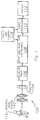
- Figure 1 illustrates in schematic diagram view an infrared imagery system, generally noted 100, which includes infrared lens system 102, optional mechanical chopper 104 (this element is not necessary for the present invention), bolometer array 106, drive and readout electronics 108 for array 106, video processor 110, display 112, and timing and control electronics 114.
- the lens system 102 images infrared radiation emitted by warm object 116 onto array 106.
- Chopper 104 may be a rotating disk with openings that periodically block and let pass the infrared radiation collected by lens system 102.
- the chopper 104 is of the focusing/defocusing type.
- array 106 includes 65,536 bolometers arranged in 256 rows by 256 columns; each bolometer corresponds to a pixel in the image of the warm body 116 plus surrounding scene in the field of view of the lens system 102.
- Array 106 may be housed in a stainless vacuum chamber with an infrared transparent window formed in one side or surrounded by an atmosphere of gate with low thermal transport. The window is positioned so that radiation from the scene with warm body 116 passes through the window onto array 106.
- the design considerations for a microbolometer image sensor can be identified by considering each element in the chain of events which lead to the conversion of the IR flux to electrical signal.
- the first step is to convert the IR flux to heat energy stored in the detector pixel. If this process is to be as large as possible, the absorption efficiency of the pixel should be 100% over the IR band of interest. In order for the temperature rise of the pixel element to be large, the heat capacity of the pixel must be minimized and the thermal isolation of the pixel from the surrounding structure must be maximized. To maximize the signal output for a given temperature change of the pixel, the coefficient of resistance with temperature of the bolometer resistor should be large as possible.
- the pixel resistance value must be such as to be compatible with the readout electronics and to control the power dissipation in the pixel at the readout conditions required by the readout electronics.
- the electrical noise generated by both the pixel resistance and the readout pre amplifier must be sufficiently small to provide the necessary imaging performance.
- Figure 2 illustrates a first preferred embodiment cross section of a structure which results in an acceptable engineering trade-off between the conflicting requirements.
- the pixel body 120 is spaced above a silicon substrate 122, which contains the pixel preamplifier (not shown) associated with the particular pixel, by pillars 124.
- the pillars 124 may be made of aluminum or other materials which meet the structural and conductive requirements such as other metals. These pillars 124 control the separation between the pixel 120 and the substrate mirror 126 formed by an infrared reflective film deposited on the substrate 122.
- the reflective film may be aluminum or other appropriate metals.
- the mirror 126 serves to reflect the IR radiation which is not absorbed on the first path through the pixel back into the pixel for additional absorption.
- the pixel body 120 may ideally be spaced ⁇ /4 microns ( ⁇ is the wavelength of IR radiation being detected - typically between 7 and 12 microns) above the mirror 126 to gain resonant performance. In more practical cases, however, the spacing is determined by processing or other concerns. Experimentation has shown that IR absorbtion of this structure is not strongly dependent on the mirror to absorber spacing about ⁇ /4 so the spacing is usually selected to facilitate fabrication.
- the mirror 126 may also serve as one of the pixel interconnects between the integrated circuit (IC) and the pixel resistor.
- a conductive pad 128 serves as the other interconnect between the pixel and the IC. If the mirror 126 is not one of the pixel interconnects, an additional pad (not shown) may be used. It should be noted that if the first pass IR absorbtion efficiency is high enough, the mirror 126 may be omitted.
- the pixel body 120 is composed of sequential layers of films which perform various functions needed for detection.
- the first film layer 130 is a passivation layer which protects the primary absorber layer 132 from damage during the fabrication process. Any film with the required chemical properties can be used. Exemplary films include silicon dioxide, amorphous silicon and silicon nitride.
- the next layer, the absorber layer 132 is a thin conductive layer which uses free electron absorption to convert the incident IR to heat in the pixel. This absorber layer is typically a metal such as titanium, nickel or chromium.
- an insulating layer 134 is formed to isolate the absorber layer 132, a conductor, from the next layer, the temperature sensitive resistive film 136 of the detector.
- This insulating film 134 may also serve as a secondary absorber of the IR radiation.
- Any insulating film may be used for insulating layer 134, for example silicon dioxide, silicon nitride or amorphous silicon.
- the layer 134 may be the same material as passivation layer 130.
- the final film is the temperature sensitive resistive layer 136 which forms the bolometer resistor and may serve as a secondary IR absorber.
- the bolometer resistor material 136 may be amorphus silicon doped to 7 x 10 ⁇ 4/ ⁇ -cm.
- any semiconductor or semimetal with an appropriate TCR (temperature coefficient of resistance) can be used.
- An ideal bolometer has four characteristics, namely 1) large temperature dependence, 2) 100% IR absorption, 3) minimal thermal mass, and 4) high thermal isolation. Therefore, the materials chosen to form the device are chosen to optimize these characteristics. For example, the absorption layer 132 is chosen such that the maximum amount of IR energy is converted to heat. In practical cases, with materials such as titanium, 80 to 90% absorption has been achieved.
- variable resistor is formed of an appropriate semiconductor
- the spectral range can include visible light.
- the visible light is absorbed by the semiconductor resulting in carrier generation in the bolometer resistor. This changes the detector resistance.
- the temperature sensitive resistance material 136 must change resistance such that the heat, and therefore the IR radiation, can be detected in the circuit below.
- the electrical noise generated in the resistor must be minimized.
- noise is 1/F noise.
- 1/F noise is typically generated by carrier trapping in film defects.
- Preparation of low noise films is currently an empirical art. Therefore, materials which maximize thermal resistance dependence but minimize electrical noise are chosen. Some examples are amorphous silicon, germanium, and metal oxides. But other materials which meet these criteria may also be used.
- the third characteristic, minimal thermal mass, is optimized by choosing films with appropriate physical strength so that each of the films may be made very thin.
- the fourth characteristic, high thermal isolation is optimized by thermally isolating the pixel from the remainder of the cell. This goal is accomplished by spacing the pixel body 120 from the substrate 122. Other thermal isolation strategies will be discussed below with reference to Figure 3.
- the temperature sensitive resistor 120 is connected to the pillar 124, which is in turn connected to the IC formed in the substrate 122, through interconnects 138.
- the interconnects 138 may be formed by any suitable conductive material.
- FIG 3 shows the plan view of the pixel structure.
- the central portion of the pixel 120 provides both the absorption of IR radiation and the body of the pixel resistor.
- the support arms 142 along two edges of the pixel provide long, thin, narrow thermal isolation resistors between the resistor body 120 and the underlying spacer pillars 124 located at the substrate ends of these thermal resistors 142.
- the support arms are spaced from the resistor body by air gaps 146. In this way, the pixel body 140 is thermally isolated from the substrate 122.
- gaps 146 (which may be air gaps) separate the support arms 142 from the pixel body 120 on three of the four sides.
- the gaps 146 can be extended along the remaining two sides of the pixel body if additional thermal isolation is desired.
- the mechanical strength of the support arms 142 will be substantially weakened by this change. For each individual design, this trade-off must be considered.
- a very thin film of a conductive material may be applied to provide electrical contacts to the resistor body 120 located in the center of the pixel. This film is as thin as possible in order to avoid compromising the thermal isolation of the pixel.
- the metal tabs 144 shown in Figure 3 provide mechanical support and electrical contacts between the ends of the support arms 142 and the tops of the spacer pillars 124.
- the contact regions shown are an artifact of the fabrication process and do not make a direct contribution to the structure.
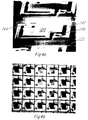
- FIG. 4a A SEM (secondary electron microscope) photomicrograph of a completed pixel is illustrated in Figure 4a.
- Figure 4b shows an array of mechanical pixels to demonstrate the fabrication process on closely packed arrays.
- the current execution of these pixel designs uses an absorber passivation layer 130 of SiO2 (silicon dioxide) deposited by plasma CVD (chemical vapor deposition) with a thickness of about 250 ⁇ .
- the absorber layer 132 is composed of 140 ⁇ of Ti (titanium) deposited over the passivation layer 130.
- the insulator layer 134 is also formed of a plasma deposition SiO2 with a thickness varying between 1000 and 2000 ⁇ .
- the resistive layer 136 is composed of a-Si (amorphous silicon) deposited by plasma CVD and doped for electrical conduction with phosphorous derived from PF5 (phosphorous pentafluoride) feed stock.
- the temperature coefficient of resistance of this film as presently deposited is 3 to 3.5% and the conductivity is approximately 8 x 10 ⁇ 4 cm ⁇ 1 ⁇ 1.
- the selection of these films for the pixel structure is partly based on process convenience and partly based on critical electrical and mechanical considerations.
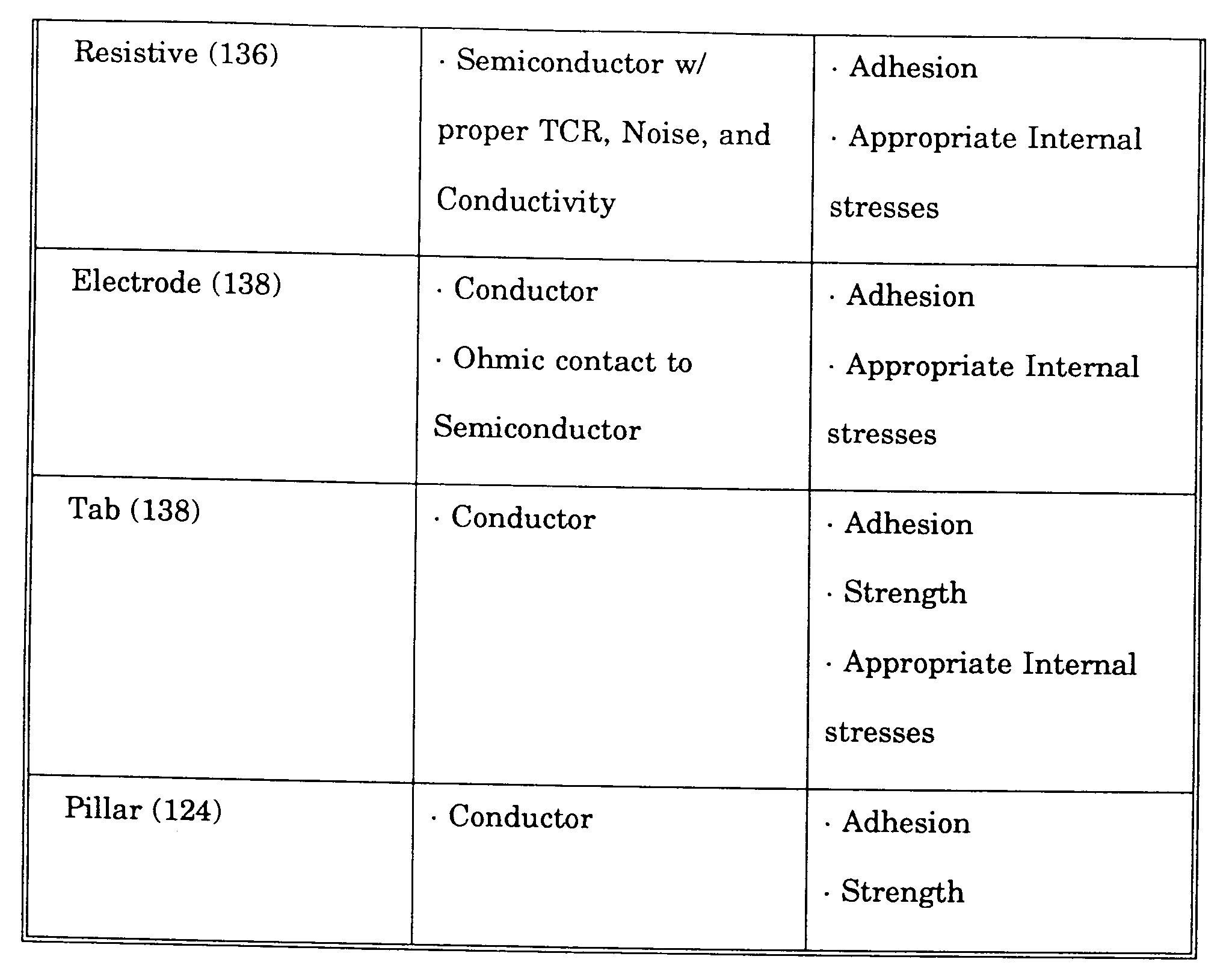
- the insulator film could be silicon nitride, zinc sulfide, or amorphous silicon, rather than silicon dioxide. Table 1 summarizes some of the more important of these electrical and mechanical properties.
- Infrared radiation impinges upon the top surface of the pixel body 120 and is absorbed in the absorbing layer 132 causing the pixel temperature to rise.
- the resistance of the temperature sensitive resistive layer 136 then changes in correspondence with the temperature change, i.e., in correspondence with the change in intensity of the IR radiation. This change in resistance can be monitored by the integrated circuitry formed in the substrate 122.
- the current flows from interconnect 138a through resistive layer 136 in parallel with the substrate 122 and down through interconnect 138b. Since the current flows laterally across the pixel, as opposed by vertically into and then out of the pixel, the conduction path is considerably longer than some prior art applications. This difference, possibly from 3000 ⁇ to 30 ⁇ (2 orders of magnitude), gives a considerable improvement in the voltage coefficient of resistance and therefore gives a very linear resistor.
- Figs. 5-10 The major process steps of a current fabrication process embodiment are illustrated in the cross-sectional views of Figs. 5-10.
- a film of aluminum is deposited and patterned to reveal the electrical contacts 126 and 128 to the circuit.
- a film 150 of polyimide (organic polymer) is deposited to a thickness of 2 ⁇ m by conventional spin coating often used for this material.
- the film 150 is subsequently baked to insure stability at elevated temperatures.
- the absorber passivation film (currently SiO2) is applied by plasma CVD, typically a substrate temperature of 175°C.
- the Ti absorber film 132 is deposited by DC magnitron sputtering.
- the Ti film 132 is patterned in the shape of the body of the pixel resistor, without the support arms, by plasma etching in a mixture of BCl3 (boron trichloride) and other gases as illustrated in Figure 7.
- the insulator film 134 of SiO2 is now applied using plasma CVD to a thickness between 1000 and 2000 ⁇ thick.
- This film and the underlying passivation film, now referred to as layer 135 in Figures 7-10, are patterned and plasma etched at one time using CF4 (carbon tetrafluoride) and O2 (oxygen) or other known SiO2 etchants.
- This pattern includes both the central body of the pixel and the support arms.
- a-Si (amorphous silicon) film 136 is deposited by plasma CVD using SiH4 (silane) and PF5 (phosphorous pentafluoride (boron fluoride may also be used) as feedstocks. The parameters of this deposition are chosen to provide the electrical and physical characteristics desired.
- the a-Si film 136 is selectively removed where needed to expose the underlying polyimide film 150 at the pillar locations. The polyimide is then removed down to the underlying metal contacts 126 or 128 of the IC formed in the substrate 122 using a plasma of oxygen and argon.
- the patterned a-Si film 136 is used as an etch mask during this etch step.
- the temperature sensitive a-Si film 136 is again patterned, this time in the outline of both the pixel body and the support arms by using photoresist processing and plasma etching in carbon tetrafluoride and oxygen.
- the structure is now re-coated with photoresist (not shown) in the negative of the pillar pattern and the aluminum pillars 124 are deposited by vacuum metalization to the 2.0 micron thickness of the polyimide film.
- the excess metal is then stripped from the structure using a specially developed lift-off process leaving the pillars 124 nested in holes in the polyimide film 150 and contacting the IC.
- the electrical boundary of the resistor body is now defined by a thin (100 ⁇ or less) film of a conductor deposited and patterned as shown in Figure 3. This film serves to provide low resistance contacts to the resistor body in the center of the pixel.
- the tab metalization is now applied by using two layers of photoresist.
- the first layer 152 is to fill the void between the polyimide 150 edges and the body of the pillars 124 and the second layer 154 is to define the tab pattern proper.
- the tab metal 138 is deposited over these photoresist films and the excess metal is removed by conventional lift-off processes. This completes the structure as shown in Figure 2 except for removing the underlying polyimide film 150.
- the substrate wafer may be sawed into individual arrays and the wafers cleaned by the usual chemical means before the polyimide film is removed from under the pixel. With the sawing and post saw cleanup complete, the underlying polyimide film is etched from under the pixel using a plasma of oxygen and argon. Typical etch times are currently about 3 to 5 hours using a substrate temperature of 150°C.
- the parameters of the structure just described may be further optimized. Further, the arrangement of the films in the structure may well be revised in order to simplify the fabrication procedure or to improve performance. For example, inverting this structure will allow the pixel body to be defined by a single patterning step and insure registration of the insulator and resistor films.
Landscapes
- Engineering & Computer Science (AREA)
- Multimedia (AREA)
- Signal Processing (AREA)
- Physics & Mathematics (AREA)
- General Physics & Mathematics (AREA)
- Spectroscopy & Molecular Physics (AREA)
- Transforming Light Signals Into Electric Signals (AREA)
- Photometry And Measurement Of Optical Pulse Characteristics (AREA)
- Radiation Pyrometers (AREA)
Abstract
Description
- This invention generally relates to the fabrication of semiconductor devices and specifically to an uncooled infrared detector and a method for forming the same.
- Detection of infrared radiation emitted by warm bodies provides an important method for night vision (perception without visible light). Infrared detectors may be classified in various ways, such as scanning or staring arrays, cryogenic (typically liquid nitrogen temperatures) or uncooled detectors, 3-5 micron or 8-12 micron spectral sensitivity range, and photon or thermal detection mechanism. Cryogenic infrared detectors are typically made of small bandgap (about 0.1-0.2 eV) semiconductors such as HgCdTe and operate as photo-diodes or photocapacitors by photon absorption to produce electron-hole pairs. For example, see U.S. Pat. No. 4,686,373 (Tew et al) which describes a hybrid system with HgCdTe photocapacitors glued to silicon signal processing circuitry.
- Uncooled infrared detectors cannot make use of small bandgap semiconductors because the bandgap is only about 4kT at room temperature and dark current swamps any signal. Consequently, uncooled infrared detectors rely on the other physical phenomena and are less sensitive than cryogenic detectors but do not require cooling apparatus or its energy consumption. For portable, low power applications where the greater detectivity of cryogenic detectors is not needed, the preferred choice is an uncooled thermal detector: infrared photons are absorbed and the resultant heating of the absorbing element is detected. The thermal detector is usually one of three types: (1) pyroelectric detector, (2) thermocouple, or (3) bolometer.
- The pyroelectric detector uses a ferroelectric ceramic material (such as BaSrTiO₃) at operating temperatures (typically 0 °C to 150 °C) a little below its Curie temperature. The preferred ferroelectric materials have a large change in spontaneous dielectric polarization at operating temperatures, and the heating of the ferroelectric is detected by sensing the induced voltage created by the generation of charge across a capacitor with the ferroelectric as insulator. For example, see U.S. Pat. Nos. 4,348,611 (Ruppel et al), 4,142,207 (McCormack et al), and 4,379,232 (Hopper).
- The pyroelectric detector is a hybrid approach that has problems when extended to large detector arrays (such as arrays of 256 by 256 pixels) due to ferroelectric material defects, contact defects, and bump bonding defects which imply low yields.
- Thermocouples rely on the change in contact potential of a junction of dissimilar conductors with temperature; see for example G. Lahiji et al, A Monolithic Thermopile Detector Fabricated Using Integrated-Circuit Technology, 1980 IEEE IEDM Tech.Dig. 676 which uses bismuthantimony or polysilicon-gold couples in monolithic arrays on silicon.
- Bolometers typically rely on the temperature change of resistance of thermally isolated thin metal films or semiconductor films. The thin films may be fabricated on a suspended dielectric film in a silicon substrate and may be located adjacent to monolithic detection circuitry on the silicon substrate. The dielectric film is thermally isolated from the remainder of the silicon substrate by etching away the silicon from beneath the dielectric film so that it is suspended. See for example K. C. Liddiard, 24 Infrared Physics 57 (1984) and 26 Infrared Physics 43 (1986) which includes amorphous silicon films for resistance change with temperature plus abutting nickel films for infrared absorption and electrical contact. The foregoing references are hereby incorporated by reference.
- Thermocouples and bolometers avoid the yield problem of the pyroelectric detectors because they can be monolithically fabricated on a silicon wafer along with the detection circuitry. However, thermocouples and bolometers have the problem of lower detectivities than pyroelectric detectors.
- Another bolometer approach is described in U.S. Patent No. 5,021,663 (Hornbeck). In this approach, current flows vertically through the detector with a relatively short resistance path which results in non-linear electrical characteristics and a larger voltage coefficient of resistance. Non-linear resistors compromise the performance of a detector array. Therefore, a cell with a large conduction path is desirable.
- Accordingly, improvements which overcome any or all of the problems are presently desirable.
- Other objects and advantages will be obvious, and will in part appear hereinafter and will be accomplished by the present invention which provides a method and apparatus for an uncooled infrared detector.
- A bolometer for detecting radiation in a spectral range is described herein. The bolometer includes an integrated circuit substrate and a pixel body spaced from the substrate by at least one pillar. The pixel body comprises an absorber material, such as titanium for example, for absorbing radiation over a broad range including the spectral range, 7 to 12 microns for example. The absorber material heats the pixel body to a temperature which is proportional to the absorbed radiation. An insulating material is formed over the absorber material. In addition, a variable resistor material, possible amorphous silicon for example, with an electrical resistance corresponding to the temperature of the pixel body is formed over said insulating layer. A current flows through the variable resistor material substantially parallel to the integrated circuit substrate for detection.
- A method of forming a bolometer cell includes the steps of forming a temporary layer on a substrate. A layer of absorber material is formed on the temporary layer and patterned and etched. An insulating layer is formed over the layer of absorber material and patterned and etched. A layer of variable resistor material is then formed over the insulating layer. At least one pillar hole is formed in the layer of variable resistor material and the underlying portion of the temporary layer. A conducting pillar is formed in each of the pillar holes. The variable resistor material is patterned and etched to form a temperature variable resistor. At least two contacts are formed from the pillars to the temperature variable resistor. Finally, the temporary layer is removed.
- An advantage of the invention is that it provides a producible infrared detection cell which may be fabricated at reasonable costs relative to other presently available systems.
- In addition, the cell of this invention may be operated at temperatures near room temperature and therefore there is no requirement for cryogenic equipment. As a result, the cost and size limitations normally associated with cryogenic systems are avoided.
- Further, since the current path through the temperature sensitive resistor is parallel to the substrate, as opposed to vertically through the resistor, there is a relatively long conductive path. Because of this, a more reasonable voltage coefficient of resistance may be achieved and accordingly a more linear device may be built.
- The above features of the present invention will be more clearly understood from consideration of the following descriptions in connection with accompanying drawings in which:
- Figure 1 shows a block diagram of an infrared detector system which includes a first preferred embodiment bolometer array;
- Figure 2 shows a cross-sectional view of a preferred embodiment bolometer cell;
- Figure 3 shows a top-view of a preferred embodiment bolometer cell;
- Figures 4a-4b are microphotographs of a infrared detector; and
- Figures 5-10 are cross-sectional views to aid in the understanding of an exemplary fabrication process.
- Corresponding numerals and symbols in the different figures refer to corresponding parts unless otherwise indicated.
- Reference is made to United States Patent Application No. 07/766,879, from which the present application claims priority, and to the corresponding European Patent Application No. (TI-15367) of even date with the present Application.
- The making and use of the presently preferred embodiments are discussed below in detail. However, it should be appreciated that the present invention provides many applicable inventive concepts which can be embodied in a wide variety of specific contexts. The specific embodiments discussed are merely illustrative of specific ways to make and use the invention, and do not delimit the scope of the invention.
- Figure 1 illustrates in schematic diagram view an infrared imagery system, generally noted 100, which includes infrared lens system 102, optional mechanical chopper 104 (this element is not necessary for the present invention),
bolometer array 106, drive andreadout electronics 108 forarray 106,video processor 110,display 112, and timing and control electronics 114. The lens system 102 images infrared radiation emitted by warm object 116 ontoarray 106.Chopper 104 may be a rotating disk with openings that periodically block and let pass the infrared radiation collected by lens system 102. In the preferred embodiment, thechopper 104 is of the focusing/defocusing type. In one embodiment,array 106 includes 65,536 bolometers arranged in 256 rows by 256 columns; each bolometer corresponds to a pixel in the image of the warm body 116 plus surrounding scene in the field of view of the lens system 102.Array 106 may be housed in a stainless vacuum chamber with an infrared transparent window formed in one side or surrounded by an atmosphere of gate with low thermal transport. The window is positioned so that radiation from the scene with warm body 116 passes through the window ontoarray 106. - The design considerations for a microbolometer image sensor can be identified by considering each element in the chain of events which lead to the conversion of the IR flux to electrical signal. The first step is to convert the IR flux to heat energy stored in the detector pixel. If this process is to be as large as possible, the absorption efficiency of the pixel should be 100% over the IR band of interest. In order for the temperature rise of the pixel element to be large, the heat capacity of the pixel must be minimized and the thermal isolation of the pixel from the surrounding structure must be maximized. To maximize the signal output for a given temperature change of the pixel, the coefficient of resistance with temperature of the bolometer resistor should be large as possible. The pixel resistance value must be such as to be compatible with the readout electronics and to control the power dissipation in the pixel at the readout conditions required by the readout electronics. Finally, the electrical noise generated by both the pixel resistance and the readout pre amplifier must be sufficiently small to provide the necessary imaging performance.
- As often is true in engineering structures, many of these conditions are contradictory and all of the parameters cannot be optimized individually; for example, if the thermal capacity of the pixel is minimized by thinning the detector, the absorption of the structure will probably be unacceptable, and the converse is also unacceptable, maximizing absorption at the expense of thermal capacity.
- Figure 2 illustrates a first preferred embodiment cross section of a structure which results in an acceptable engineering trade-off between the conflicting requirements. In this structure, the
pixel body 120 is spaced above asilicon substrate 122, which contains the pixel preamplifier (not shown) associated with the particular pixel, bypillars 124. Thepillars 124 may be made of aluminum or other materials which meet the structural and conductive requirements such as other metals. Thesepillars 124 control the separation between thepixel 120 and thesubstrate mirror 126 formed by an infrared reflective film deposited on thesubstrate 122. The reflective film may be aluminum or other appropriate metals. Themirror 126 serves to reflect the IR radiation which is not absorbed on the first path through the pixel back into the pixel for additional absorption. Thepixel body 120 may ideally be spaced λ/4 microns (λ is the wavelength of IR radiation being detected - typically between 7 and 12 microns) above themirror 126 to gain resonant performance. In more practical cases, however, the spacing is determined by processing or other concerns. Experimentation has shown that IR absorbtion of this structure is not strongly dependent on the mirror to absorber spacing about λ/4 so the spacing is usually selected to facilitate fabrication. - The
mirror 126 may also serve as one of the pixel interconnects between the integrated circuit (IC) and the pixel resistor. Aconductive pad 128 serves as the other interconnect between the pixel and the IC. If themirror 126 is not one of the pixel interconnects, an additional pad (not shown) may be used. It should be noted that if the first pass IR absorbtion efficiency is high enough, themirror 126 may be omitted. - The
pixel body 120 is composed of sequential layers of films which perform various functions needed for detection. Thefirst film layer 130 is a passivation layer which protects theprimary absorber layer 132 from damage during the fabrication process. Any film with the required chemical properties can be used. Exemplary films include silicon dioxide, amorphous silicon and silicon nitride. The next layer, theabsorber layer 132, is a thin conductive layer which uses free electron absorption to convert the incident IR to heat in the pixel. This absorber layer is typically a metal such as titanium, nickel or chromium. Next, an insulatinglayer 134 is formed to isolate theabsorber layer 132, a conductor, from the next layer, the temperature sensitiveresistive film 136 of the detector. This insulatingfilm 134 may also serve as a secondary absorber of the IR radiation. Any insulating film may be used for insulatinglayer 134, for example silicon dioxide, silicon nitride or amorphous silicon. Thelayer 134 may be the same material aspassivation layer 130. The final film is the temperature sensitiveresistive layer 136 which forms the bolometer resistor and may serve as a secondary IR absorber. In a preferred embodiment, thebolometer resistor material 136 may be amorphus silicon doped to 7 x 10⁻⁴/Ω-cm. However, any semiconductor or semimetal with an appropriate TCR (temperature coefficient of resistance) can be used. - An ideal bolometer has four characteristics, namely 1) large temperature dependence, 2) 100% IR absorption, 3) minimal thermal mass, and 4) high thermal isolation. Therefore, the materials chosen to form the device are chosen to optimize these characteristics. For example, the
absorption layer 132 is chosen such that the maximum amount of IR energy is converted to heat. In practical cases, with materials such as titanium, 80 to 90% absorption has been achieved. - If the variable resistor is formed of an appropriate semiconductor, the spectral range can include visible light. The visible light is absorbed by the semiconductor resulting in carrier generation in the bolometer resistor. This changes the detector resistance.
- Once the IR energy is converted to heat, the temperature
sensitive resistance material 136 must change resistance such that the heat, and therefore the IR radiation, can be detected in the circuit below. In addition, the electrical noise generated in the resistor must be minimized. Typically noise is 1/F noise. 1/F noise is typically generated by carrier trapping in film defects. Preparation of low noise films is currently an empirical art. Therefore, materials which maximize thermal resistance dependence but minimize electrical noise are chosen. Some examples are amorphous silicon, germanium, and metal oxides. But other materials which meet these criteria may also be used. - The third characteristic, minimal thermal mass, is optimized by choosing films with appropriate physical strength so that each of the films may be made very thin.
- The fourth characteristic, high thermal isolation is optimized by thermally isolating the pixel from the remainder of the cell. This goal is accomplished by spacing the
pixel body 120 from thesubstrate 122. Other thermal isolation strategies will be discussed below with reference to Figure 3. - The temperature
sensitive resistor 120 is connected to thepillar 124, which is in turn connected to the IC formed in thesubstrate 122, throughinterconnects 138. Theinterconnects 138 may be formed by any suitable conductive material. - Figure 3 shows the plan view of the pixel structure. Referring now to Figure 3 along with Figure 2, the central portion of the
pixel 120 provides both the absorption of IR radiation and the body of the pixel resistor. Thesupport arms 142 along two edges of the pixel provide long, thin, narrow thermal isolation resistors between theresistor body 120 and theunderlying spacer pillars 124 located at the substrate ends of thesethermal resistors 142. The support arms are spaced from the resistor body byair gaps 146. In this way, the pixel body 140 is thermally isolated from thesubstrate 122. - As illustrated in Figure 3, a trade-off must be made between the thermal isolation of the pixel and the structural support of the pixel body. In the case illustrated, gaps 146 (which may be air gaps) separate the
support arms 142 from thepixel body 120 on three of the four sides. Thegaps 146 can be extended along the remaining two sides of the pixel body if additional thermal isolation is desired. The mechanical strength of thesupport arms 142 will be substantially weakened by this change. For each individual design, this trade-off must be considered. - Along the top surface of the support arms 142 a very thin film of a conductive material may be applied to provide electrical contacts to the
resistor body 120 located in the center of the pixel. This film is as thin as possible in order to avoid compromising the thermal isolation of the pixel. - The
metal tabs 144 shown in Figure 3 provide mechanical support and electrical contacts between the ends of thesupport arms 142 and the tops of thespacer pillars 124. The contact regions shown are an artifact of the fabrication process and do not make a direct contribution to the structure. - A SEM (secondary electron microscope) photomicrograph of a completed pixel is illustrated in Figure 4a. Figure 4b shows an array of mechanical pixels to demonstrate the fabrication process on closely packed arrays.
- Individual pixels fabricated to the cross section in Figure 2 and having plan form geometries such as in Figure 3 have been fabricated and operated as IR detectors using external amplifiers. The NEΔT (Noise Equivalent Differential Temperature) measured to date for these devices, assuming an f/1 optics system, has been as low as 0.18°C when measured over the IR bandpass from 7 to 12 microns and an electrical bandpass of 1 to 100 Hz. The current limiting factor of the system performance is excess noise (typically 1/F noise) in the bolometer film. The reduction of this excess noise can, in principle, be lowered such that the system performance can reach between 0.1 and 0.05°C or better.
- The current execution of these pixel designs uses an
absorber passivation layer 130 of SiO₂ (silicon dioxide) deposited by plasma CVD (chemical vapor deposition) with a thickness of about 250Å. Theabsorber layer 132 is composed of 140Å of Ti (titanium) deposited over thepassivation layer 130. Theinsulator layer 134 is also formed of a plasma deposition SiO₂ with a thickness varying between 1000 and 2000Å. Theresistive layer 136 is composed of a-Si (amorphous silicon) deposited by plasma CVD and doped for electrical conduction with phosphorous derived from PF₅ (phosphorous pentafluoride) feed stock. The temperature coefficient of resistance of this film as presently deposited is 3 to 3.5% and the conductivity is approximately 8 x 10⁻⁴ cm⁻¹ Ω⁻¹. - The selection of these films for the pixel structure is partly based on process convenience and partly based on critical electrical and mechanical considerations. For example, the insulator film could be silicon nitride, zinc sulfide, or amorphous silicon, rather than silicon dioxide. Table 1 summarizes some of the more important of these electrical and mechanical properties.
- A simplified description of a single pixel operation follows. Infrared radiation impinges upon the top surface of the
pixel body 120 and is absorbed in theabsorbing layer 132 causing the pixel temperature to rise. The resistance of the temperature sensitiveresistive layer 136 then changes in correspondence with the temperature change, i.e., in correspondence with the change in intensity of the IR radiation. This change in resistance can be monitored by the integrated circuitry formed in thesubstrate 122. - It should be noted that in the embodiment illustrated in Figure 2, the current flows from
interconnect 138a throughresistive layer 136 in parallel with thesubstrate 122 and down throughinterconnect 138b. Since the current flows laterally across the pixel, as opposed by vertically into and then out of the pixel, the conduction path is considerably longer than some prior art applications. This difference, possibly from 3000Å to 30µ (2 orders of magnitude), gives a considerable improvement in the voltage coefficient of resistance and therefore gives a very linear resistor. - The major process steps of a current fabrication process embodiment are illustrated in the cross-sectional views of Figs. 5-10. Referring first to Fig. 5, on the planarized surface of an IC designed for this application a film of aluminum is deposited and patterned to reveal the
electrical contacts film 150 of polyimide (organic polymer) is deposited to a thickness of 2µm by conventional spin coating often used for this material. Thefilm 150 is subsequently baked to insure stability at elevated temperatures. - Referring next to Figure 6, over the surface of
polyimide film 150, the absorber passivation film (currently SiO₂) is applied by plasma CVD, typically a substrate temperature of 175°C. Following thepassivation film 130, theTi absorber film 132 is deposited by DC magnitron sputtering. Following deposition, theTi film 132 is patterned in the shape of the body of the pixel resistor, without the support arms, by plasma etching in a mixture of BCl₃ (boron trichloride) and other gases as illustrated in Figure 7. - The
insulator film 134 of SiO₂ is now applied using plasma CVD to a thickness between 1000 and 2000Å thick. This film and the underlying passivation film, now referred to aslayer 135 in Figures 7-10, are patterned and plasma etched at one time using CF₄ (carbon tetrafluoride) and O₂ (oxygen) or other known SiO₂ etchants. This pattern includes both the central body of the pixel and the support arms. - Referring now to Figure 8, over this patterned insulating layer the n or p doped, a-Si (amorphous silicon)
film 136 is deposited by plasma CVD using SiH₄ (silane) and PF₅ (phosphorous pentafluoride (boron fluoride may also be used) as feedstocks. The parameters of this deposition are chosen to provide the electrical and physical characteristics desired. Referring next to Figure 9, thea-Si film 136 is selectively removed where needed to expose theunderlying polyimide film 150 at the pillar locations. The polyimide is then removed down to theunderlying metal contacts substrate 122 using a plasma of oxygen and argon. The patterneda-Si film 136 is used as an etch mask during this etch step. - The temperature
sensitive a-Si film 136 is again patterned, this time in the outline of both the pixel body and the support arms by using photoresist processing and plasma etching in carbon tetrafluoride and oxygen. - The structure is now re-coated with photoresist (not shown) in the negative of the pillar pattern and the
aluminum pillars 124 are deposited by vacuum metalization to the 2.0 micron thickness of the polyimide film. The excess metal is then stripped from the structure using a specially developed lift-off process leaving thepillars 124 nested in holes in thepolyimide film 150 and contacting the IC. - The electrical boundary of the resistor body is now defined by a thin (100Å or less) film of a conductor deposited and patterned as shown in Figure 3. This film serves to provide low resistance contacts to the resistor body in the center of the pixel.
- Referring now to Figure 10, the final element of the structure, the tab metalization is now applied by using two layers of photoresist. The
first layer 152 is to fill the void between thepolyimide 150 edges and the body of thepillars 124 and thesecond layer 154 is to define the tab pattern proper. Thetab metal 138 is deposited over these photoresist films and the excess metal is removed by conventional lift-off processes. This completes the structure as shown in Figure 2 except for removing theunderlying polyimide film 150. - Since the free standing pixel elements may be damaged by immersion in chemicals, the substrate wafer may be sawed into individual arrays and the wafers cleaned by the usual chemical means before the polyimide film is removed from under the pixel. With the sawing and post saw cleanup complete, the underlying polyimide film is etched from under the pixel using a plasma of oxygen and argon. Typical etch times are currently about 3 to 5 hours using a substrate temperature of 150°C.
- The parameters of the structure just described may be further optimized. Further, the arrangement of the films in the structure may well be revised in order to simplify the fabrication procedure or to improve performance. For example, inverting this structure will allow the pixel body to be defined by a single patterning step and insure registration of the insulator and resistor films.
- While this invention has been described with reference to illustrative embodiments, this description is not intended to be construed in a limiting sense. Various modifications and combinations of the illustrative embodiments, as well as other embodiments of the invention, will be apparent to persons skilled in the art upon reference to the description. It is therefore intended that the appended claims encompass any such modifications or embodiments.

Claims (23)
- A bolometer for detecting radiation in a spectral range comprising:
an integrated circuit substrate; and
a pixel body spaced from said substrate at least one pillar, said pixel body comprising:
an absorber material for absorbing radiation in said spectral range, said absorber material heating said pixel body to a temperature in proportion to said absorbed radiation;
an insulating material formed over said absorber material; and
a variable resistor material with an electrical resistance corresponding to the temperature of said pixel body such that a current flows through said variable resistor material and substantially parallel to said integrated circuit substrate, said variable resistor material formed over said insulating layer. - The bolometer of Claim 1 wherein said spectral range is between 7 and 12 microns.
- The bolometer of Claim 1 wherein said pixel body is spaced between about 2 and 3 microns from said integrated circuit substrate.
- The bolometer of Claim 1 and further comprising a passivation layer formed beneath said absorber material.
- The bolometer of Claim 1 wherein said absorber material is titanium.
- The bolometer of Claim 1 wherein said variable resistor material is amorphous silicon.
- The bolometer of Claim 1 wherein said bolometer detects radiation in a second spectral range in addition to said spectral range.
- The bolometer of Claim 7 wherein said second spectral range is visible light.
- A method of forming a bolometer cell on a semiconductor substrate comprising the steps of:
forming a temporary layer on said substrate;
forming a layer of absorber material on said temporary layer;
patterning and etching said layer of absorber material;
forming an insulating layer over said layer of absorber material;
patterning and etching said insulating layer;
forming a layer of variable resistor material over said insulating layer;
patterning and etching at least one pillar hole in said layer of variable resistor material and the underlying portion of said temporary layer;
patterning and etching said variable resistor material to form a temperature variable resistor;
forming a pillar in each of said at least one pillar holes;
forming at least two contacts from said at least two pillars to said temperature variable resistor; and
removing said temporary layer. - The method of claim 9 and further comprising the step of depositing a mirror material on said substrate prior to forming said temporary layer;
- The method of Claim 10 wherein said mirror material is aluminum.
- The method of Claim 9 wherein said temporary layer is polyimide.
- The method of Claim 9 and further comprising the step of at least partially saving said substrate prior to removing said temporary layer.
- The method of Claim 9 and further comprising the step of forming a passivation layer prior to forming said layer of absorber material.
- The method of Claim 9 wherein said step of forming a layer of absorber material comprises depositing a metal.
- The method of Claim 9 wherein said step of forming a layer of variable resistor material comprises depositing amorphous silicon.
- The method of Claim 14 wherein said amorphous silicon is doped to between about 10⁻⁶ Ω⁻¹cm⁻² and 10⁻² Ω⁻¹cm⁻².
- An infrared detection array comprising:
an array of bolometers, each of said bolometers comprising:
an integrated circuit substrate; and
a pixel body spaced from said substrate at least one pillar, said pixel body comprising:
an absorber material for absorbing radiation in a selected spectral range, said absorber material heating said pixel body to a temperature in proportion to said absorbed radiation;
an insulating material formed over said absorber material; and
a variable resistor material with an electrical resistance corresponding to the temperature of said pixel body such that a current flows through said variable resistor material and substantially parallel to said integrated circuit substrate, said variable resistor material formed over said insulating layer;
and
circuitry formed in said substrate for detecting changes in said resistance of said variable resistor material. - The array of claim 18 wherein said spectral range is between about 7 and 12 microns.
- The array of Claim 18 wherein said absorber material is titanium.
- The array of Claim 18 wherein said variable resistor material is amorphous silicon.
- The array of Claim 18 wherein each said bolometer detects radiation in a second spectral range in addition to said spectral range.
- The array of Claim 22 wherein said second spectral range is visible light.
Applications Claiming Priority (4)
| Application Number | Priority Date | Filing Date | Title |
|---|---|---|---|
| US766879 | 1991-09-27 | ||
| US07/766,879 US5196703A (en) | 1991-09-27 | 1991-09-27 | Readout system and process for IR detector arrays |
| US76880191A | 1991-09-30 | 1991-09-30 | |
| US768801 | 1991-09-30 |
Publications (2)
| Publication Number | Publication Date |
|---|---|
| EP0534768A1 true EP0534768A1 (en) | 1993-03-31 |
| EP0534768B1 EP0534768B1 (en) | 1996-05-15 |
Family
ID=27117809
Family Applications (2)
| Application Number | Title | Priority Date | Filing Date |
|---|---|---|---|
| EP92308738A Expired - Lifetime EP0534769B1 (en) | 1991-09-27 | 1992-09-25 | Readout system and process for IR detector arrays |
| EP92308737A Expired - Lifetime EP0534768B1 (en) | 1991-09-27 | 1992-09-25 | Uncooled infrared detector and method for forming the same |
Family Applications Before (1)
| Application Number | Title | Priority Date | Filing Date |
|---|---|---|---|
| EP92308738A Expired - Lifetime EP0534769B1 (en) | 1991-09-27 | 1992-09-25 | Readout system and process for IR detector arrays |
Country Status (2)
| Country | Link |
|---|---|
| EP (2) | EP0534769B1 (en) |
| DE (2) | DE69221054T2 (en) |
Cited By (22)
| Publication number | Priority date | Publication date | Assignee | Title |
|---|---|---|---|---|
| FR2728728A1 (en) * | 1993-09-27 | 1996-06-28 | Commissariat Energie Atomique | BOLOMETRIC DETECTION DEVICE AND METHODS OF MANUFACTURE THEREOF |
| EP0749007A1 (en) * | 1995-06-15 | 1996-12-18 | Commissariat A L'energie Atomique | Bolometric detecting device for millimeter and submillimeter waves and method of manufacturing this device |
| WO1997025600A1 (en) * | 1996-01-11 | 1997-07-17 | Imc Industriellt Mikroelektronikcentrum Ab | Structures for temperature sensors and infrared detectors |
| GB2310951A (en) * | 1996-03-06 | 1997-09-10 | Marconi Gec Ltd | Micromachined devices |
| FR2752299A1 (en) * | 1996-08-08 | 1998-02-13 | Commissariat Energie Atomique | INFRARED SENSOR AND METHOD OF MANUFACTURING THE SAME |
| EP0773435A3 (en) * | 1995-07-21 | 1998-03-11 | Texas Instruments Incorporated | Method and devices for measuring radiation |
| US5789753A (en) * | 1995-07-21 | 1998-08-04 | Texas Instruments Incorporated | Stress tolerant bolometer |
| US5841137A (en) * | 1995-08-11 | 1998-11-24 | Texas Instruments Incorporated | Duplicative detector sensor |
| EP0902484A3 (en) * | 1997-09-09 | 1999-05-12 | Honda Giken Kogyo Kabushiki Kaisha | Sensor element with small area light detecting section of bridge structure |
| US5942791A (en) * | 1996-03-06 | 1999-08-24 | Gec-Marconi Limited | Micromachined devices having microbridge structure |
| WO2000003214A1 (en) * | 1998-07-09 | 2000-01-20 | Korea Advanced Institute Of Science And Technology | Bolometer having an increased fill factor |
| EP0964230A3 (en) * | 1998-06-09 | 2000-01-26 | Heraeus Electro-Nite International N.V. | Electrical resistor with at least two contact fields on a ceramic substrate and method of making it |
| WO2000012985A1 (en) * | 1998-08-31 | 2000-03-09 | Daewoo Electronics Co., Ltd. | Bolometer including an absorber made of a material having a low deposition-temperature and a low heat-conductivity |
| US6064066A (en) * | 1995-07-21 | 2000-05-16 | Texas Insruments Incorporated | Bolometer autocalibration |
| GB2359192A (en) * | 1999-09-16 | 2001-08-15 | Sharp Kk | Infra red detector cell and image capture device |
| US6392232B1 (en) | 1995-07-21 | 2002-05-21 | Pharmarcopeia, Inc. | High fill factor bolometer array |
| WO2002055973A3 (en) * | 2000-12-29 | 2003-02-06 | Honeywell Int Inc | High-absorption wide-band pixel for bolometer arrays |
| US6648503B2 (en) * | 2000-01-14 | 2003-11-18 | Seiko Instruments Inc. | Calorimeter and manufacturing method thereof |
| EP1122526A3 (en) * | 2000-01-31 | 2003-11-19 | Nec Corporation | Thermal infrared detector provided with shield for high fill factor |
| US6815659B2 (en) * | 2002-01-14 | 2004-11-09 | Palantyr Research, Llc | Optical system and method of making same |
| DE19735379B4 (en) * | 1997-08-14 | 2008-06-05 | Perkinelmer Optoelectronics Gmbh | Sensor system and manufacturing process |
| DE19758939B4 (en) * | 1997-08-14 | 2014-07-03 | Excelitas Technologies Singapore Pte Ltd | Sensor system for detecting thermal radiation, e.g. in motor vehicle - has heating resistor to produce heat for testing sensor elements mounted on substrate |
Families Citing this family (8)
| Publication number | Priority date | Publication date | Assignee | Title |
|---|---|---|---|---|
| EP0835586B1 (en) * | 1995-06-28 | 2002-01-16 | Lockheed Martin IR Imaging Systems, Inc. | Digital offset corrector for microbolometer array |
| US6515285B1 (en) | 1995-10-24 | 2003-02-04 | Lockheed-Martin Ir Imaging Systems, Inc. | Method and apparatus for compensating a radiation sensor for ambient temperature variations |
| GB9524646D0 (en) * | 1995-12-01 | 1996-01-31 | Secr Defence | Infra-red imaging systems |
| US6274869B1 (en) | 1996-06-28 | 2001-08-14 | Lockheed-Martin Ir Imaging Systems, Inc. | Digital offset corrector |
| US6249002B1 (en) | 1996-08-30 | 2001-06-19 | Lockheed-Martin Ir Imaging Systems, Inc. | Bolometric focal plane array |
| US6791610B1 (en) | 1996-10-24 | 2004-09-14 | Lockheed Martin Ir Imaging Systems, Inc. | Uncooled focal plane array sensor |
| JP4795610B2 (en) | 2000-05-01 | 2011-10-19 | ビーエイイー・システムズ・インフォメーション・アンド・エレクトロニック・システムズ・インテグレイション・インコーポレーテッド | Method and apparatus for compensating temperature fluctuations of a radiation sensor |
| US7030378B2 (en) | 2003-08-05 | 2006-04-18 | Bae Systems Information And Electronic Systems Integration, Inc. | Real-time radiation sensor calibration |
Citations (7)
| Publication number | Priority date | Publication date | Assignee | Title |
|---|---|---|---|---|
| US4142207A (en) | 1977-12-20 | 1979-02-27 | Texas Instruments Incorporated | Ferroelectric imaging system |
| US4348611A (en) | 1978-03-02 | 1982-09-07 | Wolfgang Ruppel | Ferroelectric or pyroelectric sensor utilizing a sodium nitrite layer |
| US4379232A (en) | 1977-12-19 | 1983-04-05 | Texas Instruments Incorporated | Ferroelectric imaging system |
| US4686373A (en) | 1983-08-31 | 1987-08-11 | Texas Instruments Incorporated | Infrared imager |
| US4754139A (en) * | 1986-04-10 | 1988-06-28 | Aerojet-General Corporation | Uncooled high resolution infrared imaging plane |
| EP0354369A2 (en) * | 1988-08-12 | 1990-02-14 | Texas Instruments Incorporated | Infrared detector |
| US5021663A (en) | 1988-08-12 | 1991-06-04 | Texas Instruments Incorporated | Infrared detector |
Family Cites Families (4)
| Publication number | Priority date | Publication date | Assignee | Title |
|---|---|---|---|---|
| DE2919936A1 (en) * | 1979-05-17 | 1980-11-20 | Licentia Gmbh | METHOD AND CIRCUIT FOR DISCONNECTING THE THERMAL BACKGROUND SIGNAL OF AN IR DETECTOR FROM THE USE SIGNAL |
| FR2591409B1 (en) * | 1985-12-10 | 1988-08-19 | Telecommunications Sa | PARALLEL SCAN THERMAL CAMERA |
| US4752741A (en) * | 1986-11-26 | 1988-06-21 | Honeywell Inc. | Noise extraction circuit |
| GB2222738B (en) * | 1988-09-07 | 1992-09-23 | Secr Defence | Correction circuit for infrared detectors |
-
1992
- 1992-09-25 DE DE69221054T patent/DE69221054T2/en not_active Expired - Fee Related
- 1992-09-25 EP EP92308738A patent/EP0534769B1/en not_active Expired - Lifetime
- 1992-09-25 DE DE69210735T patent/DE69210735T2/en not_active Expired - Fee Related
- 1992-09-25 EP EP92308737A patent/EP0534768B1/en not_active Expired - Lifetime
Patent Citations (8)
| Publication number | Priority date | Publication date | Assignee | Title |
|---|---|---|---|---|
| US4379232A (en) | 1977-12-19 | 1983-04-05 | Texas Instruments Incorporated | Ferroelectric imaging system |
| US4142207A (en) | 1977-12-20 | 1979-02-27 | Texas Instruments Incorporated | Ferroelectric imaging system |
| US4348611A (en) | 1978-03-02 | 1982-09-07 | Wolfgang Ruppel | Ferroelectric or pyroelectric sensor utilizing a sodium nitrite layer |
| US4686373A (en) | 1983-08-31 | 1987-08-11 | Texas Instruments Incorporated | Infrared imager |
| US4754139A (en) * | 1986-04-10 | 1988-06-28 | Aerojet-General Corporation | Uncooled high resolution infrared imaging plane |
| EP0354369A2 (en) * | 1988-08-12 | 1990-02-14 | Texas Instruments Incorporated | Infrared detector |
| US5021663A (en) | 1988-08-12 | 1991-06-04 | Texas Instruments Incorporated | Infrared detector |
| US5021663B1 (en) | 1988-08-12 | 1997-07-01 | Texas Instruments Inc | Infrared detector |
Non-Patent Citations (4)
| Title |
|---|
| G. LAHIJI ET AL.: "A Monolithic Thermopile Detector Fabricated Using Integrated-Circuit Technology", IEEE IEDM TECH.DIG., 1980, pages 676 |
| INFRARED PHYSICS, vol. 26, 1986, pages 43 |
| K. C. LIDDIARD, INFRARED PHYSICS, vol. 24, 1984, pages 57 |
| PATENT ABSTRACTS OF JAPAN vol. 13, no. 91 (P-837)3 March 1989 & JP-A-63 273 024 ( NEW JAPAN RADIO CO LTD ) 10 November 1988 * |
Cited By (34)
| Publication number | Priority date | Publication date | Assignee | Title |
|---|---|---|---|---|
| FR2728728A1 (en) * | 1993-09-27 | 1996-06-28 | Commissariat Energie Atomique | BOLOMETRIC DETECTION DEVICE AND METHODS OF MANUFACTURE THEREOF |
| EP0749007A1 (en) * | 1995-06-15 | 1996-12-18 | Commissariat A L'energie Atomique | Bolometric detecting device for millimeter and submillimeter waves and method of manufacturing this device |
| FR2735574A1 (en) * | 1995-06-15 | 1996-12-20 | Commissariat Energie Atomique | BOLOMETRIC DETECTION DEVICE FOR MILLIMETRIC AND SUBMILLIMETRIC WAVES AND METHOD OF MANUFACTURING THE SAME |
| US5825029A (en) * | 1995-06-15 | 1998-10-20 | Commissariat A L'energie Atomique | Bolometric detection device for millimeter and sub-millimeter waves and a method for manufacturing this device |
| EP0773435A3 (en) * | 1995-07-21 | 1998-03-11 | Texas Instruments Incorporated | Method and devices for measuring radiation |
| US6392232B1 (en) | 1995-07-21 | 2002-05-21 | Pharmarcopeia, Inc. | High fill factor bolometer array |
| US5789753A (en) * | 1995-07-21 | 1998-08-04 | Texas Instruments Incorporated | Stress tolerant bolometer |
| US6064066A (en) * | 1995-07-21 | 2000-05-16 | Texas Insruments Incorporated | Bolometer autocalibration |
| US5841137A (en) * | 1995-08-11 | 1998-11-24 | Texas Instruments Incorporated | Duplicative detector sensor |
| US6292089B1 (en) | 1996-01-11 | 2001-09-18 | Imc Industriellt Mikroelektronikcentrum Ab | Structures for temperature sensors and infrared detectors |
| WO1997025600A1 (en) * | 1996-01-11 | 1997-07-17 | Imc Industriellt Mikroelektronikcentrum Ab | Structures for temperature sensors and infrared detectors |
| GB2310951A (en) * | 1996-03-06 | 1997-09-10 | Marconi Gec Ltd | Micromachined devices |
| GB2310951B (en) * | 1996-03-06 | 2001-04-11 | Marconi Gec Ltd | Micromachined devices |
| US5942791A (en) * | 1996-03-06 | 1999-08-24 | Gec-Marconi Limited | Micromachined devices having microbridge structure |
| FR2752299A1 (en) * | 1996-08-08 | 1998-02-13 | Commissariat Energie Atomique | INFRARED SENSOR AND METHOD OF MANUFACTURING THE SAME |
| US5912464A (en) * | 1996-08-08 | 1999-06-15 | Commissariat Al'energie Atomique | Infrared detector and manufacturing process |
| EP0828145A1 (en) * | 1996-08-08 | 1998-03-11 | Commissariat A L'energie Atomique | Infrared detector and process for manufacturing it |
| DE19758939B4 (en) * | 1997-08-14 | 2014-07-03 | Excelitas Technologies Singapore Pte Ltd | Sensor system for detecting thermal radiation, e.g. in motor vehicle - has heating resistor to produce heat for testing sensor elements mounted on substrate |
| DE19735379B4 (en) * | 1997-08-14 | 2008-06-05 | Perkinelmer Optoelectronics Gmbh | Sensor system and manufacturing process |
| EP0902484A3 (en) * | 1997-09-09 | 1999-05-12 | Honda Giken Kogyo Kabushiki Kaisha | Sensor element with small area light detecting section of bridge structure |
| US6218667B1 (en) | 1997-09-09 | 2001-04-17 | Honda Giken Kogyo Kabushiki Kaisha | Sensor element with small area light detecting section of bridge structure |
| EP0964230A3 (en) * | 1998-06-09 | 2000-01-26 | Heraeus Electro-Nite International N.V. | Electrical resistor with at least two contact fields on a ceramic substrate and method of making it |
| WO2000003214A1 (en) * | 1998-07-09 | 2000-01-20 | Korea Advanced Institute Of Science And Technology | Bolometer having an increased fill factor |
| WO2000012985A1 (en) * | 1998-08-31 | 2000-03-09 | Daewoo Electronics Co., Ltd. | Bolometer including an absorber made of a material having a low deposition-temperature and a low heat-conductivity |
| US6201244B1 (en) | 1998-08-31 | 2001-03-13 | Daewoo Electronics Co., Ltd. | Bolometer including an absorber made of a material having a low deposition-temperature and a low heat-conductivity |
| US6489614B1 (en) | 1999-09-16 | 2002-12-03 | Sharp Kabushiki Kaisha | Thermal-type infrared radiation detector cell and image capture device incorporating the same |
| GB2359192B (en) * | 1999-09-16 | 2004-03-31 | Sharp Kk | Thermal-type infrared radiation detector cell and image capture device incorporating the same |
| GB2359192A (en) * | 1999-09-16 | 2001-08-15 | Sharp Kk | Infra red detector cell and image capture device |
| US6648503B2 (en) * | 2000-01-14 | 2003-11-18 | Seiko Instruments Inc. | Calorimeter and manufacturing method thereof |
| EP1122526A3 (en) * | 2000-01-31 | 2003-11-19 | Nec Corporation | Thermal infrared detector provided with shield for high fill factor |
| WO2002055973A3 (en) * | 2000-12-29 | 2003-02-06 | Honeywell Int Inc | High-absorption wide-band pixel for bolometer arrays |
| US6621083B2 (en) | 2000-12-29 | 2003-09-16 | Honeywell International Inc. | High-absorption wide-band pixel for bolometer arrays |
| CN100397056C (en) * | 2000-12-29 | 2008-06-25 | 霍尼韦尔国际公司 | Highly absorbing broadband pixels for bolometer arrays |
| US6815659B2 (en) * | 2002-01-14 | 2004-11-09 | Palantyr Research, Llc | Optical system and method of making same |
Also Published As
| Publication number | Publication date |
|---|---|
| DE69210735D1 (en) | 1996-06-20 |
| EP0534768B1 (en) | 1996-05-15 |
| DE69210735T2 (en) | 1996-10-24 |
| EP0534769A2 (en) | 1993-03-31 |
| DE69221054D1 (en) | 1997-09-04 |
| EP0534769B1 (en) | 1997-07-23 |
| EP0534769A3 (en) | 1993-07-14 |
| DE69221054T2 (en) | 1998-01-22 |
Similar Documents
| Publication | Publication Date | Title |
|---|---|---|
| US5367167A (en) | Uncooled infrared detector and method for forming the same | |
| EP0534768B1 (en) | Uncooled infrared detector and method for forming the same | |
| EP0354369B1 (en) | Infrared detector | |
| US5021663A (en) | Infrared detector | |
| US5264375A (en) | Superconducting detector and method of making same | |
| US5602043A (en) | Monolithic thermal detector with pyroelectric film and method | |
| Gunapala et al. | 15-/spl mu/m 128/spl times/128 GaAs/Al/sub x/Ga/sub 1-x/As quantum well infrared photodetector focal plane array camera | |
| US4558342A (en) | Thermoelectric infrared detector array | |
| EP1045232B1 (en) | Infrared sensor and method of manufacturing the same | |
| US7544942B2 (en) | Thermal detector for electromagnetic radiation and infrared detection device using such detectors | |
| US6046398A (en) | Micromachined thermoelectric sensors and arrays and process for producing | |
| US6198098B1 (en) | Microstructure for infrared detector and method of making same | |
| Iborra et al. | IR uncooled bolometers based on amorphous Ge/sub x/Si/sub 1-x/O/sub y/on silicon micromachined structures | |
| US20010010360A1 (en) | Thermal infrared detector provided with shield for high fill factor | |
| US20120153151A1 (en) | Infrared detector based on suspended bolometric micro-plates | |
| WO1999018619A1 (en) | High responsivity thermochromic ir detector and method | |
| US6426539B1 (en) | Bolometric detector with intermediate electrical insulation and manufacturing process for this detector | |
| US4575631A (en) | Infra-red detector | |
| KR100539395B1 (en) | Uncooled infrared sensor with two-layer structure | |
| US10840399B1 (en) | Germanium tin oxide thin films for uncooled infrared detection | |
| Gray et al. | Semiconducting YBaCuO as infrared-detecting bolometers | |
| US10704959B2 (en) | Germanium silicon tin oxide thin films for uncooled infrared detection | |
| JP3311869B2 (en) | Semiconductor photoelectric conversion element and imaging device using the same | |
| JPH10288550A (en) | Thermal infrared sensor and solid-state imaging device | |
| Teranishi | Thermoelectric uncooled infrared focal plane arrays |
Legal Events
| Date | Code | Title | Description |
|---|---|---|---|
| PUAI | Public reference made under article 153(3) epc to a published international application that has entered the european phase |
Free format text: ORIGINAL CODE: 0009012 |
|
| AK | Designated contracting states |
Kind code of ref document: A1 Designated state(s): DE FR GB IT NL |
|
| 17P | Request for examination filed |
Effective date: 19930927 |
|
| 17Q | First examination report despatched |
Effective date: 19941212 |
|
| GRAH | Despatch of communication of intention to grant a patent |
Free format text: ORIGINAL CODE: EPIDOS IGRA |
|
| GRAA | (expected) grant |
Free format text: ORIGINAL CODE: 0009210 |
|
| AK | Designated contracting states |
Kind code of ref document: B1 Designated state(s): DE FR GB IT NL |
|
| PG25 | Lapsed in a contracting state [announced via postgrant information from national office to epo] |
Ref country code: NL Free format text: LAPSE BECAUSE OF FAILURE TO SUBMIT A TRANSLATION OF THE DESCRIPTION OR TO PAY THE FEE WITHIN THE PRESCRIBED TIME-LIMIT Effective date: 19960515 Ref country code: IT Free format text: LAPSE BECAUSE OF FAILURE TO SUBMIT A TRANSLATION OF THE DESCRIPTION OR TO PAY THE FEE WITHIN THE PRESCRIBED TIME-LIMIT;WARNING: LAPSES OF ITALIAN PATENTS WITH EFFECTIVE DATE BEFORE 2007 MAY HAVE OCCURRED AT ANY TIME BEFORE 2007. THE CORRECT EFFECTIVE DATE MAY BE DIFFERENT FROM THE ONE RECORDED. Effective date: 19960515 Ref country code: FR Effective date: 19960515 |
|
| REF | Corresponds to: |
Ref document number: 69210735 Country of ref document: DE Date of ref document: 19960620 |
|
| EN | Fr: translation not filed | ||
| NLV1 | Nl: lapsed or annulled due to failure to fulfill the requirements of art. 29p and 29m of the patents act | ||
| PLBE | No opposition filed within time limit |
Free format text: ORIGINAL CODE: 0009261 |
|
| 26N | No opposition filed | ||
| REG | Reference to a national code |
Ref country code: GB Ref legal event code: IF02 |
|
| REG | Reference to a national code |
Ref country code: GB Ref legal event code: 732E |
|
| REG | Reference to a national code |
Ref country code: GB Ref legal event code: 732E |
|
| PGFP | Annual fee paid to national office [announced via postgrant information from national office to epo] |
Ref country code: DE Payment date: 20080919 Year of fee payment: 17 |
|
| PG25 | Lapsed in a contracting state [announced via postgrant information from national office to epo] |
Ref country code: DE Free format text: LAPSE BECAUSE OF NON-PAYMENT OF DUE FEES Effective date: 20100401 |
|
| PGFP | Annual fee paid to national office [announced via postgrant information from national office to epo] |
Ref country code: GB Payment date: 20110920 Year of fee payment: 20 |
|
| REG | Reference to a national code |
Ref country code: GB Ref legal event code: PE20 Expiry date: 20120924 |
|
| PG25 | Lapsed in a contracting state [announced via postgrant information from national office to epo] |
Ref country code: GB Free format text: LAPSE BECAUSE OF EXPIRATION OF PROTECTION Effective date: 20120924 |