EP0533096A2 - Addressing system free from multi-selection of word lines - Google Patents
Addressing system free from multi-selection of word lines Download PDFInfo
- Publication number
- EP0533096A2 EP0533096A2 EP92115720A EP92115720A EP0533096A2 EP 0533096 A2 EP0533096 A2 EP 0533096A2 EP 92115720 A EP92115720 A EP 92115720A EP 92115720 A EP92115720 A EP 92115720A EP 0533096 A2 EP0533096 A2 EP 0533096A2
- Authority
- EP
- European Patent Office
- Prior art keywords
- level
- address
- signal
- coupled
- lines
- Prior art date
- Legal status (The legal status is an assumption and is not a legal conclusion. Google has not performed a legal analysis and makes no representation as to the accuracy of the status listed.)
- Granted
Links
- 239000004065 semiconductor Substances 0.000 description 6
- 102100034033 Alpha-adducin Human genes 0.000 description 5
- 101000799076 Homo sapiens Alpha-adducin Proteins 0.000 description 5
- 101000629598 Rattus norvegicus Sterol regulatory element-binding protein 1 Proteins 0.000 description 5
- 238000010586 diagram Methods 0.000 description 3
- 230000006399 behavior Effects 0.000 description 2
- 230000002035 prolonged effect Effects 0.000 description 2
- 230000004044 response Effects 0.000 description 2
- 230000006378 damage Effects 0.000 description 1
- 238000012986 modification Methods 0.000 description 1
- 230000004048 modification Effects 0.000 description 1
- 230000003068 static effect Effects 0.000 description 1
Images


Classifications
-
- G—PHYSICS
- G11—INFORMATION STORAGE
- G11C—STATIC STORES
- G11C8/00—Arrangements for selecting an address in a digital store
- G11C8/08—Word line control circuits, e.g. drivers, boosters, pull-up circuits, pull-down circuits, precharging circuits, for word lines
-
- G—PHYSICS
- G11—INFORMATION STORAGE
- G11C—STATIC STORES
- G11C8/00—Arrangements for selecting an address in a digital store
- G11C8/18—Address timing or clocking circuits; Address control signal generation or management, e.g. for row address strobe [RAS] or column address strobe [CAS] signals
Definitions
- This invention relates to a semiconductor memory device and, more particularly, to an addressing system incorporated in the semiconductor memory device.
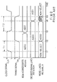
- a typical example of an addressing system largely comprises an address buffer unit 1, an address decoder unit 2, a word line driver unit 3, and a timing control unit 4.
- External row address bits A0 to Ax are supplied to the address buffer unit 1, and are latched therein in response to a clock signal CLk of low voltage level.
- CLk clock signal
- the address buffer unit 1 is coupled through address signal lines A0, CA0, Ax and CAx with the address decoder unit 2, and the address decoder unit 2 is constituted by a plurality of address decoder circuits 21 to 2m selectively coupled with the address signal lines A0, CA0, Ax and CAx.
- the address decoder circuits 21 to 2m are identical in circuit arrangement with one another, and each of the address decoder circuits 21 to 2m is implemented by a series combination of a NAND gate NA1 and an inverter IV1.
- the address decoder unit 2 is coupled through decoded signal lines XS1 to XSm with the word line driver unit 3, and the word line driver unit 3 is constituted by a plurality of word line driver circuits 31 to 3m associated with word lines WL1 to WLm, respectively. All of the word line driver circuits 31 to 3m are identical in circuit arrangement with one another, and each of the word line driver circuits 31 to 3m comprises a series combination of a NAND gate NA2 and an inverter IV2.
- the timing control unit 4 produces a timing signal TM shifting the voltage level thereof in synchronism with the clock signal CLK.
- the NAND data NA2 is coupled with the timing control unit 4 as well as with the associated decoded signal line, and is enabled with the clock signal CLK of logic "1" level.
- the inverter IV2 drives the associated word line to active high voltage level when the external row address bits A0 to Ax are indicative of a row address assigned to the associated word line.
- the prior art addressing system thus arranged behaves as follows. Assuming now that the external address bits A0 to Ax are indicative of the address assigned to the word line WL1, the row address bits A0 to Ax are latched with the clock signal CLK of the low voltage level, and the clock signal CLK of the low voltage level disables the NAND gates of the word line driver circuits 31 to 3m. For this reason, all of the word lines WL1 to WLm go down to the inactive low voltage level.
- the address buffer unit 1 selectively drives the address signal lines A0, CA0, Ax and CAx, and address decoder circuits 21 is responsive to the logic levels on the address signal lines A0, CA0, Ax and CAx. Namely, the NAND gate NA1 shifts the output node thereof to logic "0" level, and the inverter IV1 drives the decoded signal line XS1 to logic "1" level.
- the address buffer unit keeps the row address bits A0 to Ax, and the timing control unit 4 shifts the timing signal TM to the high voltage level or logic "1" level. Then, the word line driver circuits 31 to 3m are enabled, and the NAND gate NA2 shifts the output node to logic "0" level. As a result, the inverter IV2 drives the associated word line WL1 to the active high voltage level, and the other word line driver circuits keep the associated word lines in the inactive low voltage level.
- the time lag in the timing control unit 4 is expected to be designed as small as possible. It is effective against time delay to minimize the time lag with respect to the leading edge of the clock pulse CLK. However, the timing control unit 4 tends to increase time lag to the trailing edge one and a half times longer than the time lag to the leading edge. Assuming now that the duty ratio of the clock signal CLK is 50 per cent, the timing control signal 4 introduces time delay T1 between the leading edge of the clock signal CLK and leading edge of the timing signal TM and time delay T2 between the trailing edge of the clock signal CLK and the trailing edge of the timing signal TM as shown in Fig.
- the time delay T2 is one and a half times longer than the time delay T1.
- the pulse width of the timing signal TM is prolonged.
- the row address ADD0 indicated by the row address bits A0 to Ax has been latched before time t1, and one of the row address decoder circuits 21 to 2m drives the associated decoded signal line until time t4. For this reason, the word line assigned the row address ADD0 is driven to the active high voltage level at time t4, and the associated word line driver circuit continues to drive this word line until time t5, because the prolonged timing signal TM remains in the high voltage level.
- the clock signal CLK is recovered from the high voltage level to the low voltage level at time t3, and the address buffer unit 1 latches a new row address bits indicative of a row address ADD1.
- another address decoder circuit drives the associated decoded signal line to the active high voltage level at time t4
- another word line driver circuit drives the word line assigned the row address ADD1 to the active high voltage level at time t4.
- multi-selection takes place between time t4 and time t5, and, accordingly, the two word lines are in the active high voltage level.
- Such a simultaneous selection is not desirable, because two data bits are read out from two memory cells respectively coupled with the two word lines. The two data bits on a bit line pair are interfered with each other, and are liable to be destroyed.
- the present invention proposes to forcibly shift all of address lines while an in-phase timing signal remains in a first level.
- an addressing system associated with a plurality of address lines respectively assigned addresses, comprising: a) an address buffer unit responsive to a clock signal of a first level for latching an address signal indicative of one of the addresses, and storing the address signal when the clock signal is shifted from the first level to a second level, the address buffer unit maintaining the address signal until the clock signal is shifted to the first level again; b) an address decoder unit coupled with the address buffer unit for selectively driving decoded signal lines; c) a timing control unit responsive to the clock signal for producing an in-phase timing signal; and d) a driver unit having a plurality of driver circuits respectively coupled between the decoded signal lines and the plurality of address lines, the plurality of driver circuits being operative to respectively latch logic levels on the associated decoded signal lines when the in-phase timing signal is shifted from the first level to the second level so as to selectively drive the address lines to active level, the plurality of driver circuits maintaining all of the address lines in
- a semiconductor memory device comprises a memory cell array 1, and an addressing system.
- the memory cell array 1 is constituted by a plurality of memory cells M11, M1n, Mm1 and Mmn arranged in rows and columns, and the addressing system selects a memory cell from the memory cell array 1.
- a plurality of word lines WL1 to WLm are respectively associated with the rows of the memory cells M11 to Mmn, and row addresses are respectively assigned to the word lines WL1 to WLm. In this instance, the word lines WL1 to WLm serve as address lines.
- a plurality of bit line pairs BL1 to BLn are further associated with the columns of the memory cells M11 to Mmn, and column addresses are respectively assigned to the bit line pairs BL1 to BLn.
- word lines WL1 to WLm and the digit line pairs BL1 to BLn With the word lines WL1 to WLm and the digit line pairs BL1 to BLn, one of the memory cells M11 to Mmn is addressable, and a data bit stored therein is accessed.
- the addressing system largely comprises an address buffer unit 11, an address decoder unit 12, a word line driver unit 13, and a timing control unit 14. External row address bits A0 to Ax are supplied to the address buffer unit 11, and are latched therein in response to a clock signal CLk of low voltage level. In this instance, the duty ratio of the clock signal CLK is assumed to be 50 per cent.
- the address buffer unit 11 is coupled through address signal lines A0, CAO, Ax and CAx with the address decoder unit 12, and the address decoder unit 12 is constituted by a plurality of address decoder circuits 121 to 12m selectively coupled with the address signal lines A0, CA0, Ax and CAx.
- the address decoder circuits 121 to 12m are identical in circuit arrangement with one another, and each of the address decoder circuits 121 to 12m is implemented by a series combination of a NAND gate NA11 and an inverter IV11.
- the address decoder unit 12 is coupled through decoded signal lines XS1 to XSm with the word line driver unit 13, and the word line driver unit 13 is constituted by a plurality of clocked flip flop circuits 131 to 13m associated with word lines WL1 to WLm, respectively.
- the clocked flip flop circuit 131, ... or 13m has a data input node D coupled with the associated decoded signal line XS1, ...
- the timing control unit 14 produces a timing signal TM shifting the voltage level thereof in synchronism with the clock signal CLK, and, accordingly, the timing signal TM is the in-phase signal of the clock signal CLK.
- the timing control unit 14 introduce longer time lag between the trailing edge of the clock signal CLK and the trailing edge of the timing signal TM rather than the leading edge of the clock signal CLK and the leading edge of the timing signal TM, and, for this reason, prolongs the pulse width of the timing signal TM.
- the timing control signal TM goes up to the high voltage level, and the clocked flip flop circuit 131 shifts the data output node Q and the word line WL1 to the active high voltage level in accordance with the voltage level on the decoded signal line XS1.
- the row address bits A0 to Ax are changed and indicates the row address ADD1 at time t13.
- the new row address ADD1 is latched by the address buffer unit 11 upon pull-down of the clock signal CLK at time t14, and the address decoder circuit 12m shifts the associated decoded signal line XSm to the high voltage level instead of the decoded signal line XS1.
- the timing signal TM of the high voltage level causes the flip flop circuits 131 to 13m to keep the previous voltage level at the output nodes Q thereof, and no multi-selection takes place between time t15 and time t16.
- the timing signal TM goes down to the low voltage level, and all of the clocked flip flop circuits 131 to 13m enter the reset state. As a result, all of the word lines WL1 to WLm go down to the inactive low voltage level. If the timing signal TM goes up to the high voltage level at time t17 again, the clocked flip flop circuit 13m drives the word line WLm to the active high voltage level.
- the addressing system allows all of the flip flop circuits 131 to 13m to enter the reset state before selectively driving the word lines WL1 to WLm, and no multi-selection takes place, thereby preventing the data bits stored in the memory cell array 10 from destruction.
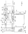
- FIG. 5 of the drawings another addressing system embodying the present invention is similar in circuit arrangement to the first embodiment except for an address decoder unit 22 and a driver unit 23, and the other component circuits and signal lines are labeled with the same references designating the corresponding circuits and signal lines of the first embodiment without detailed description for the sake of simplicity.
- the address decoder unit 22 is constituted by NAND gates 221 to 22m selectively coupled with the address lines A0, CA0, Ax and CAx, and the driver unit 23 is constituted by a plurality of driver circuits 231 to 23m. All of the driver circuits 231 to 23m are similar in circuit arrangement to one another, and each driver circuit comprises a latch circuit 24 and a logic circuit 25.
- the latch circuit 24 comprises a p-channel enhancement type transfer transistor 24a, and a flip flop circuit 24b implemented by two inverters, and the timing signal TM is supplied to the gate electrode of the p-channel enhancement type transfer transistor 24a.
- the logic circuit 25 is implemented by a series combination of a NAND gate 25a and an inverter 25b, and the inverter 25b drives the associated word line.
- the output node of the latch circuit 24 is coupled with one of the input nodes of the NAND gate 25a, and the timing signal TM is supplied to the other input node of the NAND gate 25a.
- the driver circuit 231, ... or 23m behaves as follows. While the timing signal TM remains in the low voltage level, the p-channel enhancement type transfer transistor 24a turns on for transferring the logic level on the associated decoded signal line to the associated flip flop circuit 24b, and the NAND gate 25a is disabled so that the associated word line goes down to the inactive low voltage level. On the other hand, if the timing signal TM goes up to the high voltage level, the flip flop circuit 24b is isolated from the associated decoded signal line, and the NAND gate 25a is enabled so as to be responsive to the logic level at the output node of the flip flop circuit 24b.
- the driver unit 23 forcibly shifts all of the word lines WL1 to WLm before selectively driving the word lines WL1 to WLm, and no multi-selection takes place.
- the addressing system according to the present invention may be available for any type of a semiconductor memory device such as, for example, a dynamic random access memory device, a static random access memory device, a read only memory device and so forth.
Landscapes
- Engineering & Computer Science (AREA)
- Microelectronics & Electronic Packaging (AREA)
- Static Random-Access Memory (AREA)
- Dram (AREA)
Abstract
Description
- This invention relates to a semiconductor memory device and, more particularly, to an addressing system incorporated in the semiconductor memory device.
- Referring first to Fig. 1 of the drawings, a typical example of an addressing system largely comprises an
address buffer unit 1, an address decoder unit 2, a wordline driver unit 3, and atiming control unit 4. External row address bits A0 to Ax are supplied to theaddress buffer unit 1, and are latched therein in response to a clock signal CLk of low voltage level. In the following description, the low level corresponds to logic "0" level, and high voltage level is equivalent to logic "1" level. Theaddress buffer unit 1 is coupled through address signal lines A0, CA0, Ax and CAx with the address decoder unit 2, and the address decoder unit 2 is constituted by a plurality of address decoder circuits 21 to 2m selectively coupled with the address signal lines A0, CA0, Ax and CAx. The address decoder circuits 21 to 2m are identical in circuit arrangement with one another, and each of the address decoder circuits 21 to 2m is implemented by a series combination of a NAND gate NA1 and an inverter IV1. The address decoder unit 2 is coupled through decoded signal lines XS1 to XSm with the wordline driver unit 3, and the wordline driver unit 3 is constituted by a plurality of wordline driver circuits 31 to 3m associated with word lines WL1 to WLm, respectively. All of the wordline driver circuits 31 to 3m are identical in circuit arrangement with one another, and each of the wordline driver circuits 31 to 3m comprises a series combination of a NAND gate NA2 and an inverter IV2. Thetiming control unit 4 produces a timing signal TM shifting the voltage level thereof in synchronism with the clock signal CLK. The NAND data NA2 is coupled with thetiming control unit 4 as well as with the associated decoded signal line, and is enabled with the clock signal CLK of logic "1" level. The inverter IV2 drives the associated word line to active high voltage level when the external row address bits A0 to Ax are indicative of a row address assigned to the associated word line. - The prior art addressing system thus arranged behaves as follows. Assuming now that the external address bits A0 to Ax are indicative of the address assigned to the word line WL1, the row address bits A0 to Ax are latched with the clock signal CLK of the low voltage level, and the clock signal CLK of the low voltage level disables the NAND gates of the word
line driver circuits 31 to 3m. For this reason, all of the word lines WL1 to WLm go down to the inactive low voltage level. Theaddress buffer unit 1 selectively drives the address signal lines A0, CA0, Ax and CAx, and address decoder circuits 21 is responsive to the logic levels on the address signal lines A0, CA0, Ax and CAx. Namely, the NAND gate NA1 shifts the output node thereof to logic "0" level, and the inverter IV1 drives the decoded signal line XS1 to logic "1" level. - When the clock signal CLK goes up to the high voltage level, the address buffer unit keeps the row address bits A0 to Ax, and the
timing control unit 4 shifts the timing signal TM to the high voltage level or logic "1" level. Then, the wordline driver circuits 31 to 3m are enabled, and the NAND gate NA2 shifts the output node to logic "0" level. As a result, the inverter IV2 drives the associated word line WL1 to the active high voltage level, and the other word line driver circuits keep the associated word lines in the inactive low voltage level. - Users request the manufacturer to speed up the data access, and the time lag in the
timing control unit 4 is expected to be designed as small as possible. It is effective against time delay to minimize the time lag with respect to the leading edge of the clock pulse CLK. However, thetiming control unit 4 tends to increase time lag to the trailing edge one and a half times longer than the time lag to the leading edge. Assuming now that the duty ratio of the clock signal CLK is 50 per cent, thetiming control signal 4 introduces time delay T1 between the leading edge of the clock signal CLK and leading edge of the timing signal TM and time delay T2 between the trailing edge of the clock signal CLK and the trailing edge of the timing signal TM as shown in Fig. 2, and the time delay T2 is one and a half times longer than the time delay T1. In other words, the pulse width of the timing signal TM is prolonged. The row address ADD0 indicated by the row address bits A0 to Ax has been latched before time t1, and one of the row address decoder circuits 21 to 2m drives the associated decoded signal line until time t4. For this reason, the word line assigned the row address ADD0 is driven to the active high voltage level at time t4, and the associated word line driver circuit continues to drive this word line until time t5, because the prolonged timing signal TM remains in the high voltage level. However, the clock signal CLK is recovered from the high voltage level to the low voltage level at time t3, and theaddress buffer unit 1 latches a new row address bits indicative of a row address ADD1. For this reason, another address decoder circuit drives the associated decoded signal line to the active high voltage level at time t4, and another word line driver circuit drives the word line assigned the row address ADD1 to the active high voltage level at time t4. Then, multi-selection takes place between time t4 and time t5, and, accordingly, the two word lines are in the active high voltage level. Such a simultaneous selection is not desirable, because two data bits are read out from two memory cells respectively coupled with the two word lines. The two data bits on a bit line pair are interfered with each other, and are liable to be destroyed. - It is therefore an important object of the present invention to provide an addressing system which is free from multi-selection.
- To accomplish the object, the present invention proposes to forcibly shift all of address lines while an in-phase timing signal remains in a first level.
- In accordance with the present invention, there is provided an addressing system associated with a plurality of address lines respectively assigned addresses, comprising: a) an address buffer unit responsive to a clock signal of a first level for latching an address signal indicative of one of the addresses, and storing the address signal when the clock signal is shifted from the first level to a second level, the address buffer unit maintaining the address signal until the clock signal is shifted to the first level again; b) an address decoder unit coupled with the address buffer unit for selectively driving decoded signal lines; c) a timing control unit responsive to the clock signal for producing an in-phase timing signal; and d) a driver unit having a plurality of driver circuits respectively coupled between the decoded signal lines and the plurality of address lines, the plurality of driver circuits being operative to respectively latch logic levels on the associated decoded signal lines when the in-phase timing signal is shifted from the first level to the second level so as to selectively drive the address lines to active level, the plurality of driver circuits maintaining all of the address lines in inactive level while the in-phase timing signal remains in the first level.
- The features and advantages of the addressing system according to the present invention will be more clearly understood from the following description taken in conjunction with the accompanying drawings in which:
- Fig. 1 is a block diagram showing the circuit arrangement of the prior art addressing system;
- Fig. 2 is a timing chart showing the multi-selection in the prior art addressing system;
- Fig. 3 is a block diagram showing the circuit arrangement of an essential part of a semiconductor memory device equipped with an addressing system according to the present invention;
- Fig. 4 is a timing chart showing the circuit behavior of the addressing system according to the present invention; and
- Fig. 5 is a block diagram showing the circuit arrangement of another addressing system according to the present invention.
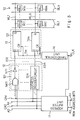
- Referring to Fig. 3, a semiconductor memory device comprises a
memory cell array 1, and an addressing system. Thememory cell array 1 is constituted by a plurality of memory cells M11, M1n, Mm1 and Mmn arranged in rows and columns, and the addressing system selects a memory cell from thememory cell array 1. A plurality of word lines WL1 to WLm are respectively associated with the rows of the memory cells M11 to Mmn, and row addresses are respectively assigned to the word lines WL1 to WLm. In this instance, the word lines WL1 to WLm serve as address lines. A plurality of bit line pairs BL1 to BLn are further associated with the columns of the memory cells M11 to Mmn, and column addresses are respectively assigned to the bit line pairs BL1 to BLn. With the word lines WL1 to WLm and the digit line pairs BL1 to BLn, one of the memory cells M11 to Mmn is addressable, and a data bit stored therein is accessed. - The addressing system according to the present invention largely comprises an
address buffer unit 11, anaddress decoder unit 12, a wordline driver unit 13, and atiming control unit 14. External row address bits A0 to Ax are supplied to theaddress buffer unit 11, and are latched therein in response to a clock signal CLk of low voltage level. In this instance, the duty ratio of the clock signal CLK is assumed to be 50 per cent. Theaddress buffer unit 11 is coupled through address signal lines A0, CAO, Ax and CAx with theaddress decoder unit 12, and theaddress decoder unit 12 is constituted by a plurality ofaddress decoder circuits 121 to 12m selectively coupled with the address signal lines A0, CA0, Ax and CAx. Theaddress decoder circuits 121 to 12m are identical in circuit arrangement with one another, and each of theaddress decoder circuits 121 to 12m is implemented by a series combination of a NAND gate NA11 and an inverter IV11. Theaddress decoder unit 12 is coupled through decoded signal lines XS1 to XSm with the wordline driver unit 13, and the wordline driver unit 13 is constituted by a plurality of clockedflip flop circuits 131 to 13m associated with word lines WL1 to WLm, respectively. The clockedflip flop circuit 131, ... or 13m has a data input node D coupled with the associated decoded signal line XS1, ... or XSm, a clocked node C coupled with the output node of thetiming control unit 14, a reset node CR also coupled with the output node of thetiming control unit 14, and an output node Q coupled with the associated word line WL1, ... or WLm. Thetiming control unit 14 produces a timing signal TM shifting the voltage level thereof in synchronism with the clock signal CLK, and, accordingly, the timing signal TM is the in-phase signal of the clock signal CLK. Thetiming control unit 14 introduce longer time lag between the trailing edge of the clock signal CLK and the trailing edge of the timing signal TM rather than the leading edge of the clock signal CLK and the leading edge of the timing signal TM, and, for this reason, prolongs the pulse width of the timing signal TM. - Description is hereinbelow made on circuit behavior of the semiconductor memory device with reference to Fig. 4 on the assumption that row addresses ADD0 and ADD1 are respectively assigned to the word lines WL1 and WLm. The row address bits A0 to Ax are indicative of the row address ADD0 before time t11, and have been latched by the
address buffer unit 11. Even if theaddress decoder circuit 121 has shifted the decoded signal line XS1 to the high voltage level corresponding to logic "1" level before time t11, the clockedflip flop circuit 131 causes the word line WL1 to remain in the inactive low voltage level, because the timing signal TM remains in the low voltage level. At time t12, the timing control signal TM goes up to the high voltage level, and the clockedflip flop circuit 131 shifts the data output node Q and the word line WL1 to the active high voltage level in accordance with the voltage level on the decoded signal line XS1. - The row address bits A0 to Ax are changed and indicates the row address ADD1 at time t13. The new row address ADD1 is latched by the
address buffer unit 11 upon pull-down of the clock signal CLK at time t14, and theaddress decoder circuit 12m shifts the associated decoded signal line XSm to the high voltage level instead of the decoded signal line XS1. However, the timing signal TM of the high voltage level causes theflip flop circuits 131 to 13m to keep the previous voltage level at the output nodes Q thereof, and no multi-selection takes place between time t15 and time t16. At time t16, the timing signal TM goes down to the low voltage level, and all of the clockedflip flop circuits 131 to 13m enter the reset state. As a result, all of the word lines WL1 to WLm go down to the inactive low voltage level. If the timing signal TM goes up to the high voltage level at time t17 again, the clockedflip flop circuit 13m drives the word line WLm to the active high voltage level. - Thus, the addressing system according to the present invention allows all of the
flip flop circuits 131 to 13m to enter the reset state before selectively driving the word lines WL1 to WLm, and no multi-selection takes place, thereby preventing the data bits stored in thememory cell array 10 from destruction. - Turning to Fig. 5 of the drawings, another addressing system embodying the present invention is similar in circuit arrangement to the first embodiment except for an
address decoder unit 22 and adriver unit 23, and the other component circuits and signal lines are labeled with the same references designating the corresponding circuits and signal lines of the first embodiment without detailed description for the sake of simplicity. - The
address decoder unit 22 is constituted byNAND gates 221 to 22m selectively coupled with the address lines A0, CA0, Ax and CAx, and thedriver unit 23 is constituted by a plurality ofdriver circuits 231 to 23m. All of thedriver circuits 231 to 23m are similar in circuit arrangement to one another, and each driver circuit comprises alatch circuit 24 and alogic circuit 25. Thelatch circuit 24 comprises a p-channel enhancementtype transfer transistor 24a, and aflip flop circuit 24b implemented by two inverters, and the timing signal TM is supplied to the gate electrode of the p-channel enhancementtype transfer transistor 24a. Thelogic circuit 25 is implemented by a series combination of aNAND gate 25a and aninverter 25b, and theinverter 25b drives the associated word line. The output node of thelatch circuit 24 is coupled with one of the input nodes of theNAND gate 25a, and the timing signal TM is supplied to the other input node of theNAND gate 25a. - The
driver circuit 231, ... or 23m thus arranged behaves as follows. While the timing signal TM remains in the low voltage level, the p-channel enhancementtype transfer transistor 24a turns on for transferring the logic level on the associated decoded signal line to the associatedflip flop circuit 24b, and theNAND gate 25a is disabled so that the associated word line goes down to the inactive low voltage level. On the other hand, if the timing signal TM goes up to the high voltage level, theflip flop circuit 24b is isolated from the associated decoded signal line, and theNAND gate 25a is enabled so as to be responsive to the logic level at the output node of theflip flop circuit 24b. - Thus, the
driver unit 23 forcibly shifts all of the word lines WL1 to WLm before selectively driving the word lines WL1 to WLm, and no multi-selection takes place. - Although particular embodiments of the present invention have been shown and described, it will be obvious to those skilled in the art that various changes and modifications may be made without departing from the spirit and scope of the present invention. For example, the addressing system according to the present invention may be available for any type of a semiconductor memory device such as, for example, a dynamic random access memory device, a static random access memory device, a read only memory device and so forth.
Claims (5)
- An addressing system associated with a plurality of address lines (WL1 to WLm) respectively assigned addresses, comprising:a) an address buffer unit (11) responsive to a clock signal (CLK) of a first level (L) for latching an address signal (A0 to Ax) indicative of one of said addresses, and storing said address signal when said clock signal is shifted from said first level to a second level (H), said address buffer unit maintaining said address signal until said clock signal is shifted to the first level again;b) an address decoder unit (12; 22) coupled with said address buffer unit for selectively driving decoded signal lines (XS1 to XSm);c) a timing control unit (14) responsive to said clock signal for producing an in-phase timing signal (TM); andd) a driver unit (13; 23) having a plurality of driver circuits (131 to 13m; 231 to 23m) respectively coupled between said decoded signal lines and said plurality of address lines,characterized in that
said plurality of driver circuits are operative to respectively latch logic levels on the associated decoded signal lines when said in-phase timing signal is shifted from said first level to said second level so as to selectively drive said address lines to active level, said plurality of driver circuits maintaining all of said address lines in inactive level while said in-phase timing signal remains in said first level. - An addressing system as set forth in claim 1, in which each of said driver circuits (131 to 13m) is implemented by a flip flop circuit having a data input node (D) coupled with the associated decoded signal line, an data output node (Q) coupled with the associated address line, a clock node (C) responsive to said in-phase timing signal of said second level for matching a logic level on said associated address line with the logic level on said associated address line, and a reset node (CR) responsive to said in-phase timing signal of said first level for forcibly shifting said data output node to said inactive level.
- An addressing system as set forth in claim 1, in which each of said plurality of driver circuits (231 to 23m) comprises a latch circuit (24) responsive to said in-phase timing signal of said first level for storing the logic level on said associated decoded signal line, and isolated from said associated decoded signal line in the presence of said in-phase timing signal of said second level, and a logic circuit (25) coupled between said latch circuit and the associated address line, and enabled with said in-phase timing signal of said second level.
- An addressing system as set forth in claim 3, in which said latch circuit (24) comprises a transfer transistor (24a) coupled with the associated decoded signal line and gated with said in-phase timing signal, and a flip flop circuit (24b) coupled between said transfer transistor and said associated logic circuit.
- An addressing system as set forth in claim 4, in which said logic circuit (25) comprises a HAND gate (25a) having a first input node supplied with said in-phase timing signal and a second input node coupled with said flip flop circuit, and an inverter (25b) coupled between said NAND gate and said associated address line.
Applications Claiming Priority (2)
| Application Number | Priority Date | Filing Date | Title |
|---|---|---|---|
| JP3235776A JPH0574167A (en) | 1991-09-17 | 1991-09-17 | Semiconductor memory device |
| JP235776/91 | 1991-09-17 |
Publications (3)
| Publication Number | Publication Date |
|---|---|
| EP0533096A2 true EP0533096A2 (en) | 1993-03-24 |
| EP0533096A3 EP0533096A3 (en) | 1995-04-19 |
| EP0533096B1 EP0533096B1 (en) | 1997-05-28 |
Family
ID=16991075
Family Applications (1)
| Application Number | Title | Priority Date | Filing Date |
|---|---|---|---|
| EP92115720A Expired - Lifetime EP0533096B1 (en) | 1991-09-17 | 1992-09-14 | Addressing system free from multi-selection of word lines |
Country Status (4)
| Country | Link |
|---|---|
| US (1) | US5295115A (en) |
| EP (1) | EP0533096B1 (en) |
| JP (1) | JPH0574167A (en) |
| DE (1) | DE69219971T2 (en) |
Cited By (5)
| Publication number | Priority date | Publication date | Assignee | Title |
|---|---|---|---|---|
| US5598375A (en) * | 1995-06-23 | 1997-01-28 | Electronics Research & Service Organization | Static random access memory dynamic address decoder with non-overlap word-line enable |
| EP0793235A2 (en) * | 1996-02-28 | 1997-09-03 | Nec Corporation | Single-chip memory system having a decoder for pulse word line method |
| WO2004006261A2 (en) * | 2002-07-02 | 2004-01-15 | Advanced Micro Devices, Inc. | Wordline latching in semiconductor memories |
| WO2005013282A1 (en) * | 2003-07-02 | 2005-02-10 | Advanced Micro Devices, Inc. | Wordline latching in semiconductor memories |
| US6876592B2 (en) | 2000-03-08 | 2005-04-05 | Nec Electronics Corporation | Semiconductor memory device |
Families Citing this family (18)
| Publication number | Priority date | Publication date | Assignee | Title |
|---|---|---|---|---|
| US6249481B1 (en) | 1991-10-15 | 2001-06-19 | Kabushiki Kaisha Toshiba | Semiconductor memory device |
| JP2740063B2 (en) * | 1990-10-15 | 1998-04-15 | 株式会社東芝 | Semiconductor storage device |
| EP0561370B1 (en) * | 1992-03-19 | 1999-06-02 | Kabushiki Kaisha Toshiba | A clock-synchronous semiconductor memory device and access method thereof |
| US6310821B1 (en) * | 1998-07-10 | 2001-10-30 | Kabushiki Kaisha Toshiba | Clock-synchronous semiconductor memory device and access method thereof |
| JP2739809B2 (en) * | 1993-07-30 | 1998-04-15 | 日本電気株式会社 | Semiconductor integrated circuit |
| US5493530A (en) * | 1993-08-26 | 1996-02-20 | Paradigm Technology, Inc. | Ram with pre-input register logic |
| JP3157681B2 (en) * | 1994-06-27 | 2001-04-16 | 日本電気株式会社 | Logical data input latch circuit |
| JPH0946232A (en) * | 1995-07-28 | 1997-02-14 | Nec Corp | Decoding device |
| US5822252A (en) * | 1996-03-29 | 1998-10-13 | Aplus Integrated Circuits, Inc. | Flash memory wordline decoder with overerase repair |
| DE19830111A1 (en) * | 1998-07-06 | 2000-01-13 | Siemens Ag | Integrated memory |
| KR100326268B1 (en) * | 1998-10-28 | 2002-05-09 | 박종섭 | Decoding device for taking driving margin at decoding and its method |
| US6366524B1 (en) * | 2000-07-28 | 2002-04-02 | Micron Technology Inc. | Address decoding in multiple-bank memory architectures |
| KR100408720B1 (en) * | 2001-06-28 | 2003-12-11 | 주식회사 하이닉스반도체 | Decoder circuit of semiconductor memory device |
| US6873567B2 (en) * | 2002-08-09 | 2005-03-29 | International Business Machines Corporation | Device and method for decoding an address word into word-line signals |
| US7263024B2 (en) * | 2005-10-17 | 2007-08-28 | Lattice Semiconductor Corporation | Clock reset address decoder for block memory |
| JP2014116054A (en) * | 2012-12-12 | 2014-06-26 | Nec Corp | Integrated circuit |
| US9159391B1 (en) * | 2012-12-13 | 2015-10-13 | Gsi Technology, Inc. | Systems and methods of double/quad data rate memory involving input latching, self-timing and/or other features |
| US9431079B1 (en) | 2012-12-13 | 2016-08-30 | Gsi Technology, Inc. | Systems and methods of memory and memory operation involving input latching, self-timing and/or other features |
Citations (3)
| Publication number | Priority date | Publication date | Assignee | Title |
|---|---|---|---|---|
| EP0098164A2 (en) * | 1982-06-30 | 1984-01-11 | Fujitsu Limited | Static type semiconductor memory device |
| EP0142376A2 (en) * | 1983-11-16 | 1985-05-22 | Fujitsu Limited | Dynamic random access memory |
| US4833656A (en) * | 1986-11-11 | 1989-05-23 | Mitsubishi Denki Kabushiki Kaisha | Fast access circuit for dynamic type semiconductor memory device |
Family Cites Families (2)
| Publication number | Priority date | Publication date | Assignee | Title |
|---|---|---|---|---|
| US5086414A (en) * | 1988-11-17 | 1992-02-04 | Hitachi, Ltd. | Semiconductor device having latch means |
| US5107465A (en) * | 1989-09-13 | 1992-04-21 | Advanced Micro Devices, Inc. | Asynchronous/synchronous pipeline dual mode memory access circuit and method |
-
1991
- 1991-09-17 JP JP3235776A patent/JPH0574167A/en active Pending
-
1992
- 1992-09-14 EP EP92115720A patent/EP0533096B1/en not_active Expired - Lifetime
- 1992-09-14 DE DE69219971T patent/DE69219971T2/en not_active Expired - Fee Related
- 1992-09-16 US US07/945,610 patent/US5295115A/en not_active Expired - Fee Related
Patent Citations (3)
| Publication number | Priority date | Publication date | Assignee | Title |
|---|---|---|---|---|
| EP0098164A2 (en) * | 1982-06-30 | 1984-01-11 | Fujitsu Limited | Static type semiconductor memory device |
| EP0142376A2 (en) * | 1983-11-16 | 1985-05-22 | Fujitsu Limited | Dynamic random access memory |
| US4833656A (en) * | 1986-11-11 | 1989-05-23 | Mitsubishi Denki Kabushiki Kaisha | Fast access circuit for dynamic type semiconductor memory device |
Cited By (9)
| Publication number | Priority date | Publication date | Assignee | Title |
|---|---|---|---|---|
| US5598375A (en) * | 1995-06-23 | 1997-01-28 | Electronics Research & Service Organization | Static random access memory dynamic address decoder with non-overlap word-line enable |
| EP0793235A2 (en) * | 1996-02-28 | 1997-09-03 | Nec Corporation | Single-chip memory system having a decoder for pulse word line method |
| EP0793235A3 (en) * | 1996-02-28 | 2000-03-15 | Nec Corporation | Single-chip memory system having a decoder for pulse word line method |
| US6876592B2 (en) | 2000-03-08 | 2005-04-05 | Nec Electronics Corporation | Semiconductor memory device |
| WO2004006261A2 (en) * | 2002-07-02 | 2004-01-15 | Advanced Micro Devices, Inc. | Wordline latching in semiconductor memories |
| WO2004006261A3 (en) * | 2002-07-02 | 2004-04-15 | Advanced Micro Devices Inc | Wordline latching in semiconductor memories |
| US6798712B2 (en) | 2002-07-02 | 2004-09-28 | Advanced Micro Devices, Inc. | Wordline latching in semiconductor memories |
| KR100984373B1 (en) * | 2002-07-02 | 2010-09-30 | 어드밴스드 마이크로 디바이시즈, 인코포레이티드 | System and method including worldline latching in semiconductor memories |
| WO2005013282A1 (en) * | 2003-07-02 | 2005-02-10 | Advanced Micro Devices, Inc. | Wordline latching in semiconductor memories |
Also Published As
| Publication number | Publication date |
|---|---|
| EP0533096A3 (en) | 1995-04-19 |
| DE69219971D1 (en) | 1997-07-03 |
| DE69219971T2 (en) | 1997-12-18 |
| EP0533096B1 (en) | 1997-05-28 |
| JPH0574167A (en) | 1993-03-26 |
| US5295115A (en) | 1994-03-15 |
Similar Documents
| Publication | Publication Date | Title |
|---|---|---|
| EP0533096B1 (en) | Addressing system free from multi-selection of word lines | |
| US5155705A (en) | Semiconductor memory device having flash write function | |
| US4905192A (en) | Semiconductor memory cell | |
| EP0347530B1 (en) | Static random access memory device with a power dissipation reduction function | |
| US5003510A (en) | Semiconductor memory device with flash write mode of operation | |
| US6646938B2 (en) | Static memory having self-timing circuit | |
| US5532961A (en) | Semiconductor memory device having extended data out function | |
| EP0186906B1 (en) | Semiconductor memory attaining high data read speed and having high noise margin | |
| KR100328161B1 (en) | Integrated circuit memory | |
| US20010037429A1 (en) | Balanced switching method and circuit | |
| EP0213395A2 (en) | Semiconductor memory with static column decode and page mode addressing capability | |
| US5047983A (en) | Semiconductor storage device with redundancy arrangement | |
| EP0467607B1 (en) | Semiconductor memory device | |
| US5357479A (en) | Static random access memory capable of preventing erroneous writing | |
| US6212094B1 (en) | Low power SRAM memory cell having a single bit line | |
| US5493536A (en) | Dual-port random access memory having memory cell controlled by write data lines and read enable line | |
| US5455795A (en) | Semiconductor memory device | |
| KR0136448B1 (en) | Semiconductor memory device with error self-correction function | |
| JP3317746B2 (en) | Semiconductor storage device | |
| US4858188A (en) | Semiconductor memory with improved write function | |
| US5359559A (en) | Semiconductor memory device having redundant memory cells | |
| US5461593A (en) | Word-line driver for a semiconductor memory device | |
| KR910014938A (en) | Integrated Circuit Memory with Enhanced DI / DT Control | |
| JP2607799B2 (en) | Memory device | |
| US5365482A (en) | Semiconductor memory device with provision of pseudo-acceleration test |
Legal Events
| Date | Code | Title | Description |
|---|---|---|---|
| PUAI | Public reference made under article 153(3) epc to a published international application that has entered the european phase |
Free format text: ORIGINAL CODE: 0009012 |
|
| AK | Designated contracting states |
Kind code of ref document: A2 Designated state(s): DE FR GB |
|
| PUAL | Search report despatched |
Free format text: ORIGINAL CODE: 0009013 |
|
| AK | Designated contracting states |
Kind code of ref document: A3 Designated state(s): DE FR GB |
|
| 17P | Request for examination filed |
Effective date: 19950314 |
|
| GRAG | Despatch of communication of intention to grant |
Free format text: ORIGINAL CODE: EPIDOS AGRA |
|
| 17Q | First examination report despatched |
Effective date: 19960722 |
|
| GRAH | Despatch of communication of intention to grant a patent |
Free format text: ORIGINAL CODE: EPIDOS IGRA |
|
| GRAH | Despatch of communication of intention to grant a patent |
Free format text: ORIGINAL CODE: EPIDOS IGRA |
|
| GRAA | (expected) grant |
Free format text: ORIGINAL CODE: 0009210 |
|
| AK | Designated contracting states |
Kind code of ref document: B1 Designated state(s): DE FR GB |
|
| REF | Corresponds to: |
Ref document number: 69219971 Country of ref document: DE Date of ref document: 19970703 |
|
| ET | Fr: translation filed | ||
| PLBE | No opposition filed within time limit |
Free format text: ORIGINAL CODE: 0009261 |
|
| STAA | Information on the status of an ep patent application or granted ep patent |
Free format text: STATUS: NO OPPOSITION FILED WITHIN TIME LIMIT |
|
| 26N | No opposition filed | ||
| PGFP | Annual fee paid to national office [announced via postgrant information from national office to epo] |
Ref country code: FR Payment date: 20010911 Year of fee payment: 10 |
|
| PGFP | Annual fee paid to national office [announced via postgrant information from national office to epo] |
Ref country code: GB Payment date: 20010912 Year of fee payment: 10 |
|
| PGFP | Annual fee paid to national office [announced via postgrant information from national office to epo] |
Ref country code: DE Payment date: 20011001 Year of fee payment: 10 |
|
| REG | Reference to a national code |
Ref country code: GB Ref legal event code: IF02 |
|
| PG25 | Lapsed in a contracting state [announced via postgrant information from national office to epo] |
Ref country code: GB Free format text: LAPSE BECAUSE OF NON-PAYMENT OF DUE FEES Effective date: 20020914 |
|
| PG25 | Lapsed in a contracting state [announced via postgrant information from national office to epo] |
Ref country code: DE Free format text: LAPSE BECAUSE OF NON-PAYMENT OF DUE FEES Effective date: 20030401 |
|
| GBPC | Gb: european patent ceased through non-payment of renewal fee |
Effective date: 20020914 |
|
| PG25 | Lapsed in a contracting state [announced via postgrant information from national office to epo] |
Ref country code: FR Free format text: LAPSE BECAUSE OF NON-PAYMENT OF DUE FEES Effective date: 20030603 |
|
| REG | Reference to a national code |
Ref country code: FR Ref legal event code: ST |