EP0529986A2 - FSK modulator and demodulator - Google Patents
FSK modulator and demodulator Download PDFInfo
- Publication number
- EP0529986A2 EP0529986A2 EP92307693A EP92307693A EP0529986A2 EP 0529986 A2 EP0529986 A2 EP 0529986A2 EP 92307693 A EP92307693 A EP 92307693A EP 92307693 A EP92307693 A EP 92307693A EP 0529986 A2 EP0529986 A2 EP 0529986A2
- Authority
- EP
- European Patent Office
- Prior art keywords
- signal
- fsk
- accumulator
- binary
- zero crossing
- Prior art date
- Legal status (The legal status is an assumption and is not a legal conclusion. Google has not performed a legal analysis and makes no representation as to the accuracy of the status listed.)
- Ceased
Links
Images

Classifications
-
- H—ELECTRICITY
- H04—ELECTRIC COMMUNICATION TECHNIQUE
- H04L—TRANSMISSION OF DIGITAL INFORMATION, e.g. TELEGRAPHIC COMMUNICATION
- H04L27/00—Modulated-carrier systems
- H04L27/10—Frequency-modulated carrier systems, i.e. using frequency-shift keying
- H04L27/14—Demodulator circuits; Receiver circuits
- H04L27/156—Demodulator circuits; Receiver circuits with demodulation using temporal properties of the received signal, e.g. detecting pulse width
- H04L27/1563—Demodulator circuits; Receiver circuits with demodulation using temporal properties of the received signal, e.g. detecting pulse width using transition or level detection
-
- H—ELECTRICITY
- H04—ELECTRIC COMMUNICATION TECHNIQUE
- H04L—TRANSMISSION OF DIGITAL INFORMATION, e.g. TELEGRAPHIC COMMUNICATION
- H04L27/00—Modulated-carrier systems
- H04L27/10—Frequency-modulated carrier systems, i.e. using frequency-shift keying
- H04L27/12—Modulator circuits; Transmitter circuits
- H04L27/122—Modulator circuits; Transmitter circuits using digital generation of carrier signals
Definitions
- This invention relates to transmitting and receiving frequency-shift keyed (FSK) signals, and in particular to digital FSK transmitters, receivers and methods of recovering baseband signals from FSK signals.
- FSK frequency-shift keyed
- Frequency-shift keying is a form of frequency modulation used especially in telegraphic and facsimile transmission.
- the modulating wave in frequency-shift keying shifts the output frequency between predetermined values corresponding to the frequencies of correlated sources.
- a digital phase locked loop which can be used as a component of an FSK receiver is also known, but this circuit requires the use of an analog filter to operate as an FSK receiver. Also, in order to implement a digital FSK receiver according to known techniques, it is necessary to use a mixed-mode ASIC (application specific integrated circuit) which is both expensive and requires a comparatively long development time.
- PLL phase locked loop
- a digital FSK receiver for receiving an FSK signal containing at least two different signal frequencies, the receiver comprising: a zero crossing detector for detecting zero crossings of the FSK signal; interval measuring means connected to the zero crossing detector for measuring the intervals between the zero crossings, the intervals having a first value when the FSK signal is at one of the signal frequencies, a second value when the FSK signal is at another of the signal frequencies, and a plurality of intermediate values which are between the first and second values when the FSK signal switches between the frequencies; and binary output means connected to the interval measuring means for receiving the interval values and for outputting a binary signal which switches between logical zero and logical one states when the binary output means receives one of the intermediate values.
- a method of recovering a baseband signal from an FSK signal having at least two different signal frequencies comprising: detecting the zero crossings in the FSK signal; measuring the intervals between the zero crossings of the FSK signal, the intervals having a first value when the FSK signal is at one of the signal frequencies, a second value when the FSK signal is at another of the signal frequencies and a plurality of intermediate values which are between the first and second values when the FSK signal switches between the frequencies; and generating a binary signal which switches between logical zero and logical one states when the interval is at one of the intermediate values.
- an FSK transmitter for transmitting an FSK signal containing at least two different signal frequencies; the transmitter comprising: an accumulator having a set number of stages; an adder connected to said accumulator for adding numbers thereto; means for adding a selected one of a pair of numbers from said adder to said accumulator at a set frequency rate; a clock driving said accumulator at a set frequency to output a first and second frequency output signal; and means for feeding back said clock signal to said adding means selectively to pass said one of said pair of numbers therefrom to said adder.
- a preferred embodiment of this invention provides a digital FSK transmitter receiver which utilises information contained in the zero crossings of the received FSK signal.
- the FSK signal is transmitted by a dual register preprogrammed to add a predetermined count to an accumulator through an adder to generate the exact dual FSK frequencies required.
- the same clock signal used for the accumulator is also used as a signal for the dual registers by way of the signal going to a single stage shift register.
- the zero crossings of the transmitted FSK signals are converted to a digital format by counting the number of clock pulses between successive zero crossings.
- a second clock is used to insert the last zero crossing count into a multistage first in-first out (FIFO) buffer.
- An accumulator stores the sum of the values in the FIFO.
- a threshold is established whereby any value in the accumulator below the threshold is considered a zero and any value above is considered a one.
- the accumulator and the FIFO serve as a "digital" filter. If a zero crossing is received early (or late) as a result of noise, the value in the accumulator will decrease (or increase). However, if the next zero crossing is not displaced, it will bring the accumulator back to its expected value.
- the preferred digital FSK transmitter receiver has several advantages over known analog FSK receivers.
- the digital FSK receiver allows the use of a gate array rather than a mixed-mode ASIC.
- a gate array implementation is cheaper to develop, requires less turn-around time, and reduces the part per price to less than half that of a mixed-mode ASIC.
- the digital FSK receiver also does not require a filter which is necessary in analog FSK receivers. This can reduce the board area required for the equipment by up to a factor of two. Where it is required to provide both a transmitter and a receiver, the two circuits can share a number of components, including an adder and an accumulator.
- the present invention further provides a digital FSK receiver for receiving an FSK signal containing at least two different signal frequencies, the receiver comprising: a zero crossing detector for detecting zero crossings of the FSK signal; interval measuring means connected to the zero crossing detector for measuring the intervals between the zero crossings; a buffer for storing a number of previous zero crossing values; an accumulator for maintaining the sum of the stored zero crossing values (with a possible fixed offset); and a binary output means for outputting a one or a zero depending on whether the value in the accumulator is above or below a selected threshold.
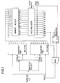
- a digital FSK transmitter illustrated in Figure 1 comprises a thirteen stage accumulator, a thirteen stage binary adder, and means for adding a number to the accumulator at a 3 MHz rate as determined by the CLOCK used for the accumulator, the adding means being constituted by two registers (register one and register two) and a register select circuit.
- the half period of the frequency generated must be a multiple of 333+ n seconds (the period is the reciprocal of the frequency).
- the best that can be done in generating these desired frequencies is to divide the 3 MHz generated by the clock by the divisors 158 and 98, giving 18.987 KHz and 30.612 KHz respectively.
- the accumulator maximum value should be divisible by both 158 and 198. The largest number, less than 8192, which is divisible by both 158 and 98 is 7742. This number is 450 short of the full accumulation value of 8192.
- a DATA IN signal to the register select circuit is binary in nature (0, 1) and corresponds to the frequency desired from the output FSK OUT of the accumulator.
- the register select circuit thus enables only the register one for an input signal of "1” and enables only the register two for an input signal of "0".
- the enabled register is thus activated to pass either of the two numbers stored therein to the binary adder.
- the register one has the numbers 49 and 274 stored therein while the register two has the numbers 79 and 304 stored therein.
- the enabled register will transmit either the higher or lower of the two numbers depending on whether it receives a HI or LO signal on a HI/LO input line.
- the HI/LO signal is derived from the output of an AND gate having inputs derived from the output of the 12th stage of the accumulator and an output Q ⁇ of a single stage shift register which has an input D from the 12th stage of the accumulator and is clocked by the 3 MHz CLOCK.
- the output Q of the shift register is the accumulator 12th stage delayed by one clock cycle of the 3 MHz clock input CLK.
- the LO numbers transmitted from the registers are due to the inputs to the AND gate being opposite in sign except when the 12th stage of the accumulator changes from a "0" to a "1" indicating the need for adding the previously-mentioned number 225 which is then added to the next normally transmitted number, either 49 or 79, to make for a single transmission of either 274 or 304 from the 13th stage of the accumulator depending on whether the register one or the register two of the accumulator is enabled.
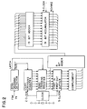
- Figure 2 illustrates a digital FSK receiver embodying the present invention. It has been designed so as to use much of the circuitry in the FSK transmitter shown in Figure 1.
- intervals between zero crossings are converted to numbers by counting the pulses of a clock, labelled ZCLOCK, in a (zero crossing) counter. At each zero crossing, the count resulting from the previous interval is stored in a (zero crossing) register.
- the value of the register is inserted in a 16 deep, 8 bit wide FIFO (first in-first out) buffer.
- An accumulator stores the sum of the values in the FIFO (plus a fixed offset). Rather than sum the 16 values each time, the accumulator is kept current by subtracting the oldest value in the FIFO from the new value being inserted and adding the resultant to the accumulator.
- the received signal FSK IN were a continuous "zero” (30.5 KHz), it would have zero crossing intervals of 16.393 microseconds. A continuous "one” (19 KHz) would have zero crossing intervals of 26.316 microseconds. With a ZCLOCK of 6 MHz, these intervals would yield counts of 98 and 158 respectively. Thus a continuous "0" input would give a value for the sum of the FIFO of 1568 and a continuous "1" input would give a value of 2528. The mid-point is 2048, or 2**11th. As seen in Figure 2, the baseband output RCVNR2 is the 12th stage of the accumulator (a "one" in the 12th stage has a value of 2**11th).
- the SCLOCK is 250 MHz and, because the 13 bit adder is relatively slow, it is not practical to subtract the old value of the buffer between successive SCLOCKs. Instead, an 8 bit adder calculates the difference between the new and the old values of the FIFO and this result is added to the accumulator at the SCLOCK rate. It is important to note that the result to be added to the accumulator may be positive or negative. A negative number from the 8 bit adder is automatically expressed in two's complement form, and so adding it to the accumulator will give the correct result.
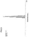
- the receiver embodying the present invention has been simulated using several BASIC programs. Calculations were performed to determine the spacings of zero crossings which would result from a perfect FSK transmitter being modulated by an input data stream. Delays were investigated for "one" to “zero” transitions and for "zero” to “one” transitions and the phase of the input data stream to the FSK signal was varied over all the possible values in increments of one microsecond.
- a third program was run to simulate the response of the circuit to a random input.
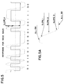
- the plot of the accumulator value compared to the input waveform is shown in Figure 5.
- the solid line waveform is the data input to an FSK transmitter.
- the "ones” and “zeroes” below the waveform show the data to be transmitted to a distant receiver.
- the dotted line waveform is the value in the accumulator of the distant receiver. As can be seen in Figure 5, the dotted line waveform has a number of changes in slope which will be described in more detail below.
- the upper flat portions of the dotted line waveform indicate that the FIFO contains 16 values of 158.
- the lower flat portions of the dotted line waveform indicate that the FIFO contains 16 values of 98.
- the slopes which connect the upper and lower portions are a function of when the change from a "one" to a "zero” or a "zero" to a "one” has occurred. If the data transition occurs at a zero crossing there will be a single slope. If the transition occurs between zero crossings, an intermediate count will be stored in the FIFO and three different slopes will occur as shown at slopes A, which are at a transition between a received "one” and a received "zero", in the dotted line waveform. An enlargement of the slopes A is shown in Figure 5A.
- a slope 1 of A occurs because 158 is being shifted out of the FIFO but a value less than 158 (and greater than 98) is being shifted in.
- a slope 2 occurs because 98 is being shifted into the FIFO and 158 is being shifted out.
- a slope 3 occurs when the intermediate values are shifted out of the FIFO and 98 is being shifted in.
- Figure 7 shows the actual results achieved in a gate array chip constructed according to the present technique.
- Figure 7 illustrates the delay between a transmitted signal CH1 and a received signal CH2.
Abstract
Description
- This invention relates to transmitting and receiving frequency-shift keyed (FSK) signals, and in particular to digital FSK transmitters, receivers and methods of recovering baseband signals from FSK signals.
- Frequency-shift keying is a form of frequency modulation used especially in telegraphic and facsimile transmission. The modulating wave in frequency-shift keying shifts the output frequency between predetermined values corresponding to the frequencies of correlated sources.
- Digital FSK transmitters are known. A digital phase locked loop (PLL) which can be used as a component of an FSK receiver is also known, but this circuit requires the use of an analog filter to operate as an FSK receiver. Also, in order to implement a digital FSK receiver according to known techniques, it is necessary to use a mixed-mode ASIC (application specific integrated circuit) which is both expensive and requires a comparatively long development time.
- According to one aspect of the invention there is provided a digital FSK receiver for receiving an FSK signal containing at least two different signal frequencies, the receiver comprising:
a zero crossing detector for detecting zero crossings of the FSK signal;
interval measuring means connected to the zero crossing detector for measuring the intervals between the zero crossings, the intervals having a first value when the FSK signal is at one of the signal frequencies, a second value when the FSK signal is at another of the signal frequencies, and a plurality of intermediate values which are between the first and second values when the FSK signal switches between the frequencies; and
binary output means connected to the interval measuring means for receiving the interval values and for outputting a binary signal which switches between logical zero and logical one states when the binary output means receives one of the intermediate values. - According to another aspect of the invention there is provided a method of recovering a baseband signal from an FSK signal having at least two different signal frequencies, the method comprising:
detecting the zero crossings in the FSK signal;
measuring the intervals between the zero crossings of the FSK signal, the intervals having a first value when the FSK signal is at one of the signal frequencies, a second value when the FSK signal is at another of the signal frequencies and a plurality of intermediate values which are between the first and second values when the FSK signal switches between the frequencies; and
generating a binary signal which switches between logical zero and logical one states when the interval is at one of the intermediate values. - According to a further aspect of the invention there is provided an FSK transmitter for transmitting an FSK signal containing at least two different signal frequencies; the transmitter comprising:
an accumulator having a set number of stages;
an adder connected to said accumulator for adding numbers thereto;
means for adding a selected one of a pair of numbers from said adder to said accumulator at a set frequency rate;
a clock driving said accumulator at a set frequency to output a first and second frequency output signal; and
means for feeding back said clock signal to said adding means selectively to pass said one of said pair of numbers therefrom to said adder. - A preferred embodiment of this invention provides a digital FSK transmitter receiver which utilises information contained in the zero crossings of the received FSK signal. The FSK signal is transmitted by a dual register preprogrammed to add a predetermined count to an accumulator through an adder to generate the exact dual FSK frequencies required. The same clock signal used for the accumulator is also used as a signal for the dual registers by way of the signal going to a single stage shift register.
- The zero crossings of the transmitted FSK signals are converted to a digital format by counting the number of clock pulses between successive zero crossings. A second clock is used to insert the last zero crossing count into a multistage first in-first out (FIFO) buffer. An accumulator stores the sum of the values in the FIFO. A threshold is established whereby any value in the accumulator below the threshold is considered a zero and any value above is considered a one.
- The accumulator and the FIFO serve as a "digital" filter. If a zero crossing is received early (or late) as a result of noise, the value in the accumulator will decrease (or increase). However, if the next zero crossing is not displaced, it will bring the accumulator back to its expected value.
- Extensive computer simulations have demonstrated the utility of this arrangement.
- The preferred digital FSK transmitter receiver has several advantages over known analog FSK receivers. The digital FSK receiver allows the use of a gate array rather than a mixed-mode ASIC. A gate array implementation is cheaper to develop, requires less turn-around time, and reduces the part per price to less than half that of a mixed-mode ASIC. The digital FSK receiver also does not require a filter which is necessary in analog FSK receivers. This can reduce the board area required for the equipment by up to a factor of two. Where it is required to provide both a transmitter and a receiver, the two circuits can share a number of components, including an adder and an accumulator.
- The present invention further provides a digital FSK receiver for receiving an FSK signal containing at least two different signal frequencies, the receiver comprising: a zero crossing detector for detecting zero crossings of the FSK signal; interval measuring means connected to the zero crossing detector for measuring the intervals between the zero crossings; a buffer for storing a number of previous zero crossing values; an accumulator for maintaining the sum of the stored zero crossing values (with a possible fixed offset); and a binary output means for outputting a one or a zero depending on whether the value in the accumulator is above or below a selected threshold.
- The invention will now be described by way of example with reference to the accompanying drawings, throughout which like parts are referred to by like references, and in which:
- Figure 1 is a block diagram showing a digital FSK transmitter which can be used to generate a binary FSK signal;
- Figure 2 is a block diagram of a digital FSK receiver according to an embodiment of the present invention;
- Figure 3 is a graph plotting a signal against time and illustrating a delay distribution resulting from one simulation of the present technique;
- Figure 4 is a view similar to Figure 3 illustrating a delay distribution of a different simulation of the technique;
- Figure 5 illustrates a waveform showing the correlation between a signal fed into an FSK transmitter and the corresponding value in an accumulator of an FSK receiver which is receiving the output of the above transmission;
- Figure 5A is a section of the waveform shown in Figure 5, with an expanded time scale to illustrate better the different slopes of the waveform;
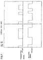
- Figure 6 is a view similar to Figure 5 with the FSK transmitter input artificially delayed to illustrate better the correlation between the waveforms; and
- Figure 7 graphically illustrates the transmitted and received FSK signals for two operating chips embodying the present invention.
- A digital FSK transmitter illustrated in Figure 1 comprises a thirteen stage accumulator, a thirteen stage binary adder, and means for adding a number to the accumulator at a 3 MHz rate as determined by the CLOCK used for the accumulator, the adding means being constituted by two registers (register one and register two) and a register select circuit. With a fixed number N, the thirteenth stage of the accumulator would alternate between a "one" and a "zero" with an average frequency at the output FSK OUT determined by the formula:

where: - freq (N) ave
- = average FSK frequency
- 3,000,000
- =
CLOCK frequency 3 MHz - N
- = number added to the accumulator
- 8192
- = 2¹³ as determined by the 13 stages of the accumulator, each stage having 2 values.
- This is specified as an average frequency because, if N is not a factor of 8192 (2**13th - 8192), the frequency generated will shift between two frequencies such that the average is that defined above. In FSK transmission, the actual frequency is important rather than the average.
- In one example, it is desired to generate FSK frequencies of 19 KHz and 30.5 KHz. With a 3 MHz clock, the half period of the frequency generated must be a multiple of 333+ n seconds (the period is the reciprocal of the frequency). The best that can be done in generating these desired frequencies is to divide the 3 MHz generated by the clock by the
divisors - In operation, a DATA IN signal to the register select circuit is binary in nature (0, 1) and corresponds to the frequency desired from the output FSK OUT of the accumulator. The register select circuit thus enables only the register one for an input signal of "1" and enables only the register two for an input signal of "0". The enabled register is thus activated to pass either of the two numbers stored therein to the binary adder. The register one has the numbers 49 and 274 stored therein while the register two has the numbers 79 and 304 stored therein. The enabled register will transmit either the higher or lower of the two numbers depending on whether it receives a HI or LO signal on a HI/LO input line.
- The HI/LO signal is derived from the output of an AND gate having inputs derived from the output of the 12th stage of the accumulator and an output

- Thus the AND gate will generate a LO signal for all but one clock cycle of each half cycle of the output FSK OUT. Since it is required to divide the 3 MHz clock by 158 or 98, depending on the data input, if there is an input of "one", 49 will be added 156 times and 274 twice for each cycle of FSK OUT, and 49*156 + 2*274 = 8192. If there is an input of "zero", 79 will be added 96 times and 304 twice, and 79*96 + 2*304 = 8192.
- The LO numbers transmitted from the registers are due to the inputs to the AND gate being opposite in sign except when the 12th stage of the accumulator changes from a "0" to a "1" indicating the need for adding the previously-mentioned number 225 which is then added to the next normally transmitted number, either 49 or 79, to make for a single transmission of either 274 or 304 from the 13th stage of the accumulator depending on whether the register one or the register two of the accumulator is enabled.
- Figure 2 illustrates a digital FSK receiver embodying the present invention. It has been designed so as to use much of the circuitry in the FSK transmitter shown in Figure 1. In Figure 2, intervals between zero crossings are converted to numbers by counting the pulses of a clock, labelled ZCLOCK, in a (zero crossing) counter. At each zero crossing, the count resulting from the previous interval is stored in a (zero crossing) register. On each pulse of another clock SCLOCK, the value of the register is inserted in a 16 deep, 8 bit wide FIFO (first in-first out) buffer. An accumulator stores the sum of the values in the FIFO (plus a fixed offset). Rather than sum the 16 values each time, the accumulator is kept current by subtracting the oldest value in the FIFO from the new value being inserted and adding the resultant to the accumulator.
- If the received signal FSK IN were a continuous "zero" (30.5 KHz), it would have zero crossing intervals of 16.393 microseconds. A continuous "one" (19 KHz) would have zero crossing intervals of 26.316 microseconds. With a ZCLOCK of 6 MHz, these intervals would yield counts of 98 and 158 respectively. Thus a continuous "0" input would give a value for the sum of the FIFO of 1568 and a continuous "1" input would give a value of 2528. The mid-point is 2048, or 2**11th. As seen in Figure 2, the baseband output RCVNR2 is the 12th stage of the accumulator (a "one" in the 12th stage has a value of 2**11th).
- When the transmitted data changes from "1" to "0" (or "0" to "1") there will be one zero crossing interval which will be between the two extremes. This intermediate count contains information which allows the receiver to determine where within the interval the change occurred. It is imperative for minimum jitter reception that this intermediate value be retained.
- In the present embodiment, the SCLOCK is 250 MHz and, because the 13 bit adder is relatively slow, it is not practical to subtract the old value of the buffer between successive SCLOCKs. Instead, an 8 bit adder calculates the difference between the new and the old values of the FIFO and this result is added to the accumulator at the SCLOCK rate. It is important to note that the result to be added to the accumulator may be positive or negative. A negative number from the 8 bit adder is automatically expressed in two's complement form, and so adding it to the accumulator will give the correct result.
- The receiver embodying the present invention has been simulated using several BASIC programs. Calculations were performed to determine the spacings of zero crossings which would result from a perfect FSK transmitter being modulated by an input data stream. Delays were investigated for "one" to "zero" transitions and for "zero" to "one" transitions and the phase of the input data stream to the FSK signal was varied over all the possible values in increments of one microsecond.
- In the first program, the delay in the change of the output relative to a change in the input data stream from a "one" to a "zero" was investigated. The time t = 0 was arbitrarily set to the last zero crossing before the input data changed. The program was run a number of times for the input changing at t = 1 microseconds, 2 microseconds, up to 26 microseconds. The limit is 26 microseconds because, if it were any later than that, another zero crossing would occur before the input change. Figure 3 shows the distribution of the delays (time of output change minus time of input change). The actual values are given in Table 1, and the program is listed in Table 2.
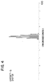
- Similarly, the delay due to a change from a "zero" to a "one" was investigated. The distribution is shown in Figure 4, the values are listed in Table 3, and the program is given in Table 4.
- When the programs were originally run, the distribution for both cases was about +/- 3.5%, but the average delays were different. This would result in a bias, causing "ones" and "zeros" not to have the same duration. The simplest way to counteract this bias is to offset the value stored in the accumulator, such that: Accumulator Value = Sum of FIFO + NCOR where NCOR is a positive or negative correction integer.
- A third program was run to simulate the response of the circuit to a random input. The plot of the accumulator value compared to the input waveform is shown in Figure 5.
- In Figure 5, the solid line waveform is the data input to an FSK transmitter. The "ones" and "zeroes" below the waveform show the data to be transmitted to a distant receiver. The dotted line waveform is the value in the accumulator of the distant receiver. As can be seen in Figure 5, the dotted line waveform has a number of changes in slope which will be described in more detail below.
- The upper flat portions of the dotted line waveform indicate that the FIFO contains 16 values of 158. The lower flat portions of the dotted line waveform indicate that the FIFO contains 16 values of 98. The slopes which connect the upper and lower portions are a function of when the change from a "one" to a "zero" or a "zero" to a "one" has occurred. If the data transition occurs at a zero crossing there will be a single slope. If the transition occurs between zero crossings, an intermediate count will be stored in the FIFO and three different slopes will occur as shown at slopes A, which are at a transition between a received "one" and a received "zero", in the dotted line waveform. An enlargement of the slopes A is shown in Figure 5A.
- Just prior to the first slope in A, a "one" is being received and 158 is being shifted in and out of the FIFO. A
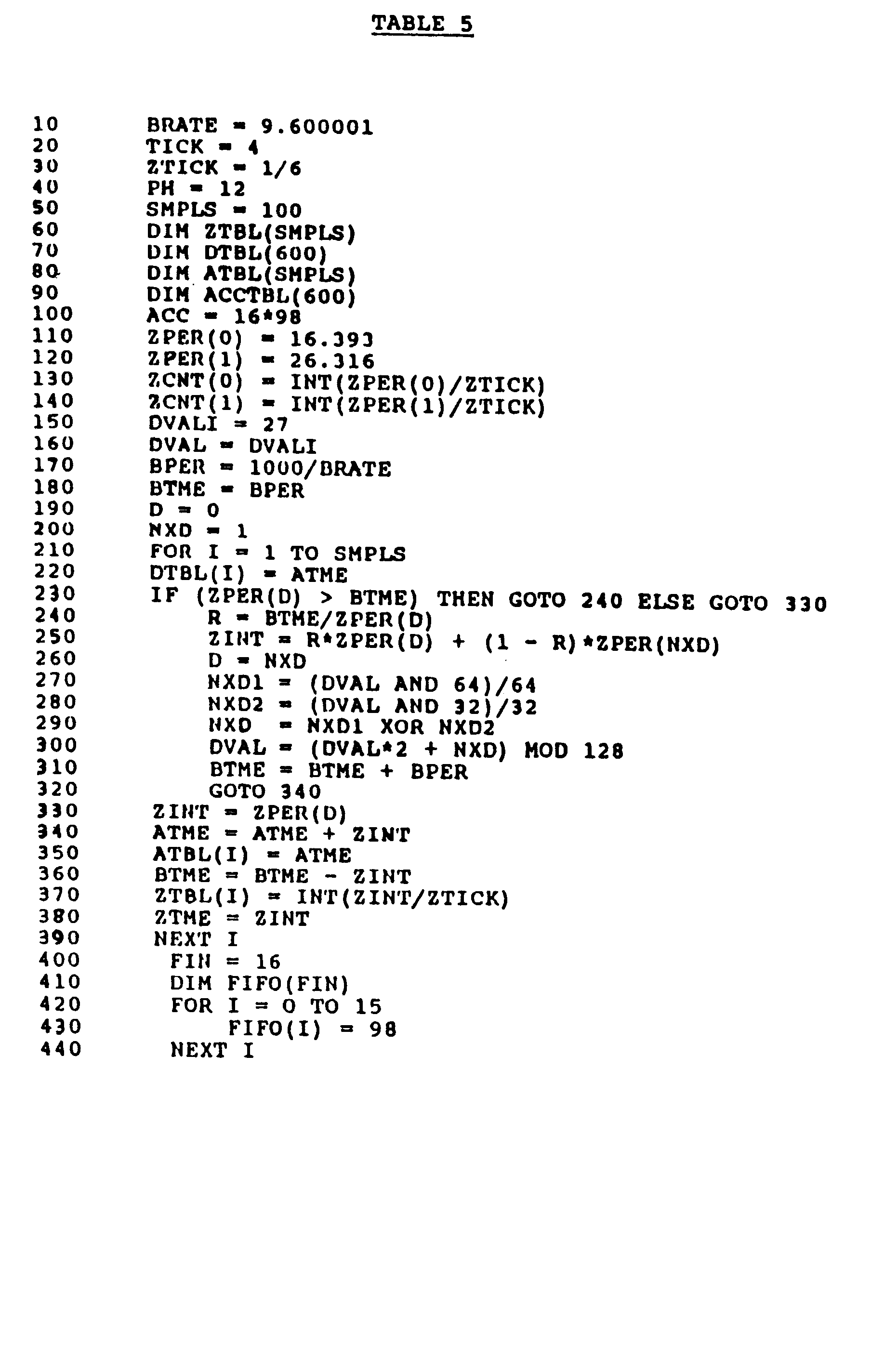
slope 1 of A occurs because 158 is being shifted out of the FIFO but a value less than 158 (and greater than 98) is being shifted in. Aslope 2 occurs because 98 is being shifted into the FIFO and 158 is being shifted out. Aslope 3 occurs when the intermediate values are shifted out of the FIFO and 98 is being shifted in. When all of the intermediate values are shifted out of the FIFO, the FIFO is loaded with all 98s and the waveform is at the lower flat portion. So as to make it easier to compare the two waveforms, they are shown in Figure 6 with input delayed. In both plots, the dotted line is set at the count 2048. The program is listed in Table 5. - A basic design for an all-digital FSK circuit has been disclosed which, without any enhancements, is likely to satisfy all basic requirements.
- Figure 7 shows the actual results achieved in a gate array chip constructed according to the present technique. Figure 7 illustrates the delay between a transmitted signal CH1 and a received signal CH2.


Claims (15)
- A digital FSK receiver for receiving an FSK signal (FSK IN) containing at least two different signal frequencies, the receiver comprising:
a zero crossing detector for detecting zero crossings of the FSK signal;
interval measuring means connected to the zero crossing detector for measuring the intervals between the zero crossings, the intervals having a first value when the FSK signal is at one of the signal frequencies, a second value when the FSK signal is at another of the signal frequencies, and a plurality of intermediate values which are between the first and second values when the FSK signal switches between the frequencies; and
binary output means connected to the interval measuring means for receiving the interval values and for outputting a binary signal (RCVNR2) which switches between logical zero and logical one states when the binary output means receives one of the intermediate values. - A digital FSK receiver according to claim 1, wherein the interval measuring means comprises a zero crossing counter connected to the zero crossing detector, a clock connected to the zero crossing counter for pulsing the zero crossing counter a plurality of times between each zero crossing, the zero crossing counter being operable to count the number of clock pulses between intervals, and a zero crossing register connected to the zero crossing counter for storing the number of clock pulses counted during each interval which corresponds to one of the values for the interval.
- A digital FSK receiver according to claim 2, wherein the interval measuring means includes a first in-first out buffer for receiving the contents of the zero crossing register and for applying the contents of the zero crossing register to the binary output means.
- A digital FSK receiver according to claim 3, wherein the binary output means comprises an accumulator having an input, an output for the binary zeros and ones, and a first binary adder connected between the buffer and the accumulator input for accumulating the interval values in the accumulator.
- A digital FSK receiver according to claim 4, wherein the first in-first out buffer is connected to the zero crossing register, and including a complementor connected to an output of the first in-first out buffer and a second binary adder having a first input connected to the output of the zero crossing register and a second input connected to the output of the complementor, the second binary adder having an output connected to an input of the first binary adder.
- A method of recovering a baseband signal from an FSK signal (FSK IN) having at least two different signal frequencies, the method comprising:
detecting the zero crossings in the FSK signal;
measuring the intervals between the zero crossings of the FSK signal, the intervals having a first value when the FSK signal is at one of the signal frequencies, a second value when the FSK signal is at another of the signal frequencies and a plurality of intermediate values which are between the first and second values when the FSK signal switches between the frequencies; and
generating a binary signal (RCVNR2) which switches between logical zero and logical one states when the interval is at one of the intermediate values. - A method according to claim 6, including measuring the intervals between zero crossings by counting clock pulses between zero crossings and storing the counted clock pulses in a register.
- A method according to claim 7, including applying the stored counted pulses to a first in-first out buffer and outputting a signal from the first in-first out buffer to a binary adder and means for converting the counted pulses to the logical zeros and ones.
- A method according to claim 8, wherein the converting means is operable to accumulate the interval values from the adder and to output the binary signal based on the accumulated interval values.
- An FSK transmitter for transmitting an FSK signal (FSK OUT) containing at least two different signal frequencies; the transmitter comprising:
an accumulator having a set number of stages;
an adder connected to said accumulator for adding numbers thereto;
means for adding a selected one of a pair of numbers from said adder to said accumulator at a set frequency rate;
a clock driving said accumulator at a set frequency to output a first and second frequency output signal; and
means for feeding back said clock signal to said adding means selectively to pass said one of said pair of numbers therefrom to said adder. - An FSK transmitter according to claim 10, wherein the adding means includes at least two registers having a pair of numbers stored therein and being responsive to an enable signal along with a binary HI/LO signal to transmit one or the other of said pair of numbers depending on the condition of the binary HI/LO signal.
- An FSK transmitter according to claim 11, wherein the two registers have a different pair of numbers stored therein, each being responsive to the enable signal and the HI/LO signal to transmit one of the pair of numbers to said accumulator.
- An FSK transmitter according to claim 10, claim 11 or claim 12, wherein said feedback means provides a HI/LO signal derived from a combination of an accumulator output signal and said clock frequency signal modified through a shift register stage.
- An FSK transmitter according to claim 13, wherein said shift register stage has a first input from said accumulator and a second input from said clock of said accumulator, and provides a signal which is the opposite of the accumulator input delayed by one clock cycle.
- An FSK transmitter according to claim 14, wherein said HI/LO signal is derived from an AND gate having one input from said accumulator and a second input from said shift register stage.
Priority Applications (1)
| Application Number | Priority Date | Filing Date | Title |
|---|---|---|---|
| EP00115544A EP1051004A3 (en) | 1991-08-30 | 1992-08-24 | Receiver and method for receiving FSK signals |
Applications Claiming Priority (2)
| Application Number | Priority Date | Filing Date | Title |
|---|---|---|---|
| US752758 | 1991-08-30 | ||
| US07/752,758 US5311556A (en) | 1991-08-30 | 1991-08-30 | Digital FSK transmitter receiver and method of operating same |
Related Child Applications (1)
| Application Number | Title | Priority Date | Filing Date |
|---|---|---|---|
| EP00115544A Division EP1051004A3 (en) | 1991-08-30 | 1992-08-24 | Receiver and method for receiving FSK signals |
Publications (2)
| Publication Number | Publication Date |
|---|---|
| EP0529986A2 true EP0529986A2 (en) | 1993-03-03 |
| EP0529986A3 EP0529986A3 (en) | 1993-09-29 |
Family
ID=25027711
Family Applications (2)
| Application Number | Title | Priority Date | Filing Date |
|---|---|---|---|
| EP00115544A Withdrawn EP1051004A3 (en) | 1991-08-30 | 1992-08-24 | Receiver and method for receiving FSK signals |
| EP19920307693 Ceased EP0529986A3 (en) | 1991-08-30 | 1992-08-24 | Fsk modulator and demodulator |
Family Applications Before (1)
| Application Number | Title | Priority Date | Filing Date |
|---|---|---|---|
| EP00115544A Withdrawn EP1051004A3 (en) | 1991-08-30 | 1992-08-24 | Receiver and method for receiving FSK signals |
Country Status (7)
| Country | Link |
|---|---|
| US (2) | US5311556A (en) |
| EP (2) | EP1051004A3 (en) |
| JP (1) | JPH05284181A (en) |
| AU (2) | AU653053B2 (en) |
| BR (1) | BR9203324A (en) |
| CA (1) | CA2077227C (en) |
| MX (1) | MX9204989A (en) |
Cited By (7)
| Publication number | Priority date | Publication date | Assignee | Title |
|---|---|---|---|---|
| GB2286951A (en) * | 1994-02-21 | 1995-08-30 | Mitel Corp | Digital FSK receiver using double zero-crossing detection |
| EP0991234A1 (en) * | 1998-10-02 | 2000-04-05 | Faure Research SARL | Digital FSK demodulator |
| FR2811170A1 (en) * | 2000-07-03 | 2002-01-04 | Valeo Electronique | ANTENNA PILOT TRANSMITTING A SYNCHRONIZED FREQUENCY SWITCHED BI-FREQUENCY SIGNAL |
| EP1225738A1 (en) * | 2001-01-23 | 2002-07-24 | Sagem S.A. | Adaptive bidirectional modem with filtering means common to the emission and the reception blocks and arranged to operate alternately |
| WO2003084052A1 (en) * | 2002-04-02 | 2003-10-09 | Infineon Technologies Ag | Demodulation of a digitally frequency modulated analogue received signal by evaluation of the time difference between the null transitions |
| WO2005027452A1 (en) * | 2003-09-12 | 2005-03-24 | Infineon Technologies Ag | Method for the reconstruction of zero crossing information of noisy angle-modulated signals following limiter-discriminator signal processing |
| EP2225862A4 (en) * | 2007-12-28 | 2015-12-16 | Spectrum Controls Inc | Micro-controller with fsk modem |
Families Citing this family (16)
| Publication number | Priority date | Publication date | Assignee | Title |
|---|---|---|---|---|
| US5513219A (en) * | 1994-08-26 | 1996-04-30 | Compaq Computer Corporation | Apparatus and method for transmitting information with a subminimally modulated transmission signal |
| FR2738423B1 (en) * | 1995-08-30 | 1997-09-26 | Snecma | DIGITAL FREQUENCY DEMODULATOR |
| US5712878A (en) * | 1996-08-19 | 1998-01-27 | Elsag International N.V. | Digital FSK modulator |
| KR100186753B1 (en) * | 1996-08-24 | 1999-05-15 | 삼성전자주식회사 | Radio transmit and receive system |
| US6144253A (en) * | 1997-10-27 | 2000-11-07 | Elsag International N.V. | Digital FSK demodulator |
| US6272184B1 (en) * | 1997-12-17 | 2001-08-07 | Conexant Systems, Inc. | Non-coherent frequency shift keying detection scheme |
| US6990157B2 (en) * | 2001-02-24 | 2006-01-24 | Texas Instruments Incorporated | All-digital FSK demodulation with selectable data rate and adjustable resolution |
| US7003049B2 (en) * | 2001-06-12 | 2006-02-21 | Rf Micro Devices, Inc. | Fractional-N digital modulation with analog IQ interface |
| US6448831B1 (en) | 2001-06-12 | 2002-09-10 | Rf Micro Devices, Inc. | True single-phase flip-flop |
| US6693468B2 (en) | 2001-06-12 | 2004-02-17 | Rf Micro Devices, Inc. | Fractional-N synthesizer with improved noise performance |
| US6385276B1 (en) | 2001-06-12 | 2002-05-07 | Rf Micro Devices, Inc. | Dual-modulus prescaler |
| US6779010B2 (en) | 2001-06-12 | 2004-08-17 | Rf Micro Devices, Inc. | Accumulator with programmable full-scale range |
| US6891905B1 (en) * | 2001-08-23 | 2005-05-10 | National Semiconductor Corporation | Apparatus and method for FSK demodulation with integrated time and frequency tracking |
| US7292637B2 (en) * | 2003-12-17 | 2007-11-06 | Rambus Inc. | Noise-tolerant signaling schemes supporting simplified timing and data recovery |
| US8373357B2 (en) * | 2009-01-26 | 2013-02-12 | Microchip Technology Incorporated | Modulator module in an integrated circuit device |
| IT201600111351A1 (en) * | 2016-11-04 | 2018-05-04 | St Microelectronics Des & Appl | PROCEDURE FOR REVEALING SIGNALS WITH FSK MODULATION, CIRCUIT, DEVICE AND CORRESPONDENT COMPUTER PRODUCT |
Citations (2)
| Publication number | Priority date | Publication date | Assignee | Title |
|---|---|---|---|---|
| US4021744A (en) * | 1975-03-18 | 1977-05-03 | Societa Italiana Telecomunicazioni Siemens S.P.A. | Demodulator for frequency-keyed communication system |
| GB2102223A (en) * | 1981-05-08 | 1983-01-26 | Suwa Seikosha Kk | A frequency shift keying demodulation circuit |
Family Cites Families (11)
| Publication number | Priority date | Publication date | Assignee | Title |
|---|---|---|---|---|
| US3597599A (en) * | 1969-06-16 | 1971-08-03 | Collins Radio Co | Digitalized tone generator |
| US3937932A (en) * | 1974-04-15 | 1976-02-10 | Barber-Colman Company | Digital frequency generator |
| GB1506579A (en) * | 1974-10-17 | 1978-04-05 | Ching Koon Pun | Leak-resistant dry cells |
| JPS5310253A (en) * | 1976-07-16 | 1978-01-30 | Sharp Corp | Fs signal demodulator |
| US4349887A (en) * | 1980-08-22 | 1982-09-14 | Rca Corporation | Precise digitally programmed frequency source |
| US4485347A (en) * | 1980-09-04 | 1984-11-27 | Mitsubishi Denki Kabushiki Kaisha | Digital FSK demodulator |
| US4627078A (en) * | 1983-08-25 | 1986-12-02 | The Microperipheral Corporation | Data communication system |
| US4757519A (en) * | 1987-10-02 | 1988-07-12 | Hewlett-Packard | Digital premodulation filter |
| US4785255A (en) * | 1987-11-23 | 1988-11-15 | Allen-Bradley Company, Inc. | Digital FSK signal demodulator |
| US5105444A (en) * | 1989-09-13 | 1992-04-14 | Atlantic Richfield Company | System for high speed data tranmission |
| DE3939259A1 (en) * | 1989-11-28 | 1991-05-29 | Rohde & Schwarz | FREQUENCY MODULABLE FREQUENCY GENERATOR |
-
1991
- 1991-08-30 US US07/752,758 patent/US5311556A/en not_active Expired - Fee Related
-
1992
- 1992-08-24 EP EP00115544A patent/EP1051004A3/en not_active Withdrawn
- 1992-08-24 EP EP19920307693 patent/EP0529986A3/en not_active Ceased
- 1992-08-26 BR BR929203324A patent/BR9203324A/en not_active Application Discontinuation
- 1992-08-28 MX MX9204989A patent/MX9204989A/en not_active IP Right Cessation
- 1992-08-28 AU AU21399/92A patent/AU653053B2/en not_active Ceased
- 1992-08-31 JP JP4253556A patent/JPH05284181A/en not_active Withdrawn
- 1992-08-31 CA CA002077227A patent/CA2077227C/en not_active Expired - Fee Related
-
1993
- 1993-03-17 US US08/032,938 patent/US5365548A/en not_active Expired - Fee Related
-
1994
- 1994-08-12 AU AU70257/94A patent/AU669815B2/en not_active Ceased
Patent Citations (2)
| Publication number | Priority date | Publication date | Assignee | Title |
|---|---|---|---|---|
| US4021744A (en) * | 1975-03-18 | 1977-05-03 | Societa Italiana Telecomunicazioni Siemens S.P.A. | Demodulator for frequency-keyed communication system |
| GB2102223A (en) * | 1981-05-08 | 1983-01-26 | Suwa Seikosha Kk | A frequency shift keying demodulation circuit |
Cited By (14)
| Publication number | Priority date | Publication date | Assignee | Title |
|---|---|---|---|---|
| GB2286951A (en) * | 1994-02-21 | 1995-08-30 | Mitel Corp | Digital FSK receiver using double zero-crossing detection |
| US5661759A (en) * | 1994-02-21 | 1997-08-26 | Mitel Corporation | Digital FSK receiver using double zero-crossing |
| GB2286951B (en) * | 1994-02-21 | 1998-04-15 | Mitel Corp | Digital fsk receiver using double zero-crossing |
| EP0991234A1 (en) * | 1998-10-02 | 2000-04-05 | Faure Research SARL | Digital FSK demodulator |
| FR2784256A1 (en) * | 1998-10-02 | 2000-04-07 | Faure Research | DIGITAL DEMODULATOR, AND METHOD FOR DEMODULATING A MODULATED SIGNAL BY FREQUENCY DISPLACEMENT |
| EP1170873A1 (en) * | 2000-07-03 | 2002-01-09 | Valeo Electronique | Phase coherent FSK transmitter |
| FR2811170A1 (en) * | 2000-07-03 | 2002-01-04 | Valeo Electronique | ANTENNA PILOT TRANSMITTING A SYNCHRONIZED FREQUENCY SWITCHED BI-FREQUENCY SIGNAL |
| EP1225738A1 (en) * | 2001-01-23 | 2002-07-24 | Sagem S.A. | Adaptive bidirectional modem with filtering means common to the emission and the reception blocks and arranged to operate alternately |
| FR2819970A1 (en) * | 2001-01-23 | 2002-07-26 | Sagem | METHOD FOR SETTING UP AND USING A BIDIRECTIONAL DATA LINK AND MODEM FOR IMPLEMENTING THE METHOD |
| WO2003084052A1 (en) * | 2002-04-02 | 2003-10-09 | Infineon Technologies Ag | Demodulation of a digitally frequency modulated analogue received signal by evaluation of the time difference between the null transitions |
| US7646827B2 (en) | 2002-04-02 | 2010-01-12 | Infineon Technologies Ag | Demodulation of a digitally frequency-modulated analog received signal by evaluation of the time intervals between the zero crossings |
| CN1647363B (en) * | 2002-04-02 | 2010-12-01 | 因芬尼昂技术股份公司 | Method for reception, processing and demodulation of a digitally frequency modulated analogue signal in communication system |
| WO2005027452A1 (en) * | 2003-09-12 | 2005-03-24 | Infineon Technologies Ag | Method for the reconstruction of zero crossing information of noisy angle-modulated signals following limiter-discriminator signal processing |
| EP2225862A4 (en) * | 2007-12-28 | 2015-12-16 | Spectrum Controls Inc | Micro-controller with fsk modem |
Also Published As
| Publication number | Publication date |
|---|---|
| AU669815B2 (en) | 1996-06-20 |
| EP1051004A2 (en) | 2000-11-08 |
| CA2077227A1 (en) | 1993-03-01 |
| EP0529986A3 (en) | 1993-09-29 |
| AU7025794A (en) | 1994-10-13 |
| AU2139992A (en) | 1993-03-04 |
| US5311556A (en) | 1994-05-10 |
| MX9204989A (en) | 1993-04-01 |
| US5365548A (en) | 1994-11-15 |
| BR9203324A (en) | 1993-04-06 |
| CA2077227C (en) | 1998-09-15 |
| AU653053B2 (en) | 1994-09-15 |
| JPH05284181A (en) | 1993-10-29 |
| EP1051004A3 (en) | 2001-01-10 |
Similar Documents
| Publication | Publication Date | Title |
|---|---|---|
| EP0529986A2 (en) | FSK modulator and demodulator | |
| EP0112043B1 (en) | Self-clocking binary receiver | |
| US4346477A (en) | Phase locked sampling radio receiver | |
| EP0469233A2 (en) | Digital synthesizer with phase memory | |
| EP0740423A3 (en) | Digital phase-locked loop | |
| US5365543A (en) | Transmitting circuit and receiving circuit | |
| KR880003494A (en) | Bit Synchronization Circuit and Its Method | |
| US20090098834A1 (en) | Frequency synthesizer, radio communication system, and semiconductor device | |
| US5754606A (en) | Clock signal regenerating circuit | |
| US5103185A (en) | Clock jitter suppressing circuit | |
| EP0459446B1 (en) | Numerical controlled oscillator | |
| US6137332A (en) | Clock signal generator and data signal generator | |
| CA1263455A (en) | Frequency multiplier circuit | |
| US7664166B2 (en) | Pleisiochronous repeater system and components thereof | |
| EP0809358A2 (en) | Method of transmitting clock signal and device employing the same | |
| US5850161A (en) | Digital FM demodulator using pulse generators | |
| JP3154302B2 (en) | Phase difference detection circuit | |
| JPH08154069A (en) | Receiver for spread spectrum communication | |
| US5311559A (en) | Apparatus for correcting waveform distortion | |
| KR100236084B1 (en) | Clock signal generator | |
| JPS6347389B2 (en) | ||
| JP3344530B2 (en) | Digital signal transmission method and digital signal demodulation device | |
| SU1100714A1 (en) | Digital filter for frequency-shift keyed signals with unknown phase | |
| JP3037209B2 (en) | Phase difference detection circuit | |
| KR950002305B1 (en) | Synchronous clock generating circuit by receiving data |
Legal Events
| Date | Code | Title | Description |
|---|---|---|---|
| PUAI | Public reference made under article 153(3) epc to a published international application that has entered the european phase |
Free format text: ORIGINAL CODE: 0009012 |
|
| AK | Designated contracting states |
Kind code of ref document: A2 Designated state(s): DE ES FR GB IT NL |
|
| PUAL | Search report despatched |
Free format text: ORIGINAL CODE: 0009013 |
|
| AK | Designated contracting states |
Kind code of ref document: A3 Designated state(s): DE ES FR GB IT NL |
|
| 17P | Request for examination filed |
Effective date: 19940214 |
|
| 17Q | First examination report despatched |
Effective date: 19990209 |
|
| RIC1 | Information provided on ipc code assigned before grant |
Free format text: 7H 04L 27/12 A |
|
| RTI1 | Title (correction) |
Free format text: FSK TRANSMITTER |
|
| GRAG | Despatch of communication of intention to grant |
Free format text: ORIGINAL CODE: EPIDOS AGRA |
|
| STAA | Information on the status of an ep patent application or granted ep patent |
Free format text: STATUS: THE APPLICATION HAS BEEN REFUSED |
|
| 18R | Application refused |
Effective date: 20010805 |