EP0528572B2 - Vorrichtung zur Verschlüsselung und Entschlüsselung von Signalen - Google Patents
Vorrichtung zur Verschlüsselung und Entschlüsselung von Signalen Download PDFInfo
- Publication number
- EP0528572B2 EP0528572B2 EP92307041A EP92307041A EP0528572B2 EP 0528572 B2 EP0528572 B2 EP 0528572B2 EP 92307041 A EP92307041 A EP 92307041A EP 92307041 A EP92307041 A EP 92307041A EP 0528572 B2 EP0528572 B2 EP 0528572B2
- Authority
- EP
- European Patent Office
- Prior art keywords
- coding device
- storage memory
- electronic coding
- configuration storage
- encryption
- Prior art date
- Legal status (The legal status is an assumption and is not a legal conclusion. Google has not performed a legal analysis and makes no representation as to the accuracy of the status listed.)
- Expired - Lifetime
Links
Images

Classifications
-
- G—PHYSICS
- G09—EDUCATION; CRYPTOGRAPHY; DISPLAY; ADVERTISING; SEALS
- G09C—CIPHERING OR DECIPHERING APPARATUS FOR CRYPTOGRAPHIC OR OTHER PURPOSES INVOLVING THE NEED FOR SECRECY
- G09C1/00—Apparatus or methods whereby a given sequence of signs, e.g. an intelligible text, is transformed into an unintelligible sequence of signs by transposing the signs or groups of signs or by replacing them by others according to a predetermined system
-
- G—PHYSICS
- G06—COMPUTING OR CALCULATING; COUNTING
- G06F—ELECTRIC DIGITAL DATA PROCESSING
- G06F21/00—Security arrangements for protecting computers, components thereof, programs or data against unauthorised activity
- G06F21/30—Authentication, i.e. establishing the identity or authorisation of security principals
- G06F21/44—Program or device authentication
-
- G—PHYSICS
- G06—COMPUTING OR CALCULATING; COUNTING
- G06F—ELECTRIC DIGITAL DATA PROCESSING
- G06F2221/00—Indexing scheme relating to security arrangements for protecting computers, components thereof, programs or data against unauthorised activity
- G06F2221/21—Indexing scheme relating to G06F21/00 and subgroups addressing additional information or applications relating to security arrangements for protecting computers, components thereof, programs or data against unauthorised activity
- G06F2221/2135—Metering
Definitions
- THIS INVENTION relates to an electronic device for encoding or decoding electrical signals.
- data in encrypted form is transmitted by a transmitter to a receiver.
- the received encrypted data is then decrypted, validated by a control unit, and then further processed according to the requirements of the application.
- the security of encrypted data transmission may be increased in various ways.
- the encryption key may be made to vary randomly and used only once. Such an encryption key is known as a "one time key”.
- the encryption key may be fixed and the data to be combined with the key may be varied. This method of data encryption is known in the art as "code hopping”.
- Japanese Patent Number 63-155930 discloses a method of providing encrypted data for secure transmission across a public data network.
- the method comprises generating an encryption key, and the transmission of the key from the transmitter to the receiver, or vice-versa, across the public data network.
- Network processors at the transmitter and receiver then encrypt and decrypt data transmitted across the network by using the common encryption key.
- the network processors also format the encrypted data according to a fixed protocol suitable for transmission across the network.
- Japanese Patent No 61-205048 relates to a communication apparatus which is configurable to receive or transmit data according to one of a number of different selectable communication protocols.
- the data is not encrypted prior to transmission by the communication apparatus.
- US-A-4 281 315 teaches a polling system for sequentially interrogating a plurality of different data terminals and receiving messages therefrom, in which communication with each data terminal may utilise a different communication protocol, the details of which are stored in a controller.
- the data communication between the data terminals and the common polling station is "in clear".
- EP-A2-0,209,811 discloses an electronic coding device for encrypting and decrypting data signals.
- the device comprises processors for coding data in accordance with a predetermined decryption algorithm and in accordance with two predetermined encryption algorithms.
- Each processor has an input for receiving a digital input signal and an output for generating a coded digital output signal.
- the device also comprises a memory to store initial parameters such that the output of the device is compatible with hardware to which it is connected.
- EP- A2-0 282 992 ddiscloses an electronic coding device.
- the device comprises a processor and a memory.
- the processor selects from the memory the appropriate communication protocol according to a received classification code and then executes communication by using the selected communication protocol.
- the number of distinct codes is increased by widening the word length of the algorithms used for encryption and decryption.
- the resulting electronic circuits for encryption and decryption are large, complex, unnecessarily expensive and have large power consumptions.
- an electronic coding device for selectively encrypting or decrypting data signals, comprising:
- the invention extends to provide a method of configuring an electronic coding device tor selectively encrypting or decrypting data signals, comprising the steps of:
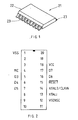
- an electronic coding device is represented generally by numeral (21) and is, in this embodiment, an integrated circuit.
- the integrated circuit comprises a small wafer of semiconductor material (not shown), such as silicon, on which an electrical circuit is produced by means any one of a number of lithographic techniques which are well known in the art.
- the semiconductor wafer is encapsulated in a rectangular block of insulating plastics or ceramic material (22) to provide a degree of structural and environmental protection. Electrical connection to the semiconductor wafer is provided by a number of metallic pins (23), each pin protruding from the encapsulating block (22) and being in electrical contact with the semiconductor wafer.
- the pins (23) are arranged in two rows on opposing sides of the encapsulating block (22). The configuration of the pins indicated in Figure 1 is utilised for surface-mounting the integrated circuit (21) to a printed circuit board (not shown).
- the pin configuration of the integrated circuit is indicated in Figure 2.
- the pins are arranged in a 20-pin dual-in-line (DIL) configuration and are individually indicated by numerals 1 to 20 in Figure 2. As indicated, only twelve of the pins are used, with the pins numbered 2, 3, 8, 9, 10, 11, 19 and 20 being unused.
- DIL dual-in-line
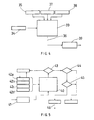
- the core of the electrical circuit is a microprocessor (24) such as the TMS370 8-bit microprocessor core available from Texas Instruments of Dallas, Texas in the USA.
- the microprocessor memory comprises 4 kilobytes of read-only memory (ROM) (25), 256 bytes of random-access memory (RAM) (26) and 256 bytes of electrically-erasable programmable read-only memory (EEPROM) (27).
- ROM read-only memory
- RAM random-access memory
- EEPROM electrically-erasable programmable read-only memory
- the ROM and EEPROM memories are non-volatile so that data stored in these memories is not lost when power is removed from the integrated circuit (21).
- a crystal oscillator and divide-by-2 clock generator (28) provides clock frequency for the micro-processor (24) while system control is provided by firmware (29).
- An input/output port (30) provides five general bidirectional input/output lines (31). The input/output lines are individually configurable under program control.
- a fuse (32) may be selectively blown to disable external read access to the ROM, RAM and EEPROM memories to protect any sensitive data which might be stored in these memories.
- the fuse (32) is usually blown only after the integrated circuit (21) has been tested for correct operation after it has been manufactured. For use in applications where power consumption is critical, the integrated circuit (21) has a stopped mode in which all of the circuit activity is stopped but data in the RAM memory (26) is maintained. Data in the non-volatile ROM (25) and EEPROM (27) memories will not be lost in any event.
- the integrated circuit (21) can only be released from the stopped mode by an externally supplied reset signal.
- the application software consists of an encryption algorithm (33) and a decryption algorithm (40).
- the integrated circuit (21) may be configured to perform either encryption or decryption by enabling either the encryption algorithm (33) or the decryption algorithm (40) respectively.
- Configuration data representing the configuration of the integrated circuit is stored in the EEPROM memory (27).
- the configuration data relates to the mode of operation of the integrated circuit, that is whether the encryption algorithm (33) or the decryption algorithm (40) has been enabled.
- Further configuration data comprises a fixed, 56-bit key value, or encryption key (34) and a variable value, or counter value (35).
- An arbitrary fixed data byte (37) is also stored in the EEPROM memory (27).
- the operation of the application software in an integrated circuit (21) which has been configured for encryption is described below.
- the encryption algorithm (33) When the encryption algorithm (33) is activated, the counter value (35) is incremented and the fixed byte (37) is appended to it.
- a checksum byte is computed from the counter value (35) and the fixed data byte (37) and is further appended to the counter value.
- the counter value (35) is 40-bits wide so that when the counter value is appended by the fixed byte (37) and the checksum byte (38), a 56-bit variable is obtained. Any algorithm may be used to compute the checksum, for example, a 16-bit cyclic redundancy check.
- the counter value, appended by the fixed and the checksum byte is encrypted together with the encryption key (34) by means of the encryption algorithm (33) to produce a unique 56-bit output value at (36).
- the output value from the encryption algorithm (33) is converted to serial form by a parallel-to-serial converter (39).
- serial data stream produced at the output of the parallel-to-serial converter (39) is transmitted by means of a radio-frequency or an infra-red transmitter front-end (not shown).
- This output data stream is configurable to conform to the timing waveform requirements of the particular transmitter type which may be used in a given application.
- up to four integrated circuits (21) configured for encryption may be linked to a single integrated circuit (21) configured for decryption, to form an operable set of devices.
- the configuration data of the decryption integrated circuit must provide for the decryption algonthm (40) to be enabled.
- each of the encryption integrated circuits must be configured with a unique encryption key (34) and with the same fixed data byte (37).
- the decryption integrated circuit is configured with the encryption key (34) of each of the linked encryption integrated circuits, up to a maximum of four such keys, and with the common fixed data byte (37).
- the decryption integrated circuit is further configured with a counter value for each of the linked encryption integrated circuits, up to a maximum of four.
- a radio-frequency of infra-red receiver acts as a front-end to the integrated circuit (21) which is configured for decryption, to receive a data stream transmitted by any one of the encryption integrated circuits.
- the receiver type is selected to match the transmitters used with the encryption integrated circuits.
- a serial data stream which is received by the receiver front-end (not shown) is converted into a received 56-bit data word by a serial-to-parallel converter (41).
- the data word is decrypted by applying the decryption algorithm (40) and a decryption key (42a).
- the decrypted data word will be a 56-bit data word made up of the counter value (35), followed by the fixed byte (37) and the checksum byte (38) which was transmitted in encrypted form as described above.
- An additional checksum byte is computed from the decrypted counter value and the decrypted fixed byte using an identical algorithm to the checksum algorithm that was used prior to encryption to compute the checksum byte (38).
- the received checksum byte and the computed checksum byte are compared at (43) and, if they are not the same, then either data corruption has occurred during transmission, or an incorrect decryption key has been used in the decryption process. If the received and computed checksum bytes do not match, the received data word is again decrypted using another decryption key (42b) stored in the EEPROM memory (27) of the decryption integrated circuit and a checksum byte is computed and compared with the received checksum byte as above.
- the process is repeated until either all the stored decryption keys (42a), (42b), (42c) and (42d) have been used for decryption, or a computed checksum byte is found which matches the received, decrypted checksum byte. If no matching checksum bytes are found in this manner, the received data is discarded and the receiver continues to listen for other transmitted streams of data.
- the received, decrypted fixed byte is compared at (44) against the fixed byte stored in the EEPROM (27) of the decryption integrated circuit. If the received and the stored fixed bytes do not match, the received data is discarded.
- the received, decrypted counter value is tested at (45) for validity against the stored counter value corresponding to the encryption key (42a), (42b), (42c) or (42d) which produced matching checksum bytes.
- the received, decrypted counter value For the received, decrypted counter value to be valid, it must be greater than the corresponding counter value stored in the decryption integrated circuit, since the counter value (35) in the encryption integrated circuit is incremented, prior to encryption and transmission.
- the received counter value must be less than the stored counter value plus a deadband of 2047, to allow for accidental or deliberate activation of the encryption integrated circuit when it is out of transmission range of the decryption integrated circuit.
- the output (46) of the decryption integrated circuit (21) may be configured to toggle between two states, equivalent to an "on” or an “off” state, or to be a pulse of selectable duration between 0,1 and 2,5 seconds.
- the output (46) may be configured to emulate the protocol of other known types of integrated circuits.
- An output signal (46) conforming to the emulated protocol is generated each time the decryption integrated circuit (21) receives a valid data stream from an encryption integrated circuit.
- Some of the protocols which may be emulated are the MC145026/VD5026 data format from Motorola of the USA, the MM53200/MM57C200 data format from National Semiconductor of the USA, or the TEA5500/1 data format from Philips of the Netherlands.
- the EEPROM memory (27) in which the configuration of the integrated circuit (21) is stored is configured by means of a programming unit (50) which may, optionally, be connected to a computer (51) such as an IBM-compatible personal computer (PC).
- the programming unit (50) comprises a micro-processor (52), a power supply (53), a keypad (54) for data entry, a liquid crystal display (LCD) (55) and a programming socket (56) to receive the integrated circuit (21).
- the programming unit (50) may be connected, at (57), to a parallel expansion socket (not shown) for external programming of additional integrated circuits (21).
- the programming unit (50) is connectable to the computer (51) through an RS232C communication port (58).
- the programming unit may be used in a stand-alone mode, in which case connection to the PC (51) is not necessary, and all configuration is performed via the keypad (54).
- Each integrated circuit (21) which is configured for encryption is configured with its own fixed unique encryption key (34) by generating a 56-bit random number in the programmer (50) and downloading this value to the EEPROM memory (27) of the integrated circuit.
- a single integrated circuit (21) configured for decryption is linked with up to four integrated circuits configured for encryption, by configuring its EEPROM memory (27) with the respective encryption keys (42a), (42b), (42c) and (42d) of the encryption integrated circuits to which it is to be linked.
- the output of an integrated circuit (21) configured for encryption may be used to cause a light-emitting-diode (LED) (not shown) to flash intermittently to provide an indication of low supply voltage.
- LED light-emitting-diode
- a warning code is transmitted by the encryption integrated circuit to the integrated circuit (21) configured for decryption, to which it is linked, and an output of the decryption integrated circuit will then be set, and this output may be used to illuminate an LED or to sound a buzzer to provide audible and visual warning of the low supply voltage.
- a similar warning code may be transmitted when an encryption integrated circuit is unable to write data to the EEPROM memory (27) due to a malfunction.
- one or more encryption integrated circuits When integrated circuits (21) are used in a motor vehicle alarm system, for example, one or more encryption integrated circuits must be linked with a single integrated circuit configured for decryption in the manner outlined above, that is, the encryption key of each encryption integrated circuit is loaded into the configuration memory of the decryption integrated circuit where it is then available for use by the decryption algorithm (40).
- the encryption integrated circuit can be made to flash an LED (not shown) to enable the optical recovery of the encryption key in an encrypted form.
- the encrypted flashes of light may be detected by a receiver and decrypted and down-loaded to a decryption integrated circuit (21). In this manner, a service station may quickly and easily reconfigure the alarm system on a motor vehicle.
- all counter values stored in the respective memories of these devices are initialised to have zero values.
- the invention therefore provides a low-cost, configurable application oriented controller suitable for use in applications requiring secure data transmission.
Landscapes
- Engineering & Computer Science (AREA)
- Theoretical Computer Science (AREA)
- General Physics & Mathematics (AREA)
- Computer Security & Cryptography (AREA)
- Physics & Mathematics (AREA)
- Software Systems (AREA)
- General Engineering & Computer Science (AREA)
- Computer Hardware Design (AREA)
- Storage Device Security (AREA)
- Communication Control (AREA)
- Error Detection And Correction (AREA)
- Selective Calling Equipment (AREA)
- Facsimile Transmission Control (AREA)
- Compression, Expansion, Code Conversion, And Decoders (AREA)
Claims (22)
- Elektronische Codiervorrichtung (21) zum selektiven Verschlüsseln oder Entschlüsseln von Datensignalen, umfassend:dadurch gekennzeichnet, daß der Konfigurationsspeicher (27) instruierbar ist, einen des vorbestimmten Verschlüsselungsalgorithmus und des vorbestimmten Entschlüsselungsalgorithmus zu wählen und das durch den Prozessor (24) erzeugte codierte digitale Ausgabesignal nach der Verschlüsselung und nach der Entschlüsselung umzuwandeln, um einem aus einer Anzahl von vorbestimmten Protokollen zu genügen.einen Prozessor (24) zum Codieren digitaler Daten in Übereinstimmung mit einem wählbaren eines vorbestimmten Verschlüsselungs- und eines vorbestimmten Entschlüsselungsalgorithmus (33, 40), wobei der Prozessor (24) einen Eingang zum Empfangen eines digitalen Eingabesignals und einen Ausgang zum Erzeugen eines codierten digitalen Ausgabesignals aufweist; undeinen mit dem Prozessor (24) verbundenen Konfigurationsspeicher (27),
- Elektronische Codiervorrichtung nach Anspruch 1, dadurch gekennzeichnet, daß der Konfigurationsspeicher (27) mittels in dem Konfigurationsspeicher gespeicherter Konfigurationsdaten instruierbar ist.
- Elektronische Codiervorrichtung nach Anspruch 2, dadurch gekennzeichnet, daß der Konfigurationsspeicher (27) ferner eine Anzahl von Schlüsselwerten (34, 42a, 42b, 42c, 42d) und eine Anzahl variabler Werte (35) enthält.
- Elektronische Codiervorrichtung nach Anspruch 3, dadurch gekennzeichnet, daß der vorbestimmte Verschlüsselungsalgorithmus (33) einen Schlüsselwert (34) und einen variablen Wert (35), die in dem Konfigurationsspeicher (27) enthalten sind, verschlüsselt, um einen verschlüsselten Wert (36) zu erzeugen.
- Elektronische Codiervorrichtung nach Anspruch 4, dadurch gekennzeichnet, daß der vorbestimmte Entschlüsselungsalgorithmus (40) einen vorher verschlüsselten Wert (36) unter Verwendung eines in dem Konfigurationsspeicher (27) enthaltenen Schlüsselwerts (42a, 42b, 42c, 42d) entschlüsselt.
- Elektronische Codiervorrichtung nach einem der Ansprüche 2 bis 5, dadurch gekennzeichnet, daß der Konfigurationsspeicher (27) mit einem Programmiermittel (50) verbindbar ist, um auf beliebige, der Konfigurationsdaten, der Schlüsselwerte und der variablen Werten in dem Konfigurationsspeicher zuzugreifen und diese zu ändern.
- Elektronische Codiervorrichtung nach einem der vorangehenden Ansprüche, dadurch gekennzeichnet, daß der Konfigurationsspeicher (27) ein nicht-flüchtiger, elektrisch löschbarer, programmierbarer Nur-LeseSpeicher ist.
- Elektronische Codiervorrichtung nach Anspruch 5, dadurch gekennzeichnet, daß eines der vorbestimmten Protokolle die Umwandlung des durch den Prozessor erzeugten codierten digitalen Ausgabesignals (36) zu einem binären Signal darstellt, das zwischen einem "Aus"-Zustand und einem "Ein"-Zustand mit einer wählbaren Frequenz alterniert.
- Elektronische Codiervorrichtung nach Anspruch 5, dadurch gekennzeichnet, daß ein anderes der vorbestimmten Protokolle die Umwandlung des durch den Prozessor erzeugten codierten digitalen Ausgabesignals (36) zu einem Puls mit wählbarer Dauer darstellt.
- Elektronische Codiervorrichtung nach Anspruch 5, dadurch gekennzeichnet, daß noch ein anderes der vorbestimmten Protokolle die Umwandlung des durch den Prozessor erzeugten codierten digitalen Ausgabesignals (36) zu einem Pulszug darstellt, der einen aus einer Anzahl verschiedener Datenformatstandards emuliert.
- Elektronische Codiervorrichtung nach einem der vorangehenden Ansprüche, dadurch gekennzeichnet, daß sie ein Mittel zum Anzeigen einer niedrigen Versorgungsspannung an der Vorrichtung umfaßt.
- Elektronische Codiervorrichtung nach Anspruch 7, dadurch gekennzeichnet, daß sie ein Mittel zum Angeben einer Fehlfunktion des nicht-flüchtigen, elektrisch löschbaren, programmierbaren Nur-Lese-Speichers enthält.
- Elektronische Codiervorrichtung nach einem der Ansprüche 3 bis 12, dadurch gekennzeichnet, daß sie ein Anzeigemittel (55) zum Anzeigen eines der in dem Konfigurationsspeicher enthaltenen Schlüsselwerte in verschlüsselter Form enthält.
- Elektronische Codiervorrichtung nach Anspruch 13, dadurch gekennzeichnet, daß das Anzeigemittel (55) eine lichtemittierende Diode ist.
- Verfahren zum Konfigurieren einer elektronischen Codiervorrichtung zum selektiven Verschlüsseln oder Entschlüsseln von Datensignalen, umfassend die Schritte:dadurch gekennzeichnet, daß es die weiteren Schritte umfaßt:Verbinden eines Programmiermittels (50) mit einem Konfigurationsspeicher (27), der mit einem Prozessor (24) zum Codieren digitaler Daten in Übereinstimmung mit einem gewählten eines vorbestimmten Verschlüsselungs- und eines vorbestimmten Entschlüsselungsalgorithmus (33, 40) verbunden ist, wobei der Prozessor (24) einen Eingang zum Empfangen eines digitalen Eingabesignals und einen Ausgang zum Erzeugen eines codierten digitalen Ausgabesignals aufweist; undInstruieren des Konfigurationsspeichers (27), einen des vorbestimmten Verschlüsselungsalgorithmus und des vorbestimmten Entschlüsselungsalgorithmus zu wählen, undInstruieren des Konfigurationsspeichers (27), das durch den Prozessor (24) erzeugte codierte digitale Ausgabesignal nach der Verschlüsselung und nach der Entschlüsselung selektiv umzuwandeln, um einem aus einer Anzahl vorbestimmter Protokolle zu genügen.
- Verfahren zum Konfigurieren einer elektronischen Codiervorrichtung nach Anspruch 15, dadurch gekennzeichnet, daß der Konfigurationsspeicher (27) durch Speichern von Konfigurationsdaten im Konfigurationsspeicher instruiert wird.
- Verfahren zum Konfigurieren einer elektronischen Codiervorrichtung nach Anspruch 16, dadurch gekennzeichnet, daß es den weiteren Schritt des Speicherns einer Anzahl von Schlüsselwerten (34, 42a, 42b, 42c, 42d) und einer Anzahl variabler Werte (35) im Konfigurationsspeicher umfaßt.
- Verfahren zum Konfigurieren einer elektronischen Codiervorrichtung nach Anspruch 17, dadurch gekennzeichnet, daß der, vorbestimmte Verschlüsselungsalgorithmus (33, 40) einen Schlüsselwert (34) und einen variablen Wert (35), die in dem Konfigurationsspeicher (27) enthalten sind, verschlüsselt, um einen verschlüsselten Wert (36) zu erzeugen.
- Verfahren zum Konfigurieren einer elektronischen Codiervorrichtung nach Anspruch 18, dadurch gekennzeichnet, daß der vorbestimmte Entschlüsselungsalgorithmus (33, 40) einen vorher verschlüsselten Wert (36) unter Verwendung eines im Konfigurationsspeichers (27) enthaltenen Schlüsselswerts (42a, 42b, 42c, 42d) entschlüsselt.
- Verfahren zum Konfigurieren einer elektronischen Codiervorrichtung nach Anspruch 19, dadurch gekennzeichnet, daß es den weiteren Schritt enthält:Verbinden einer zum Entschlüsseln konfigurierten elektronischen Codiervorrichtung (21) mit einer Anzahl von zum Verschlüsseln konfigurierten elektronischen Codiervorrichtungen (21), um einen funktionsfähigen Satz elektronischer Codiervorrichtungen zu bilden durch Speichern eines verschiedenen Schlüsselwerts (34) in den Konfigurationsspeicher (27) jeder der elektronischen Verschlüsselungs-Codiervorrichtungen und durch Speichern aller der verschiedenen Schlüsselwerte (42a, 42b, 42c, 42d) in den Konfigurationsspeicher (27) der elektronischen Entschlüsselungs-Codiervorrichtung.
- Verfahren zum Konfigurieren einer elektronischen Codiervorrichtung nach Anspruch 20, dadurch gekennzeichnet, daß es den weiteren Schritt umfaßt:Synchronisieren des funktionsfähigen Satzes von Codiervorrichtungen (21) durch Initialisieren des in dem Konfigurationsspeicher (27) jeder der elektronischen Vorrichtungen gespeicherten variablen Werts (35) auf einen bekannten vorgewählten Wert.
- Verfahren zum Konfigurieren einer elektronischen Codiervorrichtung nach Anspruch 21, dadurch gekennzeichnet, daß die Notwendigkeit zum Resynchronisieren eines funktionsfähigen Satzes elektronischer Codiervorrichtungen (21) vermieden wird, wenn die Energie von einer elektronischen Codiervorrichtung in dem Satz entfernt wird, durch Speichern der jeder elektronischen Codiervorrichtung zugeordneten Konfigurationsdaten, Schlüsselwerte (34, 42a, 42b, 42c, 42d) und variablen Werte (35) in einem jeweiligen nicht-flüchtigen Konfigurationsspeicher (27) in jeder Codiervorrichtung.
Applications Claiming Priority (4)
| Application Number | Priority Date | Filing Date | Title |
|---|---|---|---|
| ZA916493 | 1991-08-16 | ||
| ZA916493 | 1991-08-16 | ||
| ZA923306A ZA923306B (en) | 1991-08-16 | 1992-05-07 | Device for encoding or decoding of signals |
| ZA923306 | 1992-05-07 |
Publications (3)
| Publication Number | Publication Date |
|---|---|
| EP0528572A1 EP0528572A1 (de) | 1993-02-24 |
| EP0528572B1 EP0528572B1 (de) | 1997-10-15 |
| EP0528572B2 true EP0528572B2 (de) | 2005-07-06 |
Family
ID=27142102
Family Applications (1)
| Application Number | Title | Priority Date | Filing Date |
|---|---|---|---|
| EP92307041A Expired - Lifetime EP0528572B2 (de) | 1991-08-16 | 1992-08-03 | Vorrichtung zur Verschlüsselung und Entschlüsselung von Signalen |
Country Status (5)
| Country | Link |
|---|---|
| EP (1) | EP0528572B2 (de) |
| AT (1) | ATE159395T1 (de) |
| AU (1) | AU663508B2 (de) |
| DE (1) | DE69222715T3 (de) |
| ZA (1) | ZA923306B (de) |
Families Citing this family (1)
| Publication number | Priority date | Publication date | Assignee | Title |
|---|---|---|---|---|
| DE10301100A1 (de) | 2003-01-08 | 2004-07-22 | Deutsche Telekom Ag | Telekommunikationsgestützter Zeitstempel |
Family Cites Families (2)
| Publication number | Priority date | Publication date | Assignee | Title |
|---|---|---|---|---|
| US4281315A (en) * | 1979-08-27 | 1981-07-28 | Bell Telephone Laboratories, Incorporated | Collection of messages from data terminals using different protocols and formats |
| US4787028A (en) * | 1985-09-03 | 1988-11-22 | Ncr Corporation | Multicommunication protocol controller |
-
1992
- 1992-05-07 ZA ZA923306A patent/ZA923306B/xx unknown
- 1992-07-23 AU AU20520/92A patent/AU663508B2/en not_active Ceased
- 1992-08-03 DE DE69222715T patent/DE69222715T3/de not_active Expired - Fee Related
- 1992-08-03 AT AT92307041T patent/ATE159395T1/de active
- 1992-08-03 EP EP92307041A patent/EP0528572B2/de not_active Expired - Lifetime
Also Published As
| Publication number | Publication date |
|---|---|
| DE69222715D1 (de) | 1997-11-20 |
| AU2052092A (en) | 1993-02-18 |
| DE69222715T3 (de) | 2006-04-27 |
| ZA923306B (en) | 1993-01-27 |
| AU663508B2 (en) | 1995-10-12 |
| DE69222715T2 (de) | 1998-02-12 |
| EP0528572B1 (de) | 1997-10-15 |
| EP0528572A1 (de) | 1993-02-24 |
| ATE159395T1 (de) | 1997-11-15 |
Similar Documents
| Publication | Publication Date | Title |
|---|---|---|
| US4809327A (en) | Encrtption of messages employing unique control words and randomly chosen encryption keys | |
| US10341341B2 (en) | RFID authentication architecture and methods for RFID authentication | |
| US5684828A (en) | Wireless data module with two separate transmitter control outputs | |
| US6018581A (en) | Communication system and communication method | |
| JP3890510B2 (ja) | 無線周波数識別システムにおける暗号学的な認証を行なう方法 | |
| US5857025A (en) | Electronic encryption device and method | |
| US5408217A (en) | Secure fire/security/sensor transmitter system | |
| US20100208894A1 (en) | Encoder and decoder apparatus and methods | |
| KR920704463A (ko) | 선택식 호출 수신기 | |
| US5247577A (en) | Methods and apparatus for securely enabling features in highly integrated electronic circuits | |
| WO1997004395A1 (en) | Method and apparatus for encryption key creation | |
| WO1984001867A1 (en) | Method and apparatus for transmitting and receiving data messages | |
| US6725374B1 (en) | Method for the execution of an encryption program for the encryption of data in a microprocessor-based portable data carrier | |
| EP0528572B2 (de) | Vorrichtung zur Verschlüsselung und Entschlüsselung von Signalen | |
| EP0805575A2 (de) | Transponder | |
| GB2124808A (en) | Security system | |
| EP0348414A1 (de) | Übertragung und empfang von daten | |
| KR970004473A (ko) | 무선 장치 및 상기 무선 장치로의 불법적 접근 기억 시스템 및 방법 | |
| CN113091871B (zh) | 一种电子秤管理控制方法 | |
| KR20010043498A (ko) | 타이밍 장치 및 방법 | |
| RU2248292C1 (ru) | Электронная метка | |
| KR20030054340A (ko) | 코드 롬의 테스트시 데이터를 보호하기 위한 장치 | |
| US6739504B2 (en) | Method and system for ensuring connection of a module to an electronic apparatus | |
| CN109229059A (zh) | 基于keeloq加密算法的汽车遥控防盗控制系统、汽车遥控钥匙及汽车 | |
| EP0932860B1 (de) | Verfahren und system zur sicherstellung, dass mit einem elektronischen gerät verbundene module von einem bestimmten typ sind, und ein modul und ein speichermedium dafür |
Legal Events
| Date | Code | Title | Description |
|---|---|---|---|
| PUAI | Public reference made under article 153(3) epc to a published international application that has entered the european phase |
Free format text: ORIGINAL CODE: 0009012 |
|
| AK | Designated contracting states |
Kind code of ref document: A1 Designated state(s): AT BE CH DE DK ES FR GB GR IE IT LI LU MC NL PT SE |
|
| 17P | Request for examination filed |
Effective date: 19930819 |
|
| 17Q | First examination report despatched |
Effective date: 19951218 |
|
| GRAG | Despatch of communication of intention to grant |
Free format text: ORIGINAL CODE: EPIDOS AGRA |
|
| GRAH | Despatch of communication of intention to grant a patent |
Free format text: ORIGINAL CODE: EPIDOS IGRA |
|
| GRAH | Despatch of communication of intention to grant a patent |
Free format text: ORIGINAL CODE: EPIDOS IGRA |
|
| GRAA | (expected) grant |
Free format text: ORIGINAL CODE: 0009210 |
|
| AK | Designated contracting states |
Kind code of ref document: B1 Designated state(s): AT BE CH DE DK ES FR GB GR IE IT LI LU MC NL PT SE |
|
| PG25 | Lapsed in a contracting state [announced via postgrant information from national office to epo] |
Ref country code: LI Free format text: LAPSE BECAUSE OF FAILURE TO SUBMIT A TRANSLATION OF THE DESCRIPTION OR TO PAY THE FEE WITHIN THE PRESCRIBED TIME-LIMIT Effective date: 19971015 Ref country code: GR Free format text: LAPSE BECAUSE OF FAILURE TO SUBMIT A TRANSLATION OF THE DESCRIPTION OR TO PAY THE FEE WITHIN THE PRESCRIBED TIME-LIMIT Effective date: 19971015 Ref country code: FR Free format text: LAPSE BECAUSE OF FAILURE TO SUBMIT A TRANSLATION OF THE DESCRIPTION OR TO PAY THE FEE WITHIN THE PRESCRIBED TIME-LIMIT Effective date: 19971015 Ref country code: DK Free format text: LAPSE BECAUSE OF NON-PAYMENT OF DUE FEES Effective date: 19971015 Ref country code: CH Free format text: LAPSE BECAUSE OF FAILURE TO SUBMIT A TRANSLATION OF THE DESCRIPTION OR TO PAY THE FEE WITHIN THE PRESCRIBED TIME-LIMIT Effective date: 19971015 Ref country code: BE Free format text: LAPSE BECAUSE OF FAILURE TO SUBMIT A TRANSLATION OF THE DESCRIPTION OR TO PAY THE FEE WITHIN THE PRESCRIBED TIME-LIMIT Effective date: 19971015 Ref country code: AT Free format text: LAPSE BECAUSE OF FAILURE TO SUBMIT A TRANSLATION OF THE DESCRIPTION OR TO PAY THE FEE WITHIN THE PRESCRIBED TIME-LIMIT Effective date: 19971015 |
|
| REF | Corresponds to: |
Ref document number: 159395 Country of ref document: AT Date of ref document: 19971115 Kind code of ref document: T |
|
| REG | Reference to a national code |
Ref country code: CH Ref legal event code: EP |
|
| ITF | It: translation for a ep patent filed | ||
| REF | Corresponds to: |
Ref document number: 69222715 Country of ref document: DE Date of ref document: 19971120 |
|
| PG25 | Lapsed in a contracting state [announced via postgrant information from national office to epo] |
Ref country code: SE Effective date: 19980115 Ref country code: PT Free format text: LAPSE BECAUSE OF FAILURE TO SUBMIT A TRANSLATION OF THE DESCRIPTION OR TO PAY THE FEE WITHIN THE PRESCRIBED TIME-LIMIT Effective date: 19980115 |
|
| EN | Fr: translation not filed | ||
| PG25 | Lapsed in a contracting state [announced via postgrant information from national office to epo] |
Ref country code: ES Free format text: LAPSE BECAUSE OF FAILURE TO SUBMIT A TRANSLATION OF THE DESCRIPTION OR TO PAY THE FEE WITHIN THE PRESCRIBED TIME-LIMIT Effective date: 19980423 |
|
| REG | Reference to a national code |
Ref country code: CH Ref legal event code: PL |
|
| PLBI | Opposition filed |
Free format text: ORIGINAL CODE: 0009260 |
|
| PG25 | Lapsed in a contracting state [announced via postgrant information from national office to epo] |
Ref country code: LU Free format text: LAPSE BECAUSE OF NON-PAYMENT OF DUE FEES Effective date: 19980803 Ref country code: IE Free format text: LAPSE BECAUSE OF NON-PAYMENT OF DUE FEES Effective date: 19980803 |
|
| PLBF | Reply of patent proprietor to notice(s) of opposition |
Free format text: ORIGINAL CODE: EPIDOS OBSO |
|
| 26 | Opposition filed |
Opponent name: GIESECKE & DEVRIENT GMBH Effective date: 19980715 |
|
| NLR1 | Nl: opposition has been filed with the epo |
Opponent name: GIESECKE & DEVRIENT GMBH |
|
| REG | Reference to a national code |
Ref country code: GB Ref legal event code: 732E |
|
| PLBF | Reply of patent proprietor to notice(s) of opposition |
Free format text: ORIGINAL CODE: EPIDOS OBSO |
|
| NLS | Nl: assignments of ep-patents |
Owner name: CONLOG (PROPRIETARY) LIMITED |
|
| PG25 | Lapsed in a contracting state [announced via postgrant information from national office to epo] |
Ref country code: MC Free format text: LAPSE BECAUSE OF NON-PAYMENT OF DUE FEES Effective date: 19990228 |
|
| PLBF | Reply of patent proprietor to notice(s) of opposition |
Free format text: ORIGINAL CODE: EPIDOS OBSO |
|
| NLS | Nl: assignments of ep-patents |
Owner name: MERLIN GERIN S.A. (PROPRIETARY) LIMITED |
|
| REG | Reference to a national code |
Ref country code: GB Ref legal event code: 732E |
|
| RDAH | Patent revoked |
Free format text: ORIGINAL CODE: EPIDOS REVO |
|
| REG | Reference to a national code |
Ref country code: GB Ref legal event code: IF02 |
|
| APAC | Appeal dossier modified |
Free format text: ORIGINAL CODE: EPIDOS NOAPO |
|
| APAE | Appeal reference modified |
Free format text: ORIGINAL CODE: EPIDOS REFNO |
|
| APAC | Appeal dossier modified |
Free format text: ORIGINAL CODE: EPIDOS NOAPO |
|
| APBU | Appeal procedure closed |
Free format text: ORIGINAL CODE: EPIDOSNNOA9O |
|
| RAP2 | Party data changed (patent owner data changed or rights of a patent transferred) |
Owner name: MERLIN GERIN S.A. (PROPRIETARY) LIMITED Owner name: CONTROL LOGIC (PROPRIETARY) LIMITED |
|
| NLT2 | Nl: modifications (of names), taken from the european patent patent bulletin |
Owner name: MERLIN GERIN S.A. (PROPRIETARY) LIMITED |
|
| PUAH | Patent maintained in amended form |
Free format text: ORIGINAL CODE: 0009272 |
|
| STAA | Information on the status of an ep patent application or granted ep patent |
Free format text: STATUS: PATENT MAINTAINED AS AMENDED |
|
| 27A | Patent maintained in amended form |
Effective date: 20050706 |
|
| AK | Designated contracting states |
Kind code of ref document: B2 Designated state(s): AT BE CH DE DK ES FR GB GR IE IT LI LU MC NL PT SE |
|
| PG25 | Lapsed in a contracting state [announced via postgrant information from national office to epo] |
Ref country code: IT Free format text: LAPSE BECAUSE OF NON-PAYMENT OF DUE FEES;WARNING: LAPSES OF ITALIAN PATENTS WITH EFFECTIVE DATE BEFORE 2007 MAY HAVE OCCURRED AT ANY TIME BEFORE 2007. THE CORRECT EFFECTIVE DATE MAY BE DIFFERENT FROM THE ONE RECORDED. Effective date: 20050803 |
|
| REG | Reference to a national code |
Ref country code: ES Ref legal event code: FD2A Effective date: 19980804 |
|
| NLR2 | Nl: decision of opposition |
Effective date: 20050706 |
|
| NLR3 | Nl: receipt of modified translations in the netherlands language after an opposition procedure | ||
| APAH | Appeal reference modified |
Free format text: ORIGINAL CODE: EPIDOSCREFNO |
|
| EN | Fr: translation not filed | ||
| PGFP | Annual fee paid to national office [announced via postgrant information from national office to epo] |
Ref country code: NL Payment date: 20080828 Year of fee payment: 17 Ref country code: DE Payment date: 20080731 Year of fee payment: 17 |
|
| PGFP | Annual fee paid to national office [announced via postgrant information from national office to epo] |
Ref country code: GB Payment date: 20080813 Year of fee payment: 17 |
|
| REG | Reference to a national code |
Ref country code: NL Ref legal event code: V1 Effective date: 20100301 |
|
| GBPC | Gb: european patent ceased through non-payment of renewal fee |
Effective date: 20090803 |
|
| PG25 | Lapsed in a contracting state [announced via postgrant information from national office to epo] |
Ref country code: NL Free format text: LAPSE BECAUSE OF NON-PAYMENT OF DUE FEES Effective date: 20100301 Ref country code: DE Free format text: LAPSE BECAUSE OF NON-PAYMENT OF DUE FEES Effective date: 20100302 |
|
| PG25 | Lapsed in a contracting state [announced via postgrant information from national office to epo] |
Ref country code: GB Free format text: LAPSE BECAUSE OF NON-PAYMENT OF DUE FEES Effective date: 20090803 |
|
| PGFP | Annual fee paid to national office [announced via postgrant information from national office to epo] |
Ref country code: IT Payment date: 20080717 Year of fee payment: 17 |
|
| PGRI | Patent reinstated in contracting state [announced from national office to epo] |
Ref country code: IT Effective date: 20110616 |
|
| PGRI | Patent reinstated in contracting state [announced from national office to epo] |
Ref country code: IT Effective date: 20110616 |