EP0527025B1 - Circuit and method of error detection and correction in data words with checkbits - Google Patents
Circuit and method of error detection and correction in data words with checkbits Download PDFInfo
- Publication number
- EP0527025B1 EP0527025B1 EP92307060A EP92307060A EP0527025B1 EP 0527025 B1 EP0527025 B1 EP 0527025B1 EP 92307060 A EP92307060 A EP 92307060A EP 92307060 A EP92307060 A EP 92307060A EP 0527025 B1 EP0527025 B1 EP 0527025B1
- Authority
- EP
- European Patent Office
- Prior art keywords
- check bits
- error
- check
- data word
- bits
- Prior art date
- Legal status (The legal status is an assumption and is not a legal conclusion. Google has not performed a legal analysis and makes no representation as to the accuracy of the status listed.)
- Expired - Lifetime
Links
Images

Classifications
-
- G—PHYSICS
- G06—COMPUTING OR CALCULATING; COUNTING
- G06F—ELECTRIC DIGITAL DATA PROCESSING
- G06F11/00—Error detection; Error correction; Monitoring
- G06F11/07—Responding to the occurrence of a fault, e.g. fault tolerance
- G06F11/08—Error detection or correction by redundancy in data representation, e.g. by using checking codes
- G06F11/10—Adding special bits or symbols to the coded information, e.g. parity check, casting out 9's or 11's
- G06F11/1008—Adding special bits or symbols to the coded information, e.g. parity check, casting out 9's or 11's in individual solid state devices
- G06F11/1012—Adding special bits or symbols to the coded information, e.g. parity check, casting out 9's or 11's in individual solid state devices using codes or arrangements adapted for a specific type of error
- G06F11/102—Error in check bits
-
- H—ELECTRICITY
- H03—ELECTRONIC CIRCUITRY
- H03M—CODING; DECODING; CODE CONVERSION IN GENERAL
- H03M13/00—Coding, decoding or code conversion, for error detection or error correction; Coding theory basic assumptions; Coding bounds; Error probability evaluation methods; Channel models; Simulation or testing of codes
- H03M13/03—Error detection or forward error correction by redundancy in data representation, i.e. code words containing more digits than the source words
- H03M13/05—Error detection or forward error correction by redundancy in data representation, i.e. code words containing more digits than the source words using block codes, i.e. a predetermined number of check bits joined to a predetermined number of information bits
- H03M13/13—Linear codes
- H03M13/15—Cyclic codes, i.e. cyclic shifts of codewords produce other codewords, e.g. codes defined by a generator polynomial, Bose-Chaudhuri-Hocquenghem [BCH] codes
Definitions
- the present invention relates to error detection and correction circuit and method. More specifically, the present invention relates to techniques for correcting check bit errors.
- a typical memory chip is a square array of data-storage cells.
- the 64K chip for example, consists of an array of 256 by 256 data-storage cells. Each cell stores one bit, a 0 or a 1.
- the 0's and 1's stored in a memory chip are represented by the presence or absence of negative electric charge at sites in the silicon crystal. Each site has an electrical property which makes it a potential well or electronic trap for negative charge.
- the potential well at the site is filled with electrons.
- a 1 is to be stored, the well is emptied of electrons.
- the cell is read, its negative charge is measured. If the charge exceeds a certain value, the stored bit is declared to be a 0, otherwise it is declared to be a 1.
- Errors can occur when a cell loses its charge, or if an uncharged potential well acquires a charge. Hard errors occur when a given cell is stuck at 0 or stuck at 1 or toggling between 0 and 1.
- Error correcting codes help correct most errors that occur when data is stored or read from computer memories.
- Error correcting codes such as the Hamming Code, group data bits together with parity bits into a codeword using an encoding algorithm. The parity bits act as checks for the data bits. Errors occurring in the storing or reading of data bits from the computer memory are detected and corrected with a decoding algorithm.
- High speed Error Detection and Correction (EDC) chips use a Modified Hamming Code (MHC) to perform single error correction/double error detection (SEC/DED).
- MHC Modified Hamming Code
- SEC/DED single error correction/double error detection
- the MHC technique generates check bits from an input data word which are stored along with the data as a total word in memory.
- Most MHC chips read the data in from memory and generate new check bits which are compared with the check bits read from memory to generate syndrome bits.
- the syndrome bits are then ORed to determine if any errors have occurred. If a single error has occurred, the syndromes are sent through a matrix decoder which determines the location of the error. If the error occurs in the data word, the data word is corrected and output. If the error occurs in the check bits, the data is correct and can therefore be output without correction. However, any check bit error is usually ignored and an error in the check bit remains in the memory.
- EP-A-0 037 705 teaches an error correcting memory (RAM) system which corrects both data word faults and cheek bits faults. The corrected data/cheek bits are being written back into the RAM.
- RAM error correcting memory
- Check bit errors are usually detected by most error detection and correction chips and can be corrected externally. However, additional circuitry is generally required. Correcting check bit errors externally also requires additional processing time which significantly affects the performance of the chip.
- the present invention addresses the need in the art by providing a novel approach to the correction of errors in check bits in an encoded data word.
- the present invention also provides an error detection and correction method including the steps of:
- a preferred arrangement which consists of a check bit output latch which stores check bits generated by a check bit generator and outputs the newly generated check bits to memory when a single error occurs in the word, located in the check bits.
- the data is correct so the newly generated check bits are correct and can be latched out to memory at the same time the data is latched out.
- It includes a syndrome generator, an error corrector, and an error detector.
- the described arrangement provides a powerful performance boost to error detection and correction circuits by correcting check bits in memory with newly generated check bits when no errors in the data word are detected.
- Figure 1 is a schematic diagram of an illustrative implementation of a 32 bit error detection and correction circuit constructed in accordance with the teachings of the present invention.
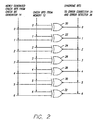
- Figure 2 is a schematic diagram of an illustrative implementation of a 7 bit syndrome generator constructed in accordance with the teachings of the present invention.
- Modified Hamming codes given a data word, generate check bits which are stored along with the data word in memory. During a read, the modified Hamming code uses the check bits to detect and locate errors.
- the Modified Hamming Code not only detects errors in the data word but in the check bits as well. Though most MHC code implementations can correct check bit errors, few MHC code implementations correct check bit errors automatically. In fact, most MHC code implementations ignore the check bit errors.
- the present embodiment provides a powerful performance boost to error detection and correction circuits by correcting check bits in memory with newly generated check bits when no errors in the data word are detected.
- a data word is read in and new check bits are generated.
- the check bits from memory are also read in and XORed with the new check bits resulting in syndrome bits.
- the syndrome bits are then decoded to locate any errors in the data word. However if a check bit is in error, the current devices signal a single bit error and output the data word unchanged. Current devices do not correct the check bit error and leave the error in the memory.
- the present embodiment makes use of the fact that the correct check bits have already been generated when there are no errors in the data bits.
- FIG. 1 is a schematic diagram of an illustrative implementation of a 32 bit error detection and correction circuit constructed in accordance with the teachings of the present invention.
- the 32 bit error detection and correction circuit of the present invention 10 consists of a memory chip 12.
- the memory chip 12 stores an encoded word which consists of a 32 bit data word and 7 check bits.
- a conventional check bit generator 14 reads the 32 bit data word from the memory chip 12 and generates 7 check bits according to a modified Hamming Code.
- a conventional check bit output latch 16 is provided which stores the 7 newly generated check bits.
- the 7 newly generated check bits are available to be written back to the memory chip 12 when the data is latched out.
- An external or internal device that determines if a check bit error or data error has occurred can be used to determine if the check bits should be written back to memory.
- the invention is implemented on a single error detection and correction chip.
- a syndrome generator 18 compares the newly generated check bits with the 7 check bits stored in the memory chip 12 and generates 7 syndrome bits.
- the syndrome generator 16 may be implemented with 7 2-bit XOR gates 20 through 32 (even numbers only). Each check bit from the memory 12 is connected to a first input of each XOR gate 20 through 32 and a corresponding check bit generated in the check bit generator 18 is connected to the second input of each XOR gate. The resulting outputs of each of the XOR gates are the syndrome bits.
- a conventional error corrector 14 connected to the output of the syndrome generator 18 reads the 32 bits from memory and outputs the corrected 32 data bits.
- a conventional error detector 36 connected to the syndrome generator 16 detects the presence of either a single bit data error, a multiple data bit error, or no data bit errors.
- the present invention has been described herein with reference to a particular embodiment for a particular application. Those having ordinary skill in the art and access to the present teachings will recognize additional modifications applications and embodiments within the scope thereof.
- the invention is not limited to a specific number of bits in the data word. Nor is it limited to a specific number of check bits. For this reason, the invention is easily adaptable to error detection and correction circuits requiring a different number of check bits.
- the described error detection and correction circuit can be modified to accommodate error detection and correction circuits using a different number of data bits or check bits without departing from the scope thereof.
- the invention is not limited to a particular error detection and correction coding scheme. Many schemes may be utilized without departing from the scope of the present teachings.
Landscapes
- Engineering & Computer Science (AREA)
- Physics & Mathematics (AREA)
- Theoretical Computer Science (AREA)
- General Physics & Mathematics (AREA)
- Algebra (AREA)
- General Engineering & Computer Science (AREA)
- Quality & Reliability (AREA)
- Mathematical Physics (AREA)
- Pure & Applied Mathematics (AREA)
- Probability & Statistics with Applications (AREA)
- Detection And Correction Of Errors (AREA)
- Detection And Prevention Of Errors In Transmission (AREA)
- Error Detection And Correction (AREA)
- Techniques For Improving Reliability Of Storages (AREA)
Abstract
Description
- The present invention relates to error detection and correction circuit and method. More specifically, the present invention relates to techniques for correcting check bit errors.
- While the present invention is described herein with reference to illustrative embodiments for particular applications, it should be understood that the invention is not limited thereto. Those having ordinary skill in the art and access to the teachings provided herein will recognize additional modifications, applications, and embodiments within the scope thereof and additional fields in which the present invention would be of significant utility.
- A typical memory chip is a square array of data-storage cells. The 64K chip, for example, consists of an array of 256 by 256 data-storage cells. Each cell stores one bit, a 0 or a 1. The 0's and 1's stored in a memory chip are represented by the presence or absence of negative electric charge at sites in the silicon crystal. Each site has an electrical property which makes it a potential well or electronic trap for negative charge. When a 0 is to be stored in a given cell, the potential well at the site is filled with electrons. When a 1 is to be stored, the well is emptied of electrons. When the cell is read, its negative charge is measured. If the charge exceeds a certain value, the stored bit is declared to be a 0, otherwise it is declared to be a 1.
- Errors can occur when a cell loses its charge, or if an uncharged potential well acquires a charge. Hard errors occur when a given cell is stuck at 0 or stuck at 1 or toggling between 0 and 1.
- Error correcting codes help correct most errors that occur when data is stored or read from computer memories. Error correcting codes, such as the Hamming Code, group data bits together with parity bits into a codeword using an encoding algorithm. The parity bits act as checks for the data bits. Errors occurring in the storing or reading of data bits from the computer memory are detected and corrected with a decoding algorithm.
- High speed Error Detection and Correction (EDC) chips use a Modified Hamming Code (MHC) to perform single error correction/double error detection (SEC/DED). The MHC technique generates check bits from an input data word which are stored along with the data as a total word in memory. Most MHC chips read the data in from memory and generate new check bits which are compared with the check bits read from memory to generate syndrome bits. The syndrome bits are then ORed to determine if any errors have occurred. If a single error has occurred, the syndromes are sent through a matrix decoder which determines the location of the error. If the error occurs in the data word, the data word is corrected and output. If the error occurs in the check bits, the data is correct and can therefore be output without correction. However, any check bit error is usually ignored and an error in the check bit remains in the memory.
- In ELECTRONIC DESIGN, vol.31, no.1, 6 January 1983, HASBROUCK HEIGTS, US, pages 269-274, W.T. GREER ET AL.: "32-bits EDAC Chips Fix Single-Bit Errors Efficiently", it is taught a conventional detection and correction system designed to correct erronous data words. The said document does not foresee the correction of faulty cheek bits.
- EP-A-0 037 705 teaches an error correcting memory (RAM) system which corrects both data word faults and cheek bits faults. The corrected data/cheek bits are being written back into the RAM.
- Check bit errors are usually detected by most error detection and correction chips and can be corrected externally. However, additional circuitry is generally required. Correcting check bit errors externally also requires additional processing time which significantly affects the performance of the chip.
- Thus, there is a need in the art for an improved system for correcting check bit errors which does not adversely affect the processing speed of the system.
- The present invention addresses the need in the art by providing a novel approach to the correction of errors in check bits in an encoded data word.
- The invention, as defined in the appended claims, provides an error detection and correction circuit comprising:
- first means for providing a data word and a first set of check bits;
- second means for generating a second set of check bits corresponding to said data word;
- third means for storing said second set of check bits; and
- fourth means connected to said first means and said second means comprising error detector means for detecting the presence of a data or check bit error and error correction means for correcting said data word and outputting a corrected data word;
- The present invention also provides an error detection and correction method including the steps of:
- providing a data word and a first set of check bits; generating a second set of check bits corresponding to said data word; and storing said second set of check bits;
- detecting the presence of an error in the said provided data word and in said check bits;
- correcting said data word in case of a detected error;
- outputting said data word;
- We will describe a preferred arrangement which consists of a check bit output latch which stores check bits generated by a check bit generator and outputs the newly generated check bits to memory when a single error occurs in the word, located in the check bits. The data is correct so the newly generated check bits are correct and can be latched out to memory at the same time the data is latched out. It includes a syndrome generator, an error corrector, and an error detector. The described arrangement provides a powerful performance boost to error detection and correction circuits by correcting check bits in memory with newly generated check bits when no errors in the data word are detected.
- Illustrative embodiments and exemplary applications will now be described with reference to the accompanying drawings to disclose the advantageous teachings of the present invention.
- Figure 1 is a schematic diagram of an illustrative implementation of a 32 bit error detection and correction circuit constructed in accordance with the teachings of the present invention.
- Figure 2 is a schematic diagram of an illustrative implementation of a 7 bit syndrome generator constructed in accordance with the teachings of the present invention.
- Modified Hamming codes, given a data word, generate check bits which are stored along with the data word in memory. During a read, the modified Hamming code uses the check bits to detect and locate errors. The Modified Hamming Code not only detects errors in the data word but in the check bits as well. Though most MHC code implementations can correct check bit errors, few MHC code implementations correct check bit errors automatically. In fact, most MHC code implementations ignore the check bit errors. The present embodiment provides a powerful performance boost to error detection and correction circuits by correcting check bits in memory with newly generated check bits when no errors in the data word are detected.
- During a read cycle a data word is read in and new check bits are generated. The check bits from memory are also read in and XORed with the new check bits resulting in syndrome bits. The syndrome bits are then decoded to locate any errors in the data word. However if a check bit is in error, the current devices signal a single bit error and output the data word unchanged. Current devices do not correct the check bit error and leave the error in the memory. The present embodiment makes use of the fact that the correct check bits have already been generated when there are no errors in the data bits.
- Figure 1 is a schematic diagram of an illustrative implementation of a 32 bit error detection and correction circuit constructed in accordance with the teachings of the present invention. In the preferred embodiment, the 32 bit error detection and correction circuit of the
present invention 10 consists of amemory chip 12. Thememory chip 12 stores an encoded word which consists of a 32 bit data word and 7 check bits. A conventionalcheck bit generator 14 reads the 32 bit data word from thememory chip 12 and generates 7 check bits according to a modified Hamming Code. - In accordance with the present teachings, a conventional check
bit output latch 16 is provided which stores the 7 newly generated check bits. The 7 newly generated check bits are available to be written back to thememory chip 12 when the data is latched out. An external or internal device that determines if a check bit error or data error has occurred can be used to determine if the check bits should be written back to memory. In the preferred embodiment, the invention is implemented on a single error detection and correction chip. - A
syndrome generator 18 compares the newly generated check bits with the 7 check bits stored in thememory chip 12 and generates 7 syndrome bits. As shown in Fig. 2, thesyndrome generator 16 may be implemented with 7 2-bit XOR gates 20 through 32 (even numbers only). Each check bit from thememory 12 is connected to a first input of eachXOR gate 20 through 32 and a corresponding check bit generated in thecheck bit generator 18 is connected to the second input of each XOR gate. The resulting outputs of each of the XOR gates are the syndrome bits. - A
conventional error corrector 14 connected to the output of thesyndrome generator 18 reads the 32 bits from memory and outputs the corrected 32 data bits. - A
conventional error detector 36 connected to thesyndrome generator 16 detects the presence of either a single bit data error, a multiple data bit error, or no data bit errors. - Thus, the present invention has been described herein with reference to a particular embodiment for a particular application. Those having ordinary skill in the art and access to the present teachings will recognize additional modifications applications and embodiments within the scope thereof. For example, the invention is not limited to a specific number of bits in the data word. Nor is it limited to a specific number of check bits. For this reason, the invention is easily adaptable to error detection and correction circuits requiring a different number of check bits. Further, the described error detection and correction circuit can be modified to accommodate error detection and correction circuits using a different number of data bits or check bits without departing from the scope thereof. In addition, the invention is not limited to a particular error detection and correction coding scheme. Many schemes may be utilized without departing from the scope of the present teachings.
- The invention is not limited to a particular logic. Functionally equivalent logic may be used wherever applicable. In some cases, reverse logic may be used without departing from the scope of the present invention.
- It is therefore intended by the appended claims to cover any and all such applications, modifications and embodiments within the scope of the present invention.
said third means including means for selectively outputting said second set of check bits on the detection of an error in the first set of check bits, wherein said third means includes a check bit output latch means and wherein the output of said third means is provided to said first means thereby correcting check bit errors.
selectively outputting said second set of check bits to replace the first set of check bits on the detection of an error in the first set of check bits, thereby correcting check bit errors.
Claims (5)
- An error detection and correction circuit (10) comprising:first means (12) for providing a data word and a first set of check bits;second means (14) for generating a second set of check bits corresponding to said data word;third means (16) for storing said second set of check bits; andfourth means (34,36) connected to said first means (12) and said second means (14) comprising error detector means (36) for detecting the presence of a data or check bit error and error correction means (34) for correcting said data word and outputting a corrected data word;characterised by
said third means (16) including means for selectively outputting said second set of check bits on the detection of an error in the first set of check bits, wherein said third means includes a check bit output latch means and wherein the output of said third means (16) is provided to said first means (12) thereby correcting check bit errors. - The circuit of claim 1, wherein said second means (14) includes a check bit generator means, connected to said data word, for generating said second set of check bits according to a modified Hamming code.
- The circuit of claim 1 or 2, wherein said fourth means (34) includes syndrome generator means (18) for generating a syndrome word.
- The circuit of claim 3, wherein said syndrome generator means (18) includes multiple input XOR gates.
- An error detection and correction method including the steps of:providing a data word and a first set of check bits; generating a second set of check bits corresponding to said data word; and storing said second set of check bits;detecting the presence of an error in the said provided data word and in said check bits;correcting said data word in case of a detected error;outputting said data word;characterised by:
selectively outputting said second set of check bits to replace the first set of check bits on the detection of an error in the first set of check bits, thereby correcting check bit errors.
Applications Claiming Priority (2)
| Application Number | Priority Date | Filing Date | Title |
|---|---|---|---|
| US74010991A | 1991-08-05 | 1991-08-05 | |
| US740109 | 1991-08-05 |
Publications (3)
| Publication Number | Publication Date |
|---|---|
| EP0527025A2 EP0527025A2 (en) | 1993-02-10 |
| EP0527025A3 EP0527025A3 (en) | 1994-01-19 |
| EP0527025B1 true EP0527025B1 (en) | 1996-12-27 |
Family
ID=24975081
Family Applications (1)
| Application Number | Title | Priority Date | Filing Date |
|---|---|---|---|
| EP92307060A Expired - Lifetime EP0527025B1 (en) | 1991-08-05 | 1992-08-03 | Circuit and method of error detection and correction in data words with checkbits |
Country Status (5)
| Country | Link |
|---|---|
| US (1) | US5633882A (en) |
| EP (1) | EP0527025B1 (en) |
| JP (1) | JPH05216698A (en) |
| AT (1) | ATE146885T1 (en) |
| DE (1) | DE69216172T2 (en) |
Families Citing this family (11)
| Publication number | Priority date | Publication date | Assignee | Title |
|---|---|---|---|---|
| US5923681A (en) * | 1998-02-24 | 1999-07-13 | Tektronix, Inc. | Parallel synchronous header correction machine for ATM |
| JP3537087B2 (en) * | 2000-09-29 | 2004-06-14 | Necエレクトロニクス株式会社 | Semiconductor device and method of inspecting semiconductor device |
| US7634709B2 (en) * | 2001-10-05 | 2009-12-15 | Unisys Corporation | Familial correction with non-familial double bit error detection |
| US6823487B1 (en) * | 2001-11-15 | 2004-11-23 | Lsi Logic Corporation | Method and apparatus for enhancing correction power of reverse order error correction codes |
| US7506226B2 (en) * | 2006-05-23 | 2009-03-17 | Micron Technology, Inc. | System and method for more efficiently using error correction codes to facilitate memory device testing |
| KR101437396B1 (en) * | 2008-02-27 | 2014-09-05 | 삼성전자주식회사 | A memory system including an error correction block capable of reducing latency and an error correction method thereof |
| US8516336B2 (en) | 2010-06-25 | 2013-08-20 | International Business Machines Corporation | Latch arrangement for an electronic digital system, method, data processing program, and computer program product for implementing a latch arrangement |
| US8612834B2 (en) * | 2011-03-08 | 2013-12-17 | Intel Corporation | Apparatus, system, and method for decoding linear block codes in a memory controller |
| RU2448359C1 (en) * | 2011-04-05 | 2012-04-20 | Межрегиональное общественное учреждение "Институт инженерной физики" | Apparatus for storing and transmitting data with error correction in data byte and error detection in data bytes |
| RU2534499C2 (en) * | 2013-03-25 | 2014-11-27 | Межрегиональное общественное учреждение "Институт инженерной физики" | Data storage and transmission device with error correction in two information bytes |
| CN110532127B (en) * | 2019-08-13 | 2023-03-03 | 南京芯驰半导体科技有限公司 | A Protocol Converter for Error Checking Bits |
Family Cites Families (14)
| Publication number | Priority date | Publication date | Assignee | Title |
|---|---|---|---|---|
| US4277844A (en) * | 1979-07-26 | 1981-07-07 | Storage Technology Corporation | Method of detecting and correcting errors in digital data storage systems |
| US4271519A (en) * | 1979-07-26 | 1981-06-02 | Storage Technology Corporation | Address mark generation and decoding method |
| US4317201A (en) * | 1980-04-01 | 1982-02-23 | Honeywell, Inc. | Error detecting and correcting RAM assembly |
| US4334309A (en) * | 1980-06-30 | 1982-06-08 | International Business Machines Corporation | Error correcting code system |
| US4412329A (en) * | 1981-10-15 | 1983-10-25 | Sri International | Parity bit lock-on method and apparatus |
| US4612640A (en) * | 1984-02-21 | 1986-09-16 | Seeq Technology, Inc. | Error checking and correction circuitry for use with an electrically-programmable and electrically-erasable memory array |
| US4646312A (en) * | 1984-12-13 | 1987-02-24 | Ncr Corporation | Error detection and correction system |
| US4730320A (en) * | 1985-02-07 | 1988-03-08 | Mitsubishi Denki Kabushiki Kaisha | Semiconductor memory device |
| US4737830A (en) * | 1986-01-08 | 1988-04-12 | Advanced Micro Devices, Inc. | Integrated circuit structure having compensating means for self-inductance effects |
| JPS62251949A (en) * | 1986-04-25 | 1987-11-02 | Mitsubishi Electric Corp | Error correcting method for memory device |
| US4817095A (en) * | 1987-05-15 | 1989-03-28 | Digital Equipment Corporation | Byte write error code method and apparatus |
| JP2583547B2 (en) * | 1988-01-13 | 1997-02-19 | 株式会社日立製作所 | Semiconductor memory |
| US4993028A (en) * | 1988-09-07 | 1991-02-12 | Thinking Machines Corporation | Error detection and correction coding |
| US5014273A (en) * | 1989-01-27 | 1991-05-07 | Digital Equipment Corporation | Bad data algorithm |
-
1992
- 1992-07-09 JP JP4181395A patent/JPH05216698A/en not_active Withdrawn
- 1992-08-03 EP EP92307060A patent/EP0527025B1/en not_active Expired - Lifetime
- 1992-08-03 DE DE69216172T patent/DE69216172T2/en not_active Expired - Fee Related
- 1992-08-03 AT AT92307060T patent/ATE146885T1/en active
-
1996
- 1996-03-11 US US08/615,033 patent/US5633882A/en not_active Expired - Fee Related
Also Published As
| Publication number | Publication date |
|---|---|
| DE69216172D1 (en) | 1997-02-06 |
| EP0527025A3 (en) | 1994-01-19 |
| DE69216172T2 (en) | 1997-05-07 |
| ATE146885T1 (en) | 1997-01-15 |
| JPH05216698A (en) | 1993-08-27 |
| EP0527025A2 (en) | 1993-02-10 |
| US5633882A (en) | 1997-05-27 |
Similar Documents
| Publication | Publication Date | Title |
|---|---|---|
| JP3325914B2 (en) | Error correction detection method for data and error detection circuit for computer memory | |
| US5418796A (en) | Synergistic multiple bit error correction for memory of array chips | |
| EP2203819B1 (en) | Semiconductor memory device and its control method | |
| US6041430A (en) | Error detection and correction code for data and check code fields | |
| US7992071B2 (en) | Method for implementing error-correction codes in non-volatile memory | |
| US5251219A (en) | Error detection and correction circuit | |
| US7231585B2 (en) | Error correction for flash memory | |
| US20160041875A1 (en) | Semiconductor memory device and method of controlling the same | |
| US5751744A (en) | Error detection and correction circuit | |
| US7890846B2 (en) | Electronic data flash card with Reed Solomon error detection and correction capability | |
| JPH11312396A (en) | Multi-bit semiconductor memory device and error correction method for the device | |
| JPH0260013B2 (en) | ||
| EP0147336A2 (en) | Error correcting and detecting system | |
| US10191801B2 (en) | Error correction code management of write-once memory codes | |
| US5751745A (en) | Memory implemented error detection and correction code with address parity bits | |
| US5633882A (en) | Error detection and correction circuit | |
| US20220190846A1 (en) | Single error correct double error detect (secded) error coding with burst error detection capability | |
| US5761221A (en) | Memory implemented error detection and correction code using memory modules | |
| JPH0736717A (en) | Error correcting method and apparatus for detecting single symbol error and single-bit error | |
| US7213191B2 (en) | System and method for securely storing data in a memory | |
| US8196011B2 (en) | Error detection and correction circuit and semiconductor memory | |
| EP0793173B1 (en) | Non-volatile semiconductor storage unit having a correction coding circuit | |
| US20020174397A1 (en) | Method for error detection/correction of multilevel cell memory and multilevel cell memory having error detection/correction function | |
| JPH11213692A (en) | Memory device | |
| JPH11212876A (en) | Encoding method and memory device using the same |
Legal Events
| Date | Code | Title | Description |
|---|---|---|---|
| PUAI | Public reference made under article 153(3) epc to a published international application that has entered the european phase |
Free format text: ORIGINAL CODE: 0009012 |
|
| AK | Designated contracting states |
Kind code of ref document: A2 Designated state(s): AT BE CH DE DK ES FR GB GR IE IT LI LU NL PT SE |
|
| PUAL | Search report despatched |
Free format text: ORIGINAL CODE: 0009013 |
|
| AK | Designated contracting states |
Kind code of ref document: A3 Designated state(s): AT BE CH DE DK ES FR GB GR IE IT LI LU NL PT SE |
|
| 17P | Request for examination filed |
Effective date: 19940421 |
|
| 17Q | First examination report despatched |
Effective date: 19950519 |
|
| GRAG | Despatch of communication of intention to grant |
Free format text: ORIGINAL CODE: EPIDOS AGRA |
|
| GRAH | Despatch of communication of intention to grant a patent |
Free format text: ORIGINAL CODE: EPIDOS IGRA |
|
| GRAH | Despatch of communication of intention to grant a patent |
Free format text: ORIGINAL CODE: EPIDOS IGRA |
|
| GRAA | (expected) grant |
Free format text: ORIGINAL CODE: 0009210 |
|
| AK | Designated contracting states |
Kind code of ref document: B1 Designated state(s): AT BE CH DE DK ES FR GB GR IE IT LI LU NL PT SE |
|
| PG25 | Lapsed in a contracting state [announced via postgrant information from national office to epo] |
Ref country code: NL Free format text: LAPSE BECAUSE OF FAILURE TO SUBMIT A TRANSLATION OF THE DESCRIPTION OR TO PAY THE FEE WITHIN THE PRESCRIBED TIME-LIMIT Effective date: 19961227 Ref country code: LI Effective date: 19961227 Ref country code: IT Free format text: LAPSE BECAUSE OF FAILURE TO SUBMIT A TRANSLATION OF THE DESCRIPTION OR TO PAY THE FEE WITHIN THE PRESCRIBED TIME-LIMIT;WARNING: LAPSES OF ITALIAN PATENTS WITH EFFECTIVE DATE BEFORE 2007 MAY HAVE OCCURRED AT ANY TIME BEFORE 2007. THE CORRECT EFFECTIVE DATE MAY BE DIFFERENT FROM THE ONE RECORDED. Effective date: 19961227 Ref country code: GR Free format text: LAPSE BECAUSE OF FAILURE TO SUBMIT A TRANSLATION OF THE DESCRIPTION OR TO PAY THE FEE WITHIN THE PRESCRIBED TIME-LIMIT Effective date: 19961227 Ref country code: FR Effective date: 19961227 Ref country code: ES Free format text: THE PATENT HAS BEEN ANNULLED BY A DECISION OF A NATIONAL AUTHORITY Effective date: 19961227 Ref country code: DK Effective date: 19961227 Ref country code: CH Effective date: 19961227 Ref country code: BE Effective date: 19961227 Ref country code: AT Effective date: 19961227 |
|
| REF | Corresponds to: |
Ref document number: 146885 Country of ref document: AT Date of ref document: 19970115 Kind code of ref document: T |
|
| REF | Corresponds to: |
Ref document number: 69216172 Country of ref document: DE Date of ref document: 19970206 |
|
| REG | Reference to a national code |
Ref country code: IE Ref legal event code: FG4D Free format text: 71228 |
|
| PG25 | Lapsed in a contracting state [announced via postgrant information from national office to epo] |
Ref country code: SE Effective date: 19970327 Ref country code: PT Effective date: 19970327 |
|
| EN | Fr: translation not filed | ||
| NLV1 | Nl: lapsed or annulled due to failure to fulfill the requirements of art. 29p and 29m of the patents act | ||
| REG | Reference to a national code |
Ref country code: CH Ref legal event code: PL |
|
| PG25 | Lapsed in a contracting state [announced via postgrant information from national office to epo] |
Ref country code: IE Free format text: LAPSE BECAUSE OF NON-PAYMENT OF DUE FEES Effective date: 19970803 |
|
| PG25 | Lapsed in a contracting state [announced via postgrant information from national office to epo] |
Ref country code: LU Free format text: LAPSE BECAUSE OF NON-PAYMENT OF DUE FEES Effective date: 19970831 |
|
| PLBE | No opposition filed within time limit |
Free format text: ORIGINAL CODE: 0009261 |
|
| STAA | Information on the status of an ep patent application or granted ep patent |
Free format text: STATUS: NO OPPOSITION FILED WITHIN TIME LIMIT |
|
| 26N | No opposition filed | ||
| PGFP | Annual fee paid to national office [announced via postgrant information from national office to epo] |
Ref country code: GB Payment date: 19980702 Year of fee payment: 7 |
|
| PGFP | Annual fee paid to national office [announced via postgrant information from national office to epo] |
Ref country code: DE Payment date: 19980827 Year of fee payment: 7 |
|
| PG25 | Lapsed in a contracting state [announced via postgrant information from national office to epo] |
Ref country code: GB Free format text: LAPSE BECAUSE OF NON-PAYMENT OF DUE FEES Effective date: 19990803 |
|
| GBPC | Gb: european patent ceased through non-payment of renewal fee |
Effective date: 19990803 |
|
| PG25 | Lapsed in a contracting state [announced via postgrant information from national office to epo] |
Ref country code: DE Free format text: LAPSE BECAUSE OF NON-PAYMENT OF DUE FEES Effective date: 20000601 |