EP0523318B1 - Light-emitting device - Google Patents
Light-emitting device Download PDFInfo
- Publication number
- EP0523318B1 EP0523318B1 EP92104501A EP92104501A EP0523318B1 EP 0523318 B1 EP0523318 B1 EP 0523318B1 EP 92104501 A EP92104501 A EP 92104501A EP 92104501 A EP92104501 A EP 92104501A EP 0523318 B1 EP0523318 B1 EP 0523318B1
- Authority
- EP
- European Patent Office
- Prior art keywords
- substrate
- rear panel
- light emitting
- electrode leads
- emitting device
- Prior art date
- Legal status (The legal status is an assumption and is not a legal conclusion. Google has not performed a legal analysis and makes no representation as to the accuracy of the status listed.)
- Expired - Lifetime
Links
Images


Classifications
-
- H—ELECTRICITY
- H01—ELECTRIC ELEMENTS
- H01J—ELECTRIC DISCHARGE TUBES OR DISCHARGE LAMPS
- H01J31/00—Cathode ray tubes; Electron beam tubes
- H01J31/08—Cathode ray tubes; Electron beam tubes having a screen on or from which an image or pattern is formed, picked up, converted, or stored
- H01J31/10—Image or pattern display tubes, i.e. having electrical input and optical output; Flying-spot tubes for scanning purposes
- H01J31/12—Image or pattern display tubes, i.e. having electrical input and optical output; Flying-spot tubes for scanning purposes with luminescent screen
- H01J31/15—Image or pattern display tubes, i.e. having electrical input and optical output; Flying-spot tubes for scanning purposes with luminescent screen with ray or beam selectively directed to luminescent anode segments
-
- H—ELECTRICITY
- H01—ELECTRIC ELEMENTS
- H01J—ELECTRIC DISCHARGE TUBES OR DISCHARGE LAMPS
- H01J29/00—Details of cathode-ray tubes or of electron-beam tubes of the types covered by group H01J31/00
- H01J29/02—Electrodes; Screens; Mounting, supporting, spacing or insulating thereof
- H01J29/08—Electrodes intimately associated with a screen on or from which an image or pattern is formed, picked-up, converted or stored, e.g. backing-plates for storage tubes or collecting secondary electrons
- H01J29/085—Anode plates, e.g. for screens of flat panel displays
-
- H—ELECTRICITY
- H01—ELECTRIC ELEMENTS
- H01J—ELECTRIC DISCHARGE TUBES OR DISCHARGE LAMPS
- H01J29/00—Details of cathode-ray tubes or of electron-beam tubes of the types covered by group H01J31/00
- H01J29/86—Vessels; Containers; Vacuum locks
-
- H—ELECTRICITY
- H01—ELECTRIC ELEMENTS
- H01J—ELECTRIC DISCHARGE TUBES OR DISCHARGE LAMPS
- H01J29/00—Details of cathode-ray tubes or of electron-beam tubes of the types covered by group H01J31/00
- H01J29/92—Means forming part of the tube for the purpose of providing electrical connection to it
-
- H—ELECTRICITY
- H01—ELECTRIC ELEMENTS
- H01J—ELECTRIC DISCHARGE TUBES OR DISCHARGE LAMPS
- H01J31/00—Cathode ray tubes; Electron beam tubes
- H01J31/08—Cathode ray tubes; Electron beam tubes having a screen on or from which an image or pattern is formed, picked up, converted, or stored
- H01J31/10—Image or pattern display tubes, i.e. having electrical input and optical output; Flying-spot tubes for scanning purposes
- H01J31/12—Image or pattern display tubes, i.e. having electrical input and optical output; Flying-spot tubes for scanning purposes with luminescent screen
- H01J31/123—Flat display tubes
-
- H—ELECTRICITY
- H01—ELECTRIC ELEMENTS
- H01J—ELECTRIC DISCHARGE TUBES OR DISCHARGE LAMPS
- H01J9/00—Apparatus or processes specially adapted for the manufacture, installation, removal, maintenance of electric discharge tubes, discharge lamps, or parts thereof; Recovery of material from discharge tubes or lamps
- H01J9/24—Manufacture or joining of vessels, leading-in conductors or bases
- H01J9/26—Sealing together parts of vessels
- H01J9/261—Sealing together parts of vessels the vessel being for a flat panel display
Definitions
- the present invention relates to a light emitting device as a constituent member of a large screen apparatus used in a stadium or the like.
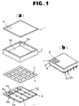
- Fig. 1(a) is an exploded perspective view of a conventional light emitting device disclosed in Japanese Patent Laid Open No. 100854/89 for example.
- the reference numeral 1 denotes a front panel on which are arranged fluorescent elements 2 in a matrix form and which covers one opening portion of a square frame-like spacer 3;
- the numeral 4 denotes a shielding electrode having openings 5 in corresponding relation to the fluorescent elements 2 arranged on the front panel 1;
- numeral 6 denotes a rear panel having cathodes 7 arranged thereon in corresponding relation to the fluorescent elements 2 to emit thermoelectrons for causing the fluorescent elements 2 arranged on the front panel 1 to emit light, the rear panel 6 covering the other opening portion of the spacer 3;
- numeral 8a denotes a first control eleetrode (scan electrode) for the cathodes 7;
- numeral 8b denotes a second control electrode (data electrode) for the cathode 7;
- numerals 9a and 9b
- a space 3a surrounded by the spacer 3 will be designated the interior of the spacer, and each inside wall surface 3b will be referred to as the inner side face.
- the front panel 1 also serves as an anode. In the case where the front panel 1 does not serve as an anode, an anode is disposed between the front panel and the shielding electrode 4.
- Fig. 6 shows an example of a display comprising a number of light emitting devices A1, A2. It is seen from this figure that in order to make the joint portion between adjacent light emitting devices A1 and A2 inconspicuous, it is necessary to provide between adjacent light emitting elements 2 in each light emitting device a space T2 which is twice or more as large as a dead space (width T1) provided around the light emitting device.
- Fig. 8 shows an example in which cathodes 7, etc. are provided on a ceramic substrate 13, not on the rear panel 6.
- scan electrodes 8a and data electrodes 8b are drawn out to the exterior through both the ceramic substrate 13 and the rear panel 6.
- the numeral 14 denotes a shielding electrode.
- the openings of the shielding electrode 4 which emit electrons are influenced by static electricity of the inner side faces of the spacer 3. Since the inner side faces of the spacer 3 are positively charged, if the openings of the shielding electrode 4 approach the spacer 3 due to displacement of the rear panel 6, the openings are strongly influenced by the positive potential of the inner side faces of the spacer 3, whereby the emission of electrons is accelerated. As a result, the luminance of the corresponding fluorescent element increases. On the other hand, as the said openings go away from the spacer 3, the luminance decreases. Thus, in the interior of the light emitting device there occur variations in luminance.
- the present invention as defined in Claim 1 is a light emitting device having first electrode leads the first electrode leads having a thermal expansion coefficient equal to that of a substrate, inserted into the substrate to support the substrate and connected to control electrodes for cathodes arranged on the substrate, and also having second electrode leads the second electrode leads having a thermal expansion coefficient equal to that of a rear panel, inserted into the rear panel and connected to the first electrode lead.
- the gap between the substrate and the rear panel absorbs a stress induced in the substrate because of the difference in thermal expansion coefficient between the substrate and the rear panel.
- Fig. 4(a) is an exploded perspective view of a light emitting element according to an embodiment of the present invention
- Fig. 4(b) is a perspective view of the light emitting element as assembled
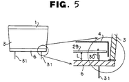
- Fig. 5 is a sectional view of the light emitting device illustrated in Fig. 4(b).
- numeral 29 denotes a ceramic substrate inserted in the vicinity of a rear panel 6 in the interior of a spacer 3 and with thermoelectron emitting cathodes being arranged thereon in corresponding relation to fluorescent elements 2 arranged on a front panel 1 for causing the fluorescent elements to emit light;
- numeral 30 denotes a first electrode lead having a thermal expansion coefficient equal to that of the ceramic substrate 29, extending through the ceramic substrate to support the same substrate and connected to scan electrodes 8a and data electrodes 8b for the cathodes arranged on the ceramic substrate 29;
- numeral 31 denotes a second electrode lead having a thermal expansion coefficient equal to that of the rear panel 6, inserted into the rear panel and connected to the first electrode lead 30.
- the first electrode leads 30 having a thermal expansion coefficient equal to that of the ceramic substrate 29 are connected through the ceramic substrate 29 to the scan electrodes 8a and data electrodes 8b.
- the second electrode leads 31 having a thermal expansion coefficient equal to that of the rear panel 6 are connected through the rear panel to the first electrode leads 30.
- the ceramic substrate 29 is mounted in a floating state at a distance of gap L from the rear panel 6 through the first electrode leads 30. In this state, a stress induced due to the difference in thermal expansion coefficient between the ceramic substrate 29 and the rear panel 6 is absorbed by the gap L. Therefore, even if the second electrode leads 31 pass through the rear panel, there arises no inconvenience.
- the electrode leads of the light emitting devices be drawn out through the rear panel 6 rather than drawn out from the sealed portion between the spacer 3 and the rear panel 6, because the spacing between adjacent light emitting devices can be narrowed.
- the correlation between the cathodes 7 and the fluorescent elements 2 is 1 : 2, it may be 1 : 1 or 1 : n.
- the present invention is also applicable to light emitting devices based on the principle of a discharge tube or the like.
Landscapes
- Engineering & Computer Science (AREA)
- Manufacturing & Machinery (AREA)
- Cathode-Ray Tubes And Fluorescent Screens For Display (AREA)
- Vessels, Lead-In Wires, Accessory Apparatuses For Cathode-Ray Tubes (AREA)
Description
- The present invention relates to a light emitting device as a constituent member of a large screen apparatus used in a stadium or the like.
- Fig. 1(a) is an exploded perspective view of a conventional light emitting device disclosed in Japanese Patent Laid Open No. 100854/89 for example. In the same figure, the
reference numeral 1 denotes a front panel on which are arrangedfluorescent elements 2 in a matrix form and which covers one opening portion of a square frame-like spacer 3; thenumeral 4 denotes a shieldingelectrode having openings 5 in corresponding relation to thefluorescent elements 2 arranged on thefront panel 1;numeral 6 denotes a rearpanel having cathodes 7 arranged thereon in corresponding relation to thefluorescent elements 2 to emit thermoelectrons for causing thefluorescent elements 2 arranged on thefront panel 1 to emit light, therear panel 6 covering the other opening portion of thespacer 3;numeral 8a denotes a first control eleetrode (scan electrode) for thecathodes 7;numeral 8b denotes a second control electrode (data electrode) for thecathode 7;numerals 9a and 9b denote wiring patterns for connecting thescan electrodes 8a anddata electrodes 8b in common in the direction of row or column; andnumeral 10 denotes an exhaust portion. Hereinafter, aspace 3a surrounded by thespacer 3 will be designated the interior of the spacer, and each insidewall surface 3b will be referred to as the inner side face. In some case, thefront panel 1 also serves as an anode. In the case where thefront panel 1 does not serve as an anode, an anode is disposed between the front panel and theshielding electrode 4. - Fig. 6 shows an example of a display comprising a number of light emitting devices A1, A2. It is seen from this figure that in order to make the joint portion between adjacent light emitting devices A1 and A2 inconspicuous, it is necessary to provide between adjacent
light emitting elements 2 in each light emitting device a space T2 which is twice or more as large as a dead space (width T1) provided around the light emitting device. - Fig. 8 shows an example in which
cathodes 7, etc. are provided on aceramic substrate 13, not on therear panel 6. In this case,scan electrodes 8a anddata electrodes 8b are drawn out to the exterior through both theceramic substrate 13 and therear panel 6. Thenumeral 14 denotes a shielding electrode. - There may arise further problems such as deterioration of the mechanical accuracy and variations in luminance. The openings of the
shielding electrode 4 which emit electrons are influenced by static electricity of the inner side faces of thespacer 3. Since the inner side faces of thespacer 3 are positively charged, if the openings of theshielding electrode 4 approach thespacer 3 due to displacement of therear panel 6, the openings are strongly influenced by the positive potential of the inner side faces of thespacer 3, whereby the emission of electrons is accelerated. As a result, the luminance of the corresponding fluorescent element increases. On the other hand, as the said openings go away from thespacer 3, the luminance decreases. Thus, in the interior of the light emitting device there occur variations in luminance. - In the case where the
scan electrodes 8a anddata electrodes 8b are drawn out to the exterior through theceramic substrate 13 and therear panel 6, as shown in Fig. 8, a stress is induced in theceramic substrate 13 due to the difference in thermal expansion coefficient among theceramic substrate 13,rear panel 6,scan electrodes 8a anddata electrodes 8b, resulting in cracking of the ceramic substrate. - From US-A-4,935,583 an insulated conductor is known which is bonded to a ceramic isolator. To avoid destruction of the bond due to temperature variations the thermal expansion coefficiant of the isolator and the conductor are substantially equal.
- Thus it is an object of the present invention to provide a light emitting device having a substrate with reduced stress induced when subjected to thermal variations to thereby obtain a light emitting device of high accuracy free of variations, in luminance and reduce the dead space between light emitting devices A1 and A2, thereby affording a display of high resolution.
- The present invention as defined in
Claim 1 is a light emitting device having first electrode leads the first electrode leads having a thermal expansion coefficient equal to that of a substrate, inserted into the substrate to support the substrate and connected to control electrodes for cathodes arranged on the substrate, and also having second electrode leads the second electrode leads having a thermal expansion coefficient equal to that of a rear panel, inserted into the rear panel and connected to the first electrode lead. In this light emitting device, the gap between the substrate and the rear panel absorbs a stress induced in the substrate because of the difference in thermal expansion coefficient between the substrate and the rear panel. -
- Fig. 1 is an exploded perspective view of a conventional light emitting device;
- Fig. 2 is an explanatory view showing two adjacent light emitting devices;
- Fig. 3 is a sectional view of a conventional light emitting device having a ceramic substrate;
- Fig. 4 is an exploded perspective view of a light emitting device according to a sixth embodiment of the present invention; and
- Fig. 5 is a sectional view thereof.
- Fig. 4(a) is an exploded perspective view of a light emitting element according to an embodiment of the present invention, Fig. 4(b) is a perspective view of the light emitting element as assembled, and Fig. 5 is a sectional view of the light emitting device illustrated in Fig. 4(b). In these figures,
numeral 29 denotes a ceramic substrate inserted in the vicinity of arear panel 6 in the interior of aspacer 3 and with thermoelectron emitting cathodes being arranged thereon in corresponding relation tofluorescent elements 2 arranged on afront panel 1 for causing the fluorescent elements to emit light; numeral 30 denotes a first electrode lead having a thermal expansion coefficient equal to that of theceramic substrate 29, extending through the ceramic substrate to support the same substrate and connected toscan electrodes 8a anddata electrodes 8b for the cathodes arranged on theceramic substrate 29; andnumeral 31 denotes a second electrode lead having a thermal expansion coefficient equal to that of therear panel 6, inserted into the rear panel and connected to the first electrode lead 30. - The operation of this light emitting device will be described below.
- First, the first electrode leads 30 having a thermal expansion coefficient equal to that of the
ceramic substrate 29 are connected through theceramic substrate 29 to thescan electrodes 8a anddata electrodes 8b. Next, the second electrode leads 31 having a thermal expansion coefficient equal to that of therear panel 6 are connected through the rear panel to the first electrode leads 30. At this time, theceramic substrate 29 is mounted in a floating state at a distance of gap L from therear panel 6 through the first electrode leads 30. In this state, a stress induced due to the difference in thermal expansion coefficient between theceramic substrate 29 and therear panel 6 is absorbed by the gap L. Therefore, even if the second electrode leads 31 pass through the rear panel, there arises no inconvenience. For arranging light emitting devices closely to each other, it is preferable that the electrode leads of the light emitting devices be drawn out through therear panel 6 rather than drawn out from the sealed portion between thespacer 3 and therear panel 6, because the spacing between adjacent light emitting devices can be narrowed. - Although in the above embodiments, the correlation between the
cathodes 7 and thefluorescent elements 2 is 1 : 2, it may be 1 : 1 or 1 : n. - Further, although the light emitting devices described in the above embodiments are based on the CRT principle, the present invention is also applicable to light emitting devices based on the principle of a discharge tube or the like.
- In the case where the first electrode leads having a thermal expansion coefficient equal to that of the substrate and the second electrode leads having a thermal expansion coefficient equal to that of the rear panel are connected together, a stress induced due to the difference in thermal expansion coefficient between the substrate and the rear panel is absorbed at the portion of the gap L, so even when the second electrode leads are provided through the rear panel, there will arise no inconvenience such as cracking of the substrate for example, thus permitting a closely-spaced arrangement of light emitting devices.
Claims (3)
- A light emitting device includinga front panel (1) on which fluorescent elements (2) are arranged in a matrix form;a substrate (29) on which cathodes (7) are arranged in a corresponding relation to said fluorescent elements (2), said cathodes (7) emitting thermoelectrons for causing the fluorescent elements (2) to emit light;a square frame-like spacer (3), one opening portion of said spacer (3) being covered with said front panel (1) and the other opening portion thereof covered with a rear panel (6);first electrode leads (30) having a thermal expansion coefficient equal to that of said substrate (29), said first electrode leads (30) being inserted into said substrate (29) to support the substrate (29) and connected to control electrodes (8a, 8b) for said cathodes (7) arranged on the substrate (29); andsecond electrode leads (31) having a thermal expansion coefficient equal to that of said rear panel (6), said second electrode leads (31) being inserted into said rear panel (6) and connected to said first electrode leads (30).
- A light emitting device according to claim 1, wherein said substrate (29) is held at a predetermined distance from said rear panel (6) by means of said first (30) and second electrode leads (31).
- A light emitting device according to claim 1 or 2, wherein said thermal expansion coefficient of said first electrode leads (30) and said substrate (29) is different from said thermal expansion coefficient of said second electrode leads (31) and said rear panel (6).
Priority Applications (1)
| Application Number | Priority Date | Filing Date | Title |
|---|---|---|---|
| EP95111009A EP0678893B1 (en) | 1991-07-16 | 1992-03-16 | Light emitting device |
Applications Claiming Priority (2)
| Application Number | Priority Date | Filing Date | Title |
|---|---|---|---|
| JP3174899A JP2804392B2 (en) | 1991-07-16 | 1991-07-16 | Light emitting device and manufacturing method thereof |
| JP174899/91 | 1991-07-16 |
Related Child Applications (2)
| Application Number | Title | Priority Date | Filing Date |
|---|---|---|---|
| EP95111009A Division EP0678893B1 (en) | 1991-07-16 | 1992-03-16 | Light emitting device |
| EP95111009.7 Division-Into | 1992-03-16 |
Publications (3)
| Publication Number | Publication Date |
|---|---|
| EP0523318A2 EP0523318A2 (en) | 1993-01-20 |
| EP0523318A3 EP0523318A3 (en) | 1993-03-17 |
| EP0523318B1 true EP0523318B1 (en) | 1996-01-31 |
Family
ID=15986638
Family Applications (4)
| Application Number | Title | Priority Date | Filing Date |
|---|---|---|---|
| EP97122187A Withdrawn EP0834903A1 (en) | 1991-07-16 | 1992-03-16 | Light emitting device |
| EP95111009A Expired - Lifetime EP0678893B1 (en) | 1991-07-16 | 1992-03-16 | Light emitting device |
| EP92104501A Expired - Lifetime EP0523318B1 (en) | 1991-07-16 | 1992-03-16 | Light-emitting device |
| EP97122188A Withdrawn EP0855732A1 (en) | 1991-07-16 | 1992-03-16 | Light emitting device |
Family Applications Before (2)
| Application Number | Title | Priority Date | Filing Date |
|---|---|---|---|
| EP97122187A Withdrawn EP0834903A1 (en) | 1991-07-16 | 1992-03-16 | Light emitting device |
| EP95111009A Expired - Lifetime EP0678893B1 (en) | 1991-07-16 | 1992-03-16 | Light emitting device |
Family Applications After (1)
| Application Number | Title | Priority Date | Filing Date |
|---|---|---|---|
| EP97122188A Withdrawn EP0855732A1 (en) | 1991-07-16 | 1992-03-16 | Light emitting device |
Country Status (4)
| Country | Link |
|---|---|
| US (3) | US5304083A (en) |
| EP (4) | EP0834903A1 (en) |
| JP (1) | JP2804392B2 (en) |
| DE (2) | DE69226290T2 (en) |
Families Citing this family (17)
| Publication number | Priority date | Publication date | Assignee | Title |
|---|---|---|---|---|
| JP2568633Y2 (en) * | 1993-05-27 | 1998-04-15 | 双葉電子工業株式会社 | Fluorescent tube |
| JP3426340B2 (en) * | 1994-05-30 | 2003-07-14 | ノリタケ伊勢電子株式会社 | Display tube for light source and method of manufacturing the same |
| US5629583A (en) * | 1994-07-25 | 1997-05-13 | Fed Corporation | Flat panel display assembly comprising photoformed spacer structure, and method of making the same |
| JP3624041B2 (en) * | 1995-01-06 | 2005-02-23 | キヤノン株式会社 | Image display device using conductive frit |
| US5688158A (en) * | 1995-08-24 | 1997-11-18 | Fed Corporation | Planarizing process for field emitter displays and other electron source applications |
| US5828288A (en) * | 1995-08-24 | 1998-10-27 | Fed Corporation | Pedestal edge emitter and non-linear current limiters for field emitter displays and other electron source applications |
| US5844351A (en) * | 1995-08-24 | 1998-12-01 | Fed Corporation | Field emitter device, and veil process for THR fabrication thereof |
| JP3658110B2 (en) * | 1995-11-27 | 2005-06-08 | キヤノン株式会社 | Manufacturing method and manufacturing apparatus for image display device |
| US5785569A (en) * | 1996-03-25 | 1998-07-28 | Micron Technology, Inc. | Method for manufacturing hollow spacers |
| JP3044609B2 (en) * | 1997-06-25 | 2000-05-22 | 双葉電子工業株式会社 | Display device |
| US6126505A (en) * | 1998-11-30 | 2000-10-03 | Candescent Technologies Corporation | Composite frit frame with backbone |
| AU2001234645A1 (en) * | 2000-01-21 | 2001-07-31 | Ceravision Technology Limited | Visual display |
| WO2002073579A2 (en) * | 2001-03-14 | 2002-09-19 | Telegen Corporation | Three plate structure vacuum flat panel display |
| FR2824026B1 (en) * | 2001-04-27 | 2003-07-04 | Sai Automotive Allibert Ind | STRUCTURING AERAULIC DUCT |
| JP5590935B2 (en) * | 2010-03-29 | 2014-09-17 | キヤノン株式会社 | Airtight container manufacturing method |
| CN106371254A (en) | 2016-10-28 | 2017-02-01 | 上海中航光电子有限公司 | Array substrate and display panel |
| CN114649313B (en) * | 2020-12-18 | 2025-09-09 | 富泰华工业(深圳)有限公司 | Method for manufacturing a display device |
Citations (4)
| Publication number | Priority date | Publication date | Assignee | Title |
|---|---|---|---|---|
| US4259613A (en) * | 1978-01-11 | 1981-03-31 | Wagner Electric Corporation | Fluorescent indicator and method of making same |
| EP0133361A1 (en) * | 1983-07-30 | 1985-02-20 | Sony Corporation | Luminescent display cells |
| GB2170351A (en) * | 1984-12-04 | 1986-07-30 | Sony Corp | Luminescent display cells |
| US4935583A (en) * | 1980-05-30 | 1990-06-19 | Kyle James C | Insulated conductor with ceramic-connected elements |
Family Cites Families (20)
| Publication number | Priority date | Publication date | Assignee | Title |
|---|---|---|---|---|
| US2731578A (en) * | 1951-04-30 | 1956-01-17 | Eitel Mccullough Inc | Electron tube |
| US3299305A (en) * | 1963-06-28 | 1967-01-17 | Burroughs Corp | Cathode ray circuit condition indicator tube |
| US3599027A (en) * | 1970-02-24 | 1971-08-10 | Japan Radio Co Ltd | Display discharge tube having improved display substrate and method of making same |
| US3919452A (en) * | 1973-10-23 | 1975-11-11 | Vitta Corp | Precision bonding system |
| JPS5315750A (en) * | 1976-07-28 | 1978-02-14 | Ise Electronics Corp | Vacuum display tube flit seal and method of fabricating same |
| US4302706A (en) * | 1978-06-22 | 1981-11-24 | Wagner Electric Corporation | Glass-to-glass sealing method with conductive layer |
| JPS5626337A (en) * | 1979-08-09 | 1981-03-13 | Nec Corp | Manufacture of planar display device |
| US4407658A (en) * | 1981-03-02 | 1983-10-04 | Beckman Instruments, Inc. | Gas discharge display device sealing method for reducing gas contamination |
| JPS57189452A (en) * | 1981-05-19 | 1982-11-20 | Fujitsu Ltd | Color light-source tube |
| JPS57199159A (en) * | 1981-06-02 | 1982-12-07 | Toshiba Corp | Plate-like displayer |
| JPS6032240A (en) * | 1983-07-30 | 1985-02-19 | Sony Corp | Phosphor display device |
| JPH0640474B2 (en) * | 1985-07-08 | 1994-05-25 | 伊勢電子工業株式会社 | Display tube for light source |
| JPS62147635A (en) * | 1985-12-20 | 1987-07-01 | Matsushita Electric Ind Co Ltd | display device |
| US4954885A (en) * | 1987-02-25 | 1990-09-04 | Mitsubishi Denki Kabushiki Kaisha | Filter for separating luminance and chrominance signals from composite color television signal |
| JPH01100854A (en) * | 1987-10-12 | 1989-04-19 | Mitsubishi Electric Corp | Fluorescent character display |
| US4972116A (en) * | 1988-03-15 | 1990-11-20 | Ise Electronics Corporation | Light source display tube |
| US4970430A (en) * | 1988-03-31 | 1990-11-13 | Ise Electronics Corporation | Fluorescent display apparatus |
| DE68921592T2 (en) * | 1988-12-29 | 1995-10-19 | Sony Corp | Playback device. |
| JPH04342940A (en) * | 1991-05-20 | 1992-11-30 | Futaba Corp | Vacuum envelope |
| JPH053006A (en) * | 1991-06-25 | 1993-01-08 | Mitsubishi Electric Corp | Light emitting element |
-
1991
- 1991-07-16 JP JP3174899A patent/JP2804392B2/en not_active Expired - Fee Related
-
1992
- 1992-03-12 US US07/851,462 patent/US5304083A/en not_active Expired - Fee Related
- 1992-03-16 DE DE69226290T patent/DE69226290T2/en not_active Expired - Fee Related
- 1992-03-16 DE DE69207974T patent/DE69207974T2/en not_active Expired - Fee Related
- 1992-03-16 EP EP97122187A patent/EP0834903A1/en not_active Withdrawn
- 1992-03-16 EP EP95111009A patent/EP0678893B1/en not_active Expired - Lifetime
- 1992-03-16 EP EP92104501A patent/EP0523318B1/en not_active Expired - Lifetime
- 1992-03-16 EP EP97122188A patent/EP0855732A1/en not_active Withdrawn
-
1993
- 1993-12-08 US US08/162,949 patent/US5406170A/en not_active Expired - Fee Related
-
1996
- 1996-01-11 US US08/584,098 patent/US5844358A/en not_active Expired - Fee Related
Patent Citations (4)
| Publication number | Priority date | Publication date | Assignee | Title |
|---|---|---|---|---|
| US4259613A (en) * | 1978-01-11 | 1981-03-31 | Wagner Electric Corporation | Fluorescent indicator and method of making same |
| US4935583A (en) * | 1980-05-30 | 1990-06-19 | Kyle James C | Insulated conductor with ceramic-connected elements |
| EP0133361A1 (en) * | 1983-07-30 | 1985-02-20 | Sony Corporation | Luminescent display cells |
| GB2170351A (en) * | 1984-12-04 | 1986-07-30 | Sony Corp | Luminescent display cells |
Also Published As
| Publication number | Publication date |
|---|---|
| US5304083A (en) | 1994-04-19 |
| EP0523318A2 (en) | 1993-01-20 |
| DE69226290T2 (en) | 1999-02-25 |
| EP0678893B1 (en) | 1998-07-15 |
| EP0834903A1 (en) | 1998-04-08 |
| US5406170A (en) | 1995-04-11 |
| EP0678893A1 (en) | 1995-10-25 |
| DE69226290D1 (en) | 1998-08-20 |
| EP0523318A3 (en) | 1993-03-17 |
| JPH0521025A (en) | 1993-01-29 |
| DE69207974T2 (en) | 1996-09-05 |
| DE69207974D1 (en) | 1996-03-14 |
| US5844358A (en) | 1998-12-01 |
| JP2804392B2 (en) | 1998-09-24 |
| EP0855732A1 (en) | 1998-07-29 |
Similar Documents
| Publication | Publication Date | Title |
|---|---|---|
| EP0025221B1 (en) | Flat display device | |
| US5015912A (en) | Matrix-addressed flat panel display | |
| US4857799A (en) | Matrix-addressed flat panel display | |
| US5621284A (en) | Electronic fluorescent display system | |
| US6476547B1 (en) | Image forming substrate having lead wiring connected to a conductive terminal | |
| EP0678893B1 (en) | Light emitting device | |
| EP0333079B1 (en) | Light source display tube | |
| EP0476975B1 (en) | Flat panel display device | |
| HK1009359B (en) | Light source display tube | |
| US4118651A (en) | Internally supported flat tube display | |
| US5172028A (en) | Fluorescent display device | |
| AU608704B2 (en) | Display tube for light source | |
| US7704117B2 (en) | Electron emission display and method of fabricating mesh electrode structure for the same | |
| US6177759B1 (en) | Spacer, support, grid and anode design for a display device compensating for localized variations in the emission of electrons | |
| US4118650A (en) | Internally supported flat tube display | |
| JPH01235152A (en) | Display tube for light source | |
| US5907349A (en) | Fluorescent printer head | |
| JP3182006B2 (en) | Light emitting element | |
| JPH0614395Y2 (en) | Flat display | |
| US6448705B1 (en) | Structure of a vacuum display device | |
| JPH01253149A (en) | Display tube for light source | |
| KR19990032988A (en) | Field emission device and image display device using same | |
| CA1316569C (en) | Display tube for light source | |
| US20010015616A1 (en) | Temperature compensated grid system for flat panel displays | |
| JPH11317180A (en) | Cathode ray tube |
Legal Events
| Date | Code | Title | Description |
|---|---|---|---|
| PUAI | Public reference made under article 153(3) epc to a published international application that has entered the european phase |
Free format text: ORIGINAL CODE: 0009012 |
|
| AK | Designated contracting states |
Kind code of ref document: A2 Designated state(s): CH DE FR GB LI |
|
| PUAL | Search report despatched |
Free format text: ORIGINAL CODE: 0009013 |
|
| AK | Designated contracting states |
Kind code of ref document: A3 Designated state(s): CH DE FR GB LI |
|
| 17P | Request for examination filed |
Effective date: 19930827 |
|
| 17Q | First examination report despatched |
Effective date: 19940310 |
|
| GRAA | (expected) grant |
Free format text: ORIGINAL CODE: 0009210 |
|
| AK | Designated contracting states |
Kind code of ref document: B1 Designated state(s): CH DE FR GB LI |
|
| XX | Miscellaneous (additional remarks) |
Free format text: TEILANMELDUNG 95111009.7 EINGEREICHT AM 16/03/92. |
|
| REF | Corresponds to: |
Ref document number: 69207974 Country of ref document: DE Date of ref document: 19960314 |
|
| REG | Reference to a national code |
Ref country code: CH Ref legal event code: NV Representative=s name: BOVARD AG PATENTANWAELTE |
|
| ET | Fr: translation filed | ||
| PLBE | No opposition filed within time limit |
Free format text: ORIGINAL CODE: 0009261 |
|
| STAA | Information on the status of an ep patent application or granted ep patent |
Free format text: STATUS: NO OPPOSITION FILED WITHIN TIME LIMIT |
|
| 26N | No opposition filed | ||
| REG | Reference to a national code |
Ref country code: GB Ref legal event code: IF02 |
|
| PGFP | Annual fee paid to national office [announced via postgrant information from national office to epo] |
Ref country code: FR Payment date: 20020312 Year of fee payment: 11 |
|
| PGFP | Annual fee paid to national office [announced via postgrant information from national office to epo] |
Ref country code: DE Payment date: 20020327 Year of fee payment: 11 |
|
| PGFP | Annual fee paid to national office [announced via postgrant information from national office to epo] |
Ref country code: CH Payment date: 20020328 Year of fee payment: 11 |
|
| PG25 | Lapsed in a contracting state [announced via postgrant information from national office to epo] |
Ref country code: LI Free format text: LAPSE BECAUSE OF NON-PAYMENT OF DUE FEES Effective date: 20030331 Ref country code: CH Free format text: LAPSE BECAUSE OF NON-PAYMENT OF DUE FEES Effective date: 20030331 |
|
| PG25 | Lapsed in a contracting state [announced via postgrant information from national office to epo] |
Ref country code: DE Free format text: LAPSE BECAUSE OF NON-PAYMENT OF DUE FEES Effective date: 20031001 |
|
| REG | Reference to a national code |
Ref country code: CH Ref legal event code: PL |
|
| PG25 | Lapsed in a contracting state [announced via postgrant information from national office to epo] |
Ref country code: FR Free format text: LAPSE BECAUSE OF NON-PAYMENT OF DUE FEES Effective date: 20031127 |
|
| REG | Reference to a national code |
Ref country code: FR Ref legal event code: ST |
|
| PGFP | Annual fee paid to national office [announced via postgrant information from national office to epo] |
Ref country code: GB Payment date: 20050316 Year of fee payment: 14 |
|
| PG25 | Lapsed in a contracting state [announced via postgrant information from national office to epo] |
Ref country code: GB Free format text: LAPSE BECAUSE OF NON-PAYMENT OF DUE FEES Effective date: 20060316 |
|
| GBPC | Gb: european patent ceased through non-payment of renewal fee |
Effective date: 20060316 |