EP0520283B1 - Connectors with ground structure - Google Patents
Connectors with ground structure Download PDFInfo
- Publication number
- EP0520283B1 EP0520283B1 EP92110079A EP92110079A EP0520283B1 EP 0520283 B1 EP0520283 B1 EP 0520283B1 EP 92110079 A EP92110079 A EP 92110079A EP 92110079 A EP92110079 A EP 92110079A EP 0520283 B1 EP0520283 B1 EP 0520283B1
- Authority
- EP
- European Patent Office
- Prior art keywords
- contact
- contact elements
- shield
- portions
- contacts
- Prior art date
- Legal status (The legal status is an assumption and is not a legal conclusion. Google has not performed a legal analysis and makes no representation as to the accuracy of the status listed.)
- Expired - Lifetime
Links
- 125000006850 spacer group Chemical group 0.000 claims description 25
- 230000013011 mating Effects 0.000 claims description 12
- 238000004140 cleaning Methods 0.000 claims description 7
- 230000000295 complement effect Effects 0.000 claims description 4
- 229910000679 solder Inorganic materials 0.000 claims description 2
- 239000004020 conductor Substances 0.000 description 9
- 230000000712 assembly Effects 0.000 description 5
- 238000000429 assembly Methods 0.000 description 5
- 229910052751 metal Inorganic materials 0.000 description 4
- 239000002184 metal Substances 0.000 description 4
- 229910001369 Brass Inorganic materials 0.000 description 2
- PXHVJJICTQNCMI-UHFFFAOYSA-N Nickel Chemical compound [Ni] PXHVJJICTQNCMI-UHFFFAOYSA-N 0.000 description 2
- KDLHZDBZIXYQEI-UHFFFAOYSA-N Palladium Chemical compound [Pd] KDLHZDBZIXYQEI-UHFFFAOYSA-N 0.000 description 2
- 229910045601 alloy Inorganic materials 0.000 description 2
- 239000000956 alloy Substances 0.000 description 2
- 239000010951 brass Substances 0.000 description 2
- 239000011248 coating agent Substances 0.000 description 2
- 238000000576 coating method Methods 0.000 description 2
- 230000000694 effects Effects 0.000 description 2
- 239000012530 fluid Substances 0.000 description 2
- 238000003780 insertion Methods 0.000 description 2
- 230000037431 insertion Effects 0.000 description 2
- 238000012986 modification Methods 0.000 description 2
- 230000004048 modification Effects 0.000 description 2
- 230000007935 neutral effect Effects 0.000 description 2
- 239000004033 plastic Substances 0.000 description 2
- 229920003023 plastic Polymers 0.000 description 2
- 229920005989 resin Polymers 0.000 description 2
- 239000011347 resin Substances 0.000 description 2
- 229910000906 Bronze Inorganic materials 0.000 description 1
- RYGMFSIKBFXOCR-UHFFFAOYSA-N Copper Chemical compound [Cu] RYGMFSIKBFXOCR-UHFFFAOYSA-N 0.000 description 1
- OAICVXFJPJFONN-UHFFFAOYSA-N Phosphorus Chemical compound [P] OAICVXFJPJFONN-UHFFFAOYSA-N 0.000 description 1
- 239000004697 Polyetherimide Substances 0.000 description 1
- 239000004734 Polyphenylene sulfide Substances 0.000 description 1
- BQCADISMDOOEFD-UHFFFAOYSA-N Silver Chemical compound [Ag] BQCADISMDOOEFD-UHFFFAOYSA-N 0.000 description 1
- ATJFFYVFTNAWJD-UHFFFAOYSA-N Tin Chemical compound [Sn] ATJFFYVFTNAWJD-UHFFFAOYSA-N 0.000 description 1
- HCHKCACWOHOZIP-UHFFFAOYSA-N Zinc Chemical compound [Zn] HCHKCACWOHOZIP-UHFFFAOYSA-N 0.000 description 1
- 238000009825 accumulation Methods 0.000 description 1
- 229910052782 aluminium Inorganic materials 0.000 description 1
- XAGFODPZIPBFFR-UHFFFAOYSA-N aluminium Chemical compound [Al] XAGFODPZIPBFFR-UHFFFAOYSA-N 0.000 description 1
- DMFGNRRURHSENX-UHFFFAOYSA-N beryllium copper Chemical compound [Be].[Cu] DMFGNRRURHSENX-UHFFFAOYSA-N 0.000 description 1
- 239000010974 bronze Substances 0.000 description 1
- 230000015556 catabolic process Effects 0.000 description 1
- 229910052802 copper Inorganic materials 0.000 description 1
- 239000010949 copper Substances 0.000 description 1
- KUNSUQLRTQLHQQ-UHFFFAOYSA-N copper tin Chemical compound [Cu].[Sn] KUNSUQLRTQLHQQ-UHFFFAOYSA-N 0.000 description 1
- 238000006731 degradation reaction Methods 0.000 description 1
- PCHJSUWPFVWCPO-UHFFFAOYSA-N gold Chemical compound [Au] PCHJSUWPFVWCPO-UHFFFAOYSA-N 0.000 description 1
- 229910052737 gold Inorganic materials 0.000 description 1
- 239000010931 gold Substances 0.000 description 1
- 239000012212 insulator Substances 0.000 description 1
- 230000002452 interceptive effect Effects 0.000 description 1
- 239000000696 magnetic material Substances 0.000 description 1
- 238000004519 manufacturing process Methods 0.000 description 1
- 239000000463 material Substances 0.000 description 1
- 229910001092 metal group alloy Inorganic materials 0.000 description 1
- 238000000034 method Methods 0.000 description 1
- 229910052759 nickel Inorganic materials 0.000 description 1
- 229910052763 palladium Inorganic materials 0.000 description 1
- 150000003071 polychlorinated biphenyls Chemical class 0.000 description 1
- 229920001601 polyetherimide Polymers 0.000 description 1
- 229920000069 polyphenylene sulfide Polymers 0.000 description 1
- 230000008054 signal transmission Effects 0.000 description 1
- 229910052709 silver Inorganic materials 0.000 description 1
- 239000004332 silver Substances 0.000 description 1
- 239000000758 substrate Substances 0.000 description 1
- 229910052718 tin Inorganic materials 0.000 description 1
- 239000011135 tin Substances 0.000 description 1
- 229910052725 zinc Inorganic materials 0.000 description 1
- 239000011701 zinc Substances 0.000 description 1
Images


Classifications
-
- H—ELECTRICITY
- H01—ELECTRIC ELEMENTS
- H01R—ELECTRICALLY-CONDUCTIVE CONNECTIONS; STRUCTURAL ASSOCIATIONS OF A PLURALITY OF MUTUALLY-INSULATED ELECTRICAL CONNECTING ELEMENTS; COUPLING DEVICES; CURRENT COLLECTORS
- H01R12/00—Structural associations of a plurality of mutually-insulated electrical connecting elements, specially adapted for printed circuits, e.g. printed circuit boards [PCB], flat or ribbon cables, or like generally planar structures, e.g. terminal strips, terminal blocks; Coupling devices specially adapted for printed circuits, flat or ribbon cables, or like generally planar structures; Terminals specially adapted for contact with, or insertion into, printed circuits, flat or ribbon cables, or like generally planar structures
- H01R12/70—Coupling devices
- H01R12/71—Coupling devices for rigid printing circuits or like structures
- H01R12/72—Coupling devices for rigid printing circuits or like structures coupling with the edge of the rigid printed circuits or like structures
- H01R12/73—Coupling devices for rigid printing circuits or like structures coupling with the edge of the rigid printed circuits or like structures connecting to other rigid printed circuits or like structures
-
- H—ELECTRICITY
- H01—ELECTRIC ELEMENTS
- H01R—ELECTRICALLY-CONDUCTIVE CONNECTIONS; STRUCTURAL ASSOCIATIONS OF A PLURALITY OF MUTUALLY-INSULATED ELECTRICAL CONNECTING ELEMENTS; COUPLING DEVICES; CURRENT COLLECTORS
- H01R13/00—Details of coupling devices of the kinds covered by groups H01R12/70 or H01R24/00 - H01R33/00
- H01R13/648—Protective earth or shield arrangements on coupling devices, e.g. anti-static shielding
-
- H—ELECTRICITY
- H01—ELECTRIC ELEMENTS
- H01R—ELECTRICALLY-CONDUCTIVE CONNECTIONS; STRUCTURAL ASSOCIATIONS OF A PLURALITY OF MUTUALLY-INSULATED ELECTRICAL CONNECTING ELEMENTS; COUPLING DEVICES; CURRENT COLLECTORS
- H01R12/00—Structural associations of a plurality of mutually-insulated electrical connecting elements, specially adapted for printed circuits, e.g. printed circuit boards [PCB], flat or ribbon cables, or like generally planar structures, e.g. terminal strips, terminal blocks; Coupling devices specially adapted for printed circuits, flat or ribbon cables, or like generally planar structures; Terminals specially adapted for contact with, or insertion into, printed circuits, flat or ribbon cables, or like generally planar structures
- H01R12/70—Coupling devices
- H01R12/71—Coupling devices for rigid printing circuits or like structures
- H01R12/72—Coupling devices for rigid printing circuits or like structures coupling with the edge of the rigid printed circuits or like structures
- H01R12/722—Coupling devices for rigid printing circuits or like structures coupling with the edge of the rigid printed circuits or like structures coupling devices mounted on the edge of the printed circuits
- H01R12/724—Coupling devices for rigid printing circuits or like structures coupling with the edge of the rigid printed circuits or like structures coupling devices mounted on the edge of the printed circuits containing contact members forming a right angle
-
- H—ELECTRICITY
- H01—ELECTRIC ELEMENTS
- H01R—ELECTRICALLY-CONDUCTIVE CONNECTIONS; STRUCTURAL ASSOCIATIONS OF A PLURALITY OF MUTUALLY-INSULATED ELECTRICAL CONNECTING ELEMENTS; COUPLING DEVICES; CURRENT COLLECTORS
- H01R12/00—Structural associations of a plurality of mutually-insulated electrical connecting elements, specially adapted for printed circuits, e.g. printed circuit boards [PCB], flat or ribbon cables, or like generally planar structures, e.g. terminal strips, terminal blocks; Coupling devices specially adapted for printed circuits, flat or ribbon cables, or like generally planar structures; Terminals specially adapted for contact with, or insertion into, printed circuits, flat or ribbon cables, or like generally planar structures
- H01R12/70—Coupling devices
- H01R12/71—Coupling devices for rigid printing circuits or like structures
- H01R12/72—Coupling devices for rigid printing circuits or like structures coupling with the edge of the rigid printed circuits or like structures
- H01R12/722—Coupling devices for rigid printing circuits or like structures coupling with the edge of the rigid printed circuits or like structures coupling devices mounted on the edge of the printed circuits
- H01R12/727—Coupling devices presenting arrays of contacts
-
- H—ELECTRICITY
- H01—ELECTRIC ELEMENTS
- H01R—ELECTRICALLY-CONDUCTIVE CONNECTIONS; STRUCTURAL ASSOCIATIONS OF A PLURALITY OF MUTUALLY-INSULATED ELECTRICAL CONNECTING ELEMENTS; COUPLING DEVICES; CURRENT COLLECTORS
- H01R13/00—Details of coupling devices of the kinds covered by groups H01R12/70 or H01R24/00 - H01R33/00
- H01R13/648—Protective earth or shield arrangements on coupling devices, e.g. anti-static shielding
- H01R13/658—High frequency shielding arrangements, e.g. against EMI [Electro-Magnetic Interference] or EMP [Electro-Magnetic Pulse]
- H01R13/6581—Shield structure
- H01R13/6585—Shielding material individually surrounding or interposed between mutually spaced contacts
-
- H—ELECTRICITY
- H01—ELECTRIC ELEMENTS
- H01R—ELECTRICALLY-CONDUCTIVE CONNECTIONS; STRUCTURAL ASSOCIATIONS OF A PLURALITY OF MUTUALLY-INSULATED ELECTRICAL CONNECTING ELEMENTS; COUPLING DEVICES; CURRENT COLLECTORS
- H01R13/00—Details of coupling devices of the kinds covered by groups H01R12/70 or H01R24/00 - H01R33/00
- H01R13/648—Protective earth or shield arrangements on coupling devices, e.g. anti-static shielding
- H01R13/658—High frequency shielding arrangements, e.g. against EMI [Electro-Magnetic Interference] or EMP [Electro-Magnetic Pulse]
- H01R13/6591—Specific features or arrangements of connection of shield to conductive members
- H01R13/6594—Specific features or arrangements of connection of shield to conductive members the shield being mounted on a PCB and connected to conductive members
-
- H—ELECTRICITY
- H01—ELECTRIC ELEMENTS
- H01R—ELECTRICALLY-CONDUCTIVE CONNECTIONS; STRUCTURAL ASSOCIATIONS OF A PLURALITY OF MUTUALLY-INSULATED ELECTRICAL CONNECTING ELEMENTS; COUPLING DEVICES; CURRENT COLLECTORS
- H01R13/00—Details of coupling devices of the kinds covered by groups H01R12/70 or H01R24/00 - H01R33/00
- H01R13/648—Protective earth or shield arrangements on coupling devices, e.g. anti-static shielding
- H01R13/658—High frequency shielding arrangements, e.g. against EMI [Electro-Magnetic Interference] or EMP [Electro-Magnetic Pulse]
- H01R13/6598—Shield material
- H01R13/6599—Dielectric material made conductive, e.g. plastic material coated with metal
Definitions
- This invention relates to electrical connectors with a ground structure for cross talk control between signal carrying conductors and, in particular, where the connector is a right angle receptacle or a right angle header.
- PCB printed wiring board or printed circuit board
- electrical connectors are needed to electrically and mechanically interconnect one PCB, such as a back panel or mother board, to one or more other PCBs, such as daughter boards.
- electrical signals carried on a conductor can interfere with a signal carried on an adjacent conductor.
- cross talk This interfering electrical effect that an electrical signal carried on a given conductor exerts on a signal carried on an adjacent conductor is referred to as "cross talk.” Controlling this cross talk is especially important in high density connectors. Such control can be implemented in a variety of ways.
- One method of controlling cross talk is to connect certain terminals in a high density connector to conductive areas of a printed circuit board that are in turn grounded or connected to a predetermined ground potential. This solution is external to the connector.
- U.S. Patents 4,655,518 (to Lennart B. Johnson et al.), 4686,607 (to Lennart B. Johnson) and 4,869,677 (to Lennart B. Johnson et al.) disclose a daughter board/backplane assembly with contact elements dedicated for grounding purposes. Header contact elements have contacts that can be connected to ground or a predetermined potential on a backplane. The header contact elements have other spring contacts carried by an inside header wall for touching contacts carried by a right angle receptacle outer wall. Other contacts are integral with and perpendicular to the contacts carried by the right angle receptacle outer wall for connection to the daughter board.
- U.S. Patent 4,601,527 issued to Timothy A. Lemke discloses an internal shielding structure for connectors, specifically in vertical and right angle headers.
- the shielding structure includes a ground strip affixed to a mating surface of a header housing.
- the shielding structure further includes an elongated conductive spring contact with contact beams that extend in holes of side walls of the housing, lock tabs that connect to the ground strip and ground bars for connection to a grounded chassis.
- U.S. Patent 4,824,383 issued to Timothy A. Lemke discloses a shielding structure in connectors or plug-type terminators for either a multiple conductor cable or a multiple tracing substrate that electrically isolates individual or groups of contact elements in the terminator to prevent or minimize cross talk between adjacent conductors and to prevent or minimize degradation of signal transmission.
- the terminator includes a ground structure with generally U-shaped channels. Contact elements extend into the channels. The ground structure is connected to a predetermined potential, rather than dedicating some of the contact elements for this purpose.
- U.S.-A-4,898,546 discloses ground shield devices for right angle connectors. A different one of the shield devices straddles alternate columns of contact elements in the connector. Each shield device clips to a tail of one of the contact elements straddled by the shield device. The shield devices are connected to ground or a predetermined potential.
- an angled or right angle electrical connector for electrically and mechanically inter-connecting a circuit assembly to another complementary connector, the angled or right angle connector comprising:
- the connector may comprise a plurality of conductive shields each of the shields being electrically connected to a subset of the second set but none of the first set of the contact elements with their first contact portions in the nth row.
- the connector is in the form of a receptacle for electrically and mechanically inter-connecting a circuit assembly to a header or shroud, the receptacle comprising:
- the connector is in the form of a header for electrically and mechanically inter-connecting a circuit assembly to a receptacle the header comprising:
- the shield or shields may comprise baffles positioned between and spaced from columns of the middle portions of a group of the contact elements;
- the contact elements of the connector having their first contact portions in the nth row and belonging to the second set of the elements have no middle portions.
- a conductive shield for use with an angled or right angle connector, the shield serving to reduce cross-talk and comprising:
- Figure 1 is an exploded perspective view of a high density connector assembly in accordance with the present invention, the assembly including a high density angled or right angle receptacle and a high density angled or right angle header for interconnecting a first printed circuit or wiring board and a second printed circuit or wiring board.
- Figure 2 is an enlarged view of a front or first mating side of the the high density angled or right angle header of Figure 1.
- Figure 3 is an enlarged view of a top side of the angled or right angle header of Figures 1 and 2.
- Figure 4 is an enlarged view of a front or first mating side of the high density angled or right angle receptacle of Figure 1.
- Figure 5 is an enlarged view of a top side of the angled or right angle receptacle of Figures 1 and 4.
- Figure 6 is a first sectional view of the angled or right angle header of Figures 1-3 connected to the angled or right angle receptacle of Figures 1, 4 and 5.
- Figure 7 is a second sectional view of the angled or right angle header of Figures 1-3 connected to the angled or right angle receptacle of Figures 1, 4 and 5.
- Figure 8 is an isometric view of a header shield in accordance with the present invention.
- Figure 9 is an isometric view of a receptacle shield in accordance with the present invention.
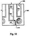
- Figure 10 is an enlarged view showing baffles lined with an insulator, adjacent pairs of the baffles defining shield pockets.
- the high density connector assembly includes a high density angled or right angle header 100 and a high density angled or right angle receptacle 200 for interconnecting a first circuit assembly, printed circuit or wiring board 22 and a second circuit assembly printed circuit or wiring board 24.
- the angled or right angle header 100 comprises an insulative housing 128, a plurality of conductive electrical contact elements 135 mounted in the housing 128 and at least one conductive shield 300.
- Figure 2 is an enlarged view of the first or front mating side 148 of the the high density angled or right angle header 100 of Figure 1.
- Figure 3 is an enlarged view of a top side 180 of the angled or right angle header 100 of Figures 1 and 2.
- the insulative housing 128 may have a base 142 and side walls 144 extending generally perpendicularly from the base 142.
- the base 142 and the side walls 144 partially enclose a contact region 146.
- a plurality of passages 184 arranged in rows and columns extend through the base 142.
- Figure 6 includes a cross sectional view of the header 100 connected to the receptacle 200 taken generally along the lines 6 in the direction of the arrows in Figures 3 and 5.
- Figure 7 includes a cross sectional view of the header 100 connected to the receptacle 200 taken generally along the lines 7 in the direction of the arrows in Figures 3 and 5.
- the conductive electrical contact elements 135 may have any configuration so long as they are useable as angled or right angle contact elements. In other words, they may be male elements, female elements to gender neutral. More specifically, as best seen in Figures 6 and 7, each one of the electrical contact elements 135 has a first connector contact or first contact portion 145 and a second connector contact or second contact portion 155.
- the first connector contacts 145 and the second connector connector contacts 155 are distal end portions of pins generally having a 0.635 mm (0.025 inches) by 0.635mm (0.025 inches) square cross section.
- Each of the contact elements 135 can have a first compliant or press-fit section 137 which forms an interference fit in one of the passages 184 to secure the contact elements 135 in the housing 128.
- the first connector contacts 145 are positioned in the contact region 146 for contacting one of the contacts (such as contacts 245) of a mating receptacle (such as receptacle 200). Note, however, the first connector contacts 145 of the high density header 100 are not limited to only connecting to the contacts 245 of the high density receptacle 200.
- the first connector contacts 145 of the high density header 100 can be adapted to connect to any plurality of terminals or contact elements with a plurality of first contacts arranged in rows and columns in a receptacle.
- the receptacle that is mateable with the header 100 can be a vertical receptacle or an angled or right angle receptacle.
- the contacts of the receptacle that is/are mateable with the header 100 are sockets or spring beams. If the receptacle that is mated with the header 100 is a right angle receptacle, then preferably it is the right angle receptacle 200 illustrated in Figure 1.
- the first connector contacts 145 are generally parallel to one another and arranged in rows and columns. There can be any number of rows and any number of columns of the first contacts 145. However, there are preferably at least two rows and at least two columns. Typically, there are three, four, five or six rows of the first connector contacts 145. The Figures depict four rows of the first connector contacts 145. Typically, there are many (e.g., up to 150) columns of the contact elements 135.
- Each one of the contact elements 135, except some of the contact elements 135 with their first connector contacts 145 in an nth row of the passages 184, has a middle portion 136 configured such that their second connector contacts 155 extend at an angle or perpendicularly with respect to their first connector contacts 145.
- these middle portions 136 have a right angle bend, two 45 degree angle bends or any shape that results in the second connector contacts 155 extending perpendicularly to the first connector contacts 145.
- the nth row is the fourth row which is an end row.
- a first set 188 of the contact elements 135 with their first connector contacts 145 in the nth row of the passages 184 have a middle portion 136 configured such that their second connector contacts 155 extend at an angle or perpendicularly to the first connector contacts 145.
- the first set 188 of the contact elements 135 in the fourth row are the longest contact elements 135 in the connector 100.
- the middle portions 136 of the first set 188 of the contact elements 135 in the nth row preferably have a right angle bend, two 45 degree angle bends or any shape that results in the second connector contacts 155 extending perpendicularly to the first connector contacts 145.
- the first set 188 comprises a plurality of the contact elements 135 in the nth row.
- the second set 190 comprises a plurality of the contact elements 135 in the nth row.
- the second connector contacts 155 of the second set 190 of the contact elements 135 are generally collinear or parallel to the first connector contacts 145.
- one of the second set 190 is between every pair of the first set 188.
- the second connector contacts 155, except those of the second set 190, can be through mount contacts or surface mount contacts.
- Figure 6 is a cross section showing one of the contact elements 135 in the second set 190.
- Figure 7 is a cross section showing one of the contact elements 135 in the first set 188.
- Each one of the conductive shields 300 is electrically connectable to a different subset of the second set 190, but none of the first set 188, of the contact elements 135.
- One or more or the shields 300 can be selectively placed over selected columns of the contact elements 135. While other columns of the contact elements 135 need not have a shield 300 associated with them depending on their intended use.
- the conductive shields 300 can be connected to the housing 128 by any means.
- each one of the second set 190 of the contact elements 135 can have a second compliant or press-fit section as its second contact 155 for forming an interference fit in a passage 305 in the shield 300 holding the shield 300 to the housing 128.
- FIG 8 is an isometric view of portions of one of the header shields 300 in accordance with the present invention.
- Each of the shields 300 includes a plurality of baffles 302.
- One of the baffles 302 is preferably for being positioned between and spaced from adjacent columns of the middle portions 136 of a group of the contact elements 135.
- the number in each group of the contact elements 135 may vary or be the same.
- each group of the contact elements 135 may comprise, for instance, 10 columns of the contact elements 135.
- one of the baffles 302 is for being placed between each pair of adjacent columns of the middle portions 136 of the contact elements 135 in the group, but this is not necessary.
- the baffles 302 include a first end baffle 303 which is for being positioned next to the last column of the middle portions 136 of the contact elements 135 in the group.
- the first end baffle 303 may be positioned between the last column of the middle portions 136 of the contact elements 135 in the group and a first column of the middle portions 136 of the contact elements 135 in a second adjacent group of the contact elements 135.
- the second group of the contact elements 135 may or may not have a corresponding shield 300 associated with it.
- the baffles 302 further include a second end baffle 304 which has a function similar to that of the first end baffle 303.
- the shields 300 including the baffles 302 can be made of any conductive non-magnetic material. Alternatively, the shields 300 and/or the baffles 302 can be polymeric and have a conductive layer or coating.
- each shield 300 includes a first shield contact 305 for contacting each of the second connector contacts 155 of the second set 190 of the contact elements 135.
- the first shield contacts 305 are slots, holes or passages in the shield 300 for receiving the second contacts or compliant sections 155 of the second set 190 of the contact elements 135.
- the shield 300 further includes a plurality of second shield contacts 315 positioned such that the second shield contacts 315 and the second connector contacts 155, excluding the second connector contacts 155 of the second set 190 of the contact elements 135 in the nth row, are arranged in rows and columns for connection to the circuit assembly 22.
- One of the second shield contacts 315 is shown in Figure 6.
- the second shield contacts 315 be arranged in one or more rows and in such row(s) with or without the second connector contacts 155 (excluding the second connector contacts 155 of the second set 190 of the contact elements 135 in the nth row) positioned in the row(s) with the second shield contacts 315.
- the second shield contacts 315 are end portions of pins.
- the shape of the second shield contacts 315 is different to that of, the second connector contacts 155.
- Both the second connector contacts 155 and the second shield contacts 315 can be pins but the cross section of one of them, such as the second shield contacts 315 can be larger than the cross section of the other.
- the second shield contacts 315 can be cast out of the same metal as the rest of the shield 300.
- the second shield contacts 315 can be end portions of conductive pins with a compliant or press-fit section 316 secured in holes or passages 317 in the shield 300.
- ground contacts 305 are provided to mate with one contact 155 in every other column of the contact elements 135. Since 4 contact elements 135 are depicted in each column of the contact elements 135, this provides 1 ground for each 7 signal paths.
- the shield can be configured to provide 1 ground path for every 11 signal paths.
- ground contacts 305 are provided to mate with one contact 155 in every third column of the contact elements 135.
- ground contacts 305 can be provided to mate with one contact 155 in every column of the contact elements 135 or with one or more contacts in any set or subset of the columns of the contact elements.
- each shield 300 further comprises a first elongated outer side wall 310 connected to each of the baffles 302.
- the compliant or press-fit sections 316 of the pins with the second shield contacts 315 are received in passages 317 in the first side wall 310.
- Each shield 300 further comprises a second elongated outer side wall 312 connected to each of the baffles 302.
- the second compliant or press-fit sections 155 i.e., the second connector contacts 155 of the second set 190 of the contact elements 135 in the nth row
- An outer surface of the second side wall 312 is generally perpendicular to an outer surface of the first side wall 310.
- a tab portion 311 of the first side wall 310 and/or a tab portion 313 of the second side wall 312 can extend past the end baffle 304 distal to end baffle 303 of the shield 300.
- the tab portions 311,313 are adapted to extend over a column of the contact elements 135 between a first end baffle 303 of a first one of the shields 300 and a second end baffle 304 of a second one of the shields 300. This is best seen in Figure 3.
- the tab portions 311,313 provide improved electrical and mechanical protection to the column of the contact elements 135 between the first end baffle 303 of a first one of the shields 300 and the second end baffle 304 of a second one of the shields 300.
- a minimum spacing is preferably provided between adjacent shields 300 to allow for manufacturing tolerance accumulation and differential thermal expansion between the metallic shields 300 and the plastic housings 128.
- the first elongated outer side wall 310, the second elongated outer side wall 312 and adjacent pairs of the baffles 302 define pockets 308 for receiving the middle portions 136 of one column of the contact elements 135.
- the pockets 308 can be coated with an insulative layer 309.
- Figure 10 is a view of a portion of the shield 300 illustrating the insulative layers 309. The portion of the shield shown in Figure 10 is an enlarged view of the portion of the shield 300 enclosed by phantom line segments 10 in Figure 8.
- Cleaning slots or passages 314 may exist through the shield 300 between the first side wall 310 and the second side wall 312 extending into each of the pockets 308. Further, the shields 300 may have stand-offs 320 along edges of the walls 310,312 and the baffles 302 to allow cleaning fluids to flow between the shield 300 and adjacent parts.
- the angled or right angle header 100 may further include an insulative spacer 350 associated with each one of the shields 300.
- the contact elements 135 may be rigid enough (and/or the handling and insertion to board may be gentle enough) not to use insulative spacers 350.
- Each one of the spacers 350 has a plurality of holes 352 through it arranged in rows and columns.
- the second connector contacts 155 except the second connector contacts 155 in the second set 190, extend through holes 352 of the spacers 350.
- the second shield contacts 315 extend through holes 352 of the spacers 350.
- the first row of the contact elements 135 do not pass through holes 352 in the spacers 350 because the first row of the contact elements 135 is the shortest, the strongest and the most difficult row to be inserted through holes of a spacer.
- each of the groups of the contact elements 135, except a first row of the contact elements and the second set 190 of the nth row of the contact elements 135 in that group extend through the holes 352 of a different one of the insulative spacers 350 such that the second shield contacts 315 and the second connector contacts 155, excluding the second contacts of the second set 190 of the contact elements 135 in the nth row, are on one side of the spacers 350 and the middle portions 136 are on another side of the spacers 350.
- the spacer 350 can have standoffs 354 to provide a space for cleaning purposes between the majority of the spacer 350 and the assembly 22.
- the spacer 350 can have sleeves (not depicted) extending from the holes 352 for insertion into the pockets 308 to reduce lateral movement of the spacer 350 and the second connector contacts 155 with respect to the shield 300.
- spacer 350 can be press fit on the second shield contacts 315 and/or the the second connector contacts 155, excluding the second contacts of the second set 190 of the contact elements 135 in the nth row.
- the angled or right angle connector 200 is structurally and functionally similar to the above described angled or right angle header 100, except the connector 200 is a receptacle. Parts of the receptacle 200 that correspond to or with parts in the header 100 are designated by the same numbers used in referring to the header parts increased by 100.
- the angled or right angle receptacle 200 comprises an insulative housing 228, a plurality of conductive electrical contact elements 235 mounted in the housing 228 and at least one conductive shield 400.
- Figure 4 is an enlarged view of a front or first, header or shroud, mating side or surface 248 of the high density angled or right angle receptacle 200 of Figure 1.
- Figure 5 is an enlarged view of a top side 280 of the angled or right angle receptacle 200 of Figures 1 and 4.
- the housing 228 has a plurality of passages 284 arranged in rows and columns extending perpendicularly from the first mating side or surface 248 through the housing 228.
- the conductive electrical contact elements 235 may have any configuration so long as they are useable as angled or right angle contact elements. In other words, they may be male elements, female elements or gender neutral. More specifically, as best seen in Figures 6 and 7, each one of the conductive electrical contact elements 235 has a first connector contact or first contact portion 245 and a second connector contact or second contact portion 255.
- the first connector contacts 245 can be, for instance, socket shaped or spring beams.
- the second connector contacts 255 can be substantially flat solder tails.
- One of the first connector contacts 245 is secured in each one of the passages 284 for contacting one of the contacts (such as contacts 145) of a mating header (such as header 100).
- first connector contacts 245 of the high density receptacle 200 are not limited to only connecting to the contacts 145 of the high density header 100.
- the first connector contacts 245 of the high density receptacle 200 can be adapted to connect to any plurality of terminals or contact elements with a plurality of first contacts arranged in rows and columns in a header.
- the header that is mateable with the receptacle 200 can be a vertical header or an angled or right angle header.
- the contacts of the header that is/are mateable with the receptacle 200 are end portions of pins. If the header that is mated with the receptacle 200 is a right angle header, then preferably it is the right angle header 100 illustrated in Figure 1.
- the first connector contacts 245 are generally parallel to one another and arranged in rows and columns in the passages 284. There can be any number of rows and any number of columns of the first connector contacts 245. However, there are preferably at least two rows and at least two columns. Typically, there are three, four, five or six rows of the first connector contacts 245. The Figures depict four rows of the first connector contacts 245. Typically, there are many columns (e.g., up to 150) of the first connector contacts 245.
- Each one of the contact elements 235 except some of the contact elements 235 with their first connector contacts 245 in an nth row of the passages 284, has a middle portion 236 configured such that their second connector contacts 255 extend at an angle or perpendicularly with respect to the first connector contacts 245.
- these middle portions 236 have a right angle bend, two 45 degree angle bends or any shape that results in the second connector contacts 255 extending perpendicularly to the first connector contacts 245.
- the nth row is the fourth row which is an end row.
- a first set 288 of the contact elements 235 with their first connector contacts 245 in the nth row of the passages 284 have a middle portion 236 configured such that their second connector contacts 255 extend at an angle or perpendicularly to the first connector contacts 245.
- the first set 288 of the contact elements 235 in the fourth row are the longest contact elements 235 in the connector 200.
- the middle portions 236 of the first set 288 of the contact elements 235 in the nth row preferably have a right angle bend, two 45 degree angle bends or any shape that results in the second connector contacts 255 extending perpendicularly to the first connector contacts 245.
- the first set 288 comprises a plurality of the contact elements 235 in the nth row.
- the second set 290 comprises a plurality of the contact elements 235 in the nth row.
- the second connector contacts 255 of the second set 290 of the contact elements 235 are generally collinear or parallel to the first connector contacts 245.
- one of the second set 290 is between every pair of the first set 288.
- the second connector contacts 255, except those of the second set 290, can be through mount contacts or surface mount contacts.
- Figure 6 is a cross section showing one of the contact elements 235 in the second set 290.
- Figure 7 is a cross section showing one of the contact elements 235 in the first set 288.
- Each one of the conductive shields 400 is electrically connectable to a different subset of the second set 290, but none of the first set 288, of the contact elements 235.
- the conductive shields 400 can be connected to the housing 228 by any means.
- each one of the second set 290 of the contact elements 235 can have an embossed section as its second contact 255 for forming an interference fit in a slot 405 in the shield 400 holding the shield 400 to the housing 228.
- the shield 400 may further have projections or teeth 406 that fit in corresponding slots 229 in or dividing a step on the housing 228.
- the projections 406 can be slightly larger than the slots forming a tight or interference fit between the projections 406 and the slots 229 further securing the shield 400 to the housing 228.
- the shield 400 may further have fingers (in addition to or in lieu of the projections 406) that snap fit over a ridge (in addition to or in lieu of the segmented ridge defining the slots 229) on the housing 228.
- FIG 9 is an isometric view of portions of one of the receptacle shields 400 in accordance with the present invention.
- Each of the shields 400 includes a plurality of baffles 402.
- One of the baffles 402 is preferably for being positioned between and spaced from adjacent columns of the middle portions 236 of a group of the contact elements 235.
- the number in each group of the contact elements 235 may vary or be the same.
- each group of the contact elements 235 may comprise, for instance, 10 columns of the contact elements 235.
- one of the baffles 402 is for being placed between each pair of adjacent columns of the middle portions 236 of the contact elements 235 in the group, but this is not necessary.
- the baffles 402 include a first end baffle 403 which is for being positioned next to the last column of the middle portions 236 of the contact elements 235 in the group.
- the first end baffle 403 may be positioned between the last column of the middle portions 236 of the contact elements 235 in the group and a first column of the middle portions 236 of the contact elements 235 in another adjacent group of the contact elements 235.
- the baffles 402 further include a second end baffle 404 which has a function similar to that of the first end baffle 403.
- the shields 400 including the baffles 402 can be made of any conductive material. Alternatively, the shields 400 and/or the baffles 402 can be polymeric and have a conductive layer or coating.
- each shield 400 includes a first shield contact 405 for contacting each of the second connector contacts 255 of the second set 290 of the contact elements 235.
- the first shield contact 405 is a slot in the shield 400 running generally transverse to the baffles 402 for receiving the second contacts or embossed sections 255 of the second set 290 of the contact elements 235.
- the shield 400 further includes a plurality of second shield contacts 415 positioned such that the second shield contacts 415 and the second connector contacts 255, excluding the second connector contacts 255 of the second set 290 of the contact elements 235 in the nth row, are arranged in rows and columns for connection to the circuit assembly 24.
- One of the second shield contacts 415 is shown in Figure 6.
- the second shield contacts 415 be arranged in one or more rows and in such row(s) with or without the second connector contacts 255 (excluding the second connector contacts 255 of the second set 290 of the contact elements 235 in the nth row) positioned in the row(s) with the second shield contacts 415.
- the second shield contacts 415 are end portions of pins.
- the Shape of the second shield contacts 415 is, a different shape to that of the second connector contacts 255.
- Both the second connector contacts 255 and the second shield contacts 415 can be pins, but the cross section of one of them, such as the second shield contacts 415 can be larger than the cross section of the other.
- the second shield contacts 415 can be cast out of the same metal as the rest of the shield 400.
- the second shield contacts 415 can be end portions of conductive pins with a compliant or press-fit section 416 secured in holes or passages 417 in the shield 400.
- each shield 400 further comprises a first elongated outer side wall 410 connected to each of the baffles 402.
- the compliant or press-fit sections 416 of the pins with the second shield contacts 415 are received in passages 417 in the first side wall 410.
- Each shield 400 further comprises a second elongated outer side wall 412 connected to each of the baffles 402.
- the second embossed sections 255 i.e., the second connector contacts 255 of the second set 290 of the contact elements 235 in the nth row
- An outer surface of the second side wall 412 is generally perpendicular to an outer surface of the first side wall 410.
- a tab portion 411 of the first side wall 410 and/or a tab portion 413 of the second side wall 412 can extend past the end baffle 404 distal to end baffle 403 of the shield 400.
- the tab portions 411,413 are adapted to extend over a column of the contact elements 235 between a first end baffle 403 of a first one of the shields 400 and a second end baffle 404 of a second one of the shields 400. This is best seen in Figure 5.
- the first elongated outer side wall 410, the second elongated outer side wall 412 and adjacent pairs of the baffles 402 define pockets 408 for receiving the middle portions 236 of one column of the contact elements 235.
- the pockets 408 can be coated with an insulative layer, like layers 309 illustrated in Figure 10.
- Cleaning slots or passages 414 may exist through the shield 400 between the first side wall 410 and the second side wall 412 extending into each of the pockets 408. Further, the shields 400 may have stand-offs 420 along edges of the walls 410,412 and the baffles 402 to allow cleaning fluids to flow between the shield 400 and adjacent parts.
- the angled or right angle receptacle 200 may further include an insulative spacer 450 associated with each one of the shields 400.
- the insulative spacers 450 may be the same as the insulative spacers 350.
- Holes 452 through the spacers 450 may be of different size or shape than the holes 352 in the spacer 350.
- the first and second circuit assemblies 22, 24 can be any assemblies that include a plurality of conductors, leads, plated through holes or conductive paths, pads or areas 26. Each or either one of the circuit assemblies 22, 24 can be a printed wiring board or a printed circuit board, such as a backpanel, a mother board or a daughter board. Each or either one of the circuit assemblies 22, 24 can be a cable assembly.
- the circuit assemblies 22, 24 can be rigid or flexible.
- the conductive U-shaped structures disclosed in U.S. Patent 4,898,546 can be used in combination with the present invention to connect any of the contact elements 135, 235 to the shields 300, 400 and, thus, to ground, including any of the contact elements 135, 235 that are not in the nth row.
- one or more of the U-shaped structures can be used as disclosed in U.S. Patent 4,898,546.
- the U-shaped structures instead of securing the U-shaped structures in an insulative comb-like member, the U-shaped structures can be secured in the pockets 308 of the conductive shields 300, 400.
- ground structures or shields of the present invention can be modified to be used on any angled receptacle or header where the two contacts of the contact elements of the receptacle or header are at an angle other than 180 degrees from one another.
- the insulative housings can be made of various plastics, such as polyetherimide resin or polyphenylene sulfide resin.
- the conductive walls, conductive bases, baffles and shields can be made of any nonmagnetic metal or metal alloy including zinc, aluminum, copper, brass or alloys thereof.
- the contact elements of the present invention can be made from any suitable metal used for electrical terminals, such as brass, phosphor bronze, beryllium copper and the like.
- the contact elements may be plated or coated with a conductive layer, such as tin, nickel, palladium, gold, silver or a suitable alloy.
Landscapes
- Details Of Connecting Devices For Male And Female Coupling (AREA)
- Coupling Device And Connection With Printed Circuit (AREA)
Description
- This invention relates to electrical connectors with a ground structure for cross talk control between signal carrying conductors and, in particular, where the connector is a right angle receptacle or a right angle header.
- With the advance of technology, a high density of electronic circuits and components can be located on a printed wiring board or printed circuit board (PCB). Along with this miniaturization of electronic circuits and components, electrical connectors are needed to electrically and mechanically interconnect one PCB, such as a back panel or mother board, to one or more other PCBs, such as daughter boards. Further, it is typically desirable for such connectors to have a high signal density capacity. That is, the connectors should permit a high number of signals to pass through the connector per unit volume of the connector. However, electrical signals carried on a conductor can interfere with a signal carried on an adjacent conductor.
- This interfering electrical effect that an electrical signal carried on a given conductor exerts on a signal carried on an adjacent conductor is referred to as "cross talk." Controlling this cross talk is especially important in high density connectors. Such control can be implemented in a variety of ways.
- One method of controlling cross talk is to connect certain terminals in a high density connector to conductive areas of a printed circuit board that are in turn grounded or connected to a predetermined ground potential. This solution is external to the connector.
- U.S. Patents 4,655,518 (to Lennart B. Johnson et al.), 4686,607 (to Lennart B. Johnson) and 4,869,677 (to Lennart B. Johnson et al.) disclose a daughter board/backplane assembly with contact elements dedicated for grounding purposes. Header contact elements have contacts that can be connected to ground or a predetermined potential on a backplane. The header contact elements have other spring contacts carried by an inside header wall for touching contacts carried by a right angle receptacle outer wall. Other contacts are integral with and perpendicular to the contacts carried by the right angle receptacle outer wall for connection to the daughter board.
- U.S. Patent 4,601,527 issued to Timothy A. Lemke discloses an internal shielding structure for connectors, specifically in vertical and right angle headers. The shielding structure includes a ground strip affixed to a mating surface of a header housing. The shielding structure further includes an elongated conductive spring contact with contact beams that extend in holes of side walls of the housing, lock tabs that connect to the ground strip and ground bars for connection to a grounded chassis.
- U.S. Patent 4,824,383 issued to Timothy A. Lemke discloses a shielding structure in connectors or plug-type terminators for either a multiple conductor cable or a multiple tracing substrate that electrically isolates individual or groups of contact elements in the terminator to prevent or minimize cross talk between adjacent conductors and to prevent or minimize degradation of signal transmission. The terminator includes a ground structure with generally U-shaped channels. Contact elements extend into the channels. The ground structure is connected to a predetermined potential, rather than dedicating some of the contact elements for this purpose.
- U.S.-A-4,898,546 discloses ground shield devices for right angle connectors. A different one of the shield devices straddles alternate columns of contact elements in the connector. Each shield device clips to a tail of one of the contact elements straddled by the shield device. The shield devices are connected to ground or a predetermined potential.
- It is an object of this invention to provide an improved high density electrical connector for electrically and mechanically interconnecting electronic circuits and/or components controlling cross talk within the connector.
- According to one aspect of the present invention there is provided an angled or right angle electrical connector for electrically and mechanically inter-connecting a circuit assembly to another complementary connector, the angled or right angle connector comprising:
- an insulative housing;
- a plurality of electrical contact elements at least partly in the housing each one of the contact elements having a first contact portion and a second contact portion,
- and at least one conductive shield;
- wherein the first contact portions of the elements are arranged in rows and columns to contact corresponding terminal contacts of a plurality of terminals arranged in similar rows and columns of said other complementary connector;
- each one of the contact elements except for some of the contact elements with their first contact portions in an nth row, includes a middle portion configured such that the second contact portions thereof extend at an angle with respect to the first contact portions:
- and wherein there are a first set and a second set of the plurality of the contact elements with their first contact portions in the nth row, each element in the first set having a middle portion configured such that its second contact portion extends at the angle with respect to the first contact portion and each contact element in the second set of the plurality of the contact elements being different in shape than the first set and said at least one conductive shield is electrically connected to the second set or a subset of the second set but none of the first set of the contact elements.
- The connector may comprise a plurality of conductive shields each of the shields being electrically connected to a subset of the second set but none of the first set of the contact elements with their first contact portions in the nth row.
- In another aspect of the invention the connector is in the form of a receptacle for electrically and mechanically inter-connecting a circuit assembly to a header or shroud, the receptacle comprising:
- an insulative housing having a first, header or shroud, mating surface and a plurality of passages arranged in rows and columns extending perpendicularly from the first mating surface through the housing;
- a plurality of electrical contact elements at least partially in the housing;
- each one of the contact elements having a first contact portion and a second contact portion;
- and at least one conductive shield;
- wherein one of the first contact portions is positioned in an associated one of the passages to contact corresponding terminal contacts of a plurality of terminals arranged in similar rows and columns in the said header;
- each one of the contact elements except for some of the contact elements with their first contact portion in an nth row of the passages include a middle portion configured such that the second contact portion thereof extends at an angle with respect to the first contact portion,
- and wherein there are a first set and a second set of the plurality of the contact elements with their first contact portions in the nth row of the passages each contact element in the first set having a middle portion configured such that its second contact portion extends at the angle with respect to the first contact portion and
- each contact element in the second set of the plurality of the contact elements being different in shape than the first set
- and said conductive shield is electrically connected to the second set or a subset of the second set but none of the first set of the contact elements.
- In a further aspect of the invention the connector is in the form of a header for electrically and mechanically inter-connecting a circuit assembly to a receptacle the header comprising:
- an insulative housing having a base and side walls the base and the side walls partially enclosing a contact region the base having a plurality of passages arranged in rows and columns extending through the base;
- a plurality of electrical contact elements at least partially in the housing;
- each one of the contact elements having a first contact portion and a second contact portion,
- and at least one conductive shield;
- wherein one of the contact elements extends through and is fixed in an associated one of the passages with the first contact portion positioned in the contact region to contact corresponding terminal contacts of a plurality of terminals arranged in similar rows and columns in the said receptacle ;
- each one of the contact elements except for some of the contact elements with their first contact portion in an nth row of the passages include a middle portion configured such that the second contact portion thereof extends at an angle with respect to the first contact portion,
- and wherein there are a first set and a second set of the plurality of the contact elements with their first contact portions in the nth row of the passages each contact element in the first set having a middle portion configured such that its second contact portion extends at the angle with respect to the first contact portion, and
- each contact element in the second set of the plurality of the contact elements being different in shape than the first set,
- and said at least one conductive shield is electrically connected to the second set or a subset of the second set but none of the first set of the contact elements.
- In a preferred embodiment of the connector, the shield or shields may comprise baffles positioned between and spaced from columns of the middle portions of a group of the contact elements;
- a first shield contact for contacting each of the second contact portions of the second set but not the second contact portions of the first set in the group of the contact elements and
- a plurality of the second shield contacts positioned such that the second contact portions excluding the second contact portions of the second set of the contact elements in the nth row, and the second shield contacts are arranged in rows and columns for connection to the circuit assembly.
- Ideally, the contact elements of the connector having their first contact portions in the nth row and belonging to the second set of the elements have no middle portions.
- In a further aspect of the present invention a conductive shield is provided for use with an angled or right angle connector, the shield serving to reduce cross-talk and comprising:
- a plurality of baffles
- a plurality of first shield contacts
- a plurality of second shield contacts
- a first elongated outer side wall connected to each of the baffles, the first outer side wall having an outer surface;
- a second elongated outer side wall connected to each of the baffles the second side wall having an outer surface generally perpendicular to the outer surface of the first side wall
- each of the plurality of baffles being disposed for positioning between and spaced from adjacent columns of the middle portions of the contact elements of the connector
- one of the first shield contacts being connectable with each of the second contact portions of the subset of the second set but none of the first set of the contact elements in the nth row,
- the plurality of the second shield contacts being disposed for arrangement together with the second contact portion of the first set but not the second set of the contact elements in the nth row, in rows and columns that are at an angle with respect to the rows and columns of the first contact portions.
- The invention can be more fully understood from the following detailed description thereof in connection with accompanying drawings which form a part of this application and which:
- Figure 1 is an exploded perspective view of a high density connector assembly in accordance with the present invention, the assembly including a high density angled or right angle receptacle and a high density angled or right angle header for interconnecting a first printed circuit or wiring board and a second printed circuit or wiring board.
- Figure 2 is an enlarged view of a front or first mating side of the the high density angled or right angle header of Figure 1.
- Figure 3 is an enlarged view of a top side of the angled or right angle header of Figures 1 and 2.
- Figure 4 is an enlarged view of a front or first mating side of the high density angled or right angle receptacle of Figure 1.
- Figure 5 is an enlarged view of a top side of the angled or right angle receptacle of Figures 1 and 4.
- Figure 6 is a first sectional view of the angled or right angle header of Figures 1-3 connected to the angled or right angle receptacle of Figures 1, 4 and 5.
- Figure 7 is a second sectional view of the angled or right angle header of Figures 1-3 connected to the angled or right angle receptacle of Figures 1, 4 and 5.
- Figure 8 is an isometric view of a header shield in accordance with the present invention.
- Figure 9 is an isometric view of a receptacle shield in accordance with the present invention.
- Figure 10 is an enlarged view showing baffles lined with an insulator, adjacent pairs of the baffles defining shield pockets.
- Throughout the following detailed description, similar reference characters refer to similar elements in all figures of the drawings.
- Referring to Figure 1, there is illustrated a high density connector assembly in accordance with the present invention. The high density connector assembly includes a high density angled or
right angle header 100 and a high density angled orright angle receptacle 200 for interconnecting a first circuit assembly, printed circuit or wiringboard 22 and a second circuit assembly printed circuit or wiringboard 24. - The angled or
right angle header 100 comprises aninsulative housing 128, a plurality of conductiveelectrical contact elements 135 mounted in thehousing 128 and at least oneconductive shield 300. Figure 2 is an enlarged view of the first orfront mating side 148 of the the high density angled orright angle header 100 of Figure 1. Figure 3 is an enlarged view of atop side 180 of the angled orright angle header 100 of Figures 1 and 2. - Referring back to Figure 1, the
insulative housing 128 may have a base 142 andside walls 144 extending generally perpendicularly from thebase 142. Thebase 142 and theside walls 144 partially enclose acontact region 146. As best seen in Figures 6 and 7, a plurality ofpassages 184 arranged in rows and columns extend through thebase 142. Figure 6 includes a cross sectional view of theheader 100 connected to thereceptacle 200 taken generally along thelines 6 in the direction of the arrows in Figures 3 and 5. Figure 7 includes a cross sectional view of theheader 100 connected to thereceptacle 200 taken generally along thelines 7 in the direction of the arrows in Figures 3 and 5. - Referring to Figure 1, the conductive
electrical contact elements 135 may have any configuration so long as they are useable as angled or right angle contact elements. In other words, they may be male elements, female elements to gender neutral. More specifically, as best seen in Figures 6 and 7, each one of theelectrical contact elements 135 has a first connector contact orfirst contact portion 145 and a second connector contact orsecond contact portion 155. Preferably, thefirst connector contacts 145 and the secondconnector connector contacts 155 are distal end portions of pins generally having a 0.635 mm (0.025 inches) by 0.635mm (0.025 inches) square cross section. Each of thecontact elements 135 can have a first compliant or press-fit section 137 which forms an interference fit in one of thepassages 184 to secure thecontact elements 135 in thehousing 128. Thefirst connector contacts 145 are positioned in thecontact region 146 for contacting one of the contacts (such as contacts 245) of a mating receptacle (such as receptacle 200). Note, however, thefirst connector contacts 145 of thehigh density header 100 are not limited to only connecting to thecontacts 245 of thehigh density receptacle 200. Thefirst connector contacts 145 of thehigh density header 100 can be adapted to connect to any plurality of terminals or contact elements with a plurality of first contacts arranged in rows and columns in a receptacle. The receptacle that is mateable with theheader 100 can be a vertical receptacle or an angled or right angle receptacle. Preferably, the contacts of the receptacle that is/are mateable with theheader 100 are sockets or spring beams. If the receptacle that is mated with theheader 100 is a right angle receptacle, then preferably it is theright angle receptacle 200 illustrated in Figure 1. - The
first connector contacts 145 are generally parallel to one another and arranged in rows and columns. There can be any number of rows and any number of columns of thefirst contacts 145. However, there are preferably at least two rows and at least two columns. Typically, there are three, four, five or six rows of thefirst connector contacts 145. The Figures depict four rows of thefirst connector contacts 145. Typically, there are many (e.g., up to 150) columns of thecontact elements 135. - Each one of the
contact elements 135, except some of thecontact elements 135 with theirfirst connector contacts 145 in an nth row of thepassages 184, has amiddle portion 136 configured such that theirsecond connector contacts 155 extend at an angle or perpendicularly with respect to theirfirst connector contacts 145. Preferably, thesemiddle portions 136 have a right angle bend, two 45 degree angle bends or any shape that results in thesecond connector contacts 155 extending perpendicularly to thefirst connector contacts 145. In the embodiment illustrated in Figures 1-3, the nth row is the fourth row which is an end row. Referring to Figure 1, afirst set 188 of thecontact elements 135 with theirfirst connector contacts 145 in the nth row of thepassages 184 have amiddle portion 136 configured such that theirsecond connector contacts 155 extend at an angle or perpendicularly to thefirst connector contacts 145. Preferably, thefirst set 188 of thecontact elements 135 in the fourth row are thelongest contact elements 135 in theconnector 100. Like themiddle portions 136 of thecontact elements 135 in the rows other than the nth row, themiddle portions 136 of thefirst set 188 of thecontact elements 135 in the nth row preferably have a right angle bend, two 45 degree angle bends or any shape that results in thesecond connector contacts 155 extending perpendicularly to thefirst connector contacts 145. There is also asecond set 190 of at least one of thecontact elements 135 with its/theirfirst connector contacts 145 in the nth row of thepassages 184. Preferably, thefirst set 188 comprises a plurality of thecontact elements 135 in the nth row. Preferably, thesecond set 190 comprises a plurality of thecontact elements 135 in the nth row. More preferably, thesecond connector contacts 155 of thesecond set 190 of thecontact elements 135 are generally collinear or parallel to thefirst connector contacts 145. Also more preferably, one of thesecond set 190 is between every pair of thefirst set 188. Thesecond connector contacts 155, except those of thesecond set 190, can be through mount contacts or surface mount contacts. Figure 6 is a cross section showing one of thecontact elements 135 in thesecond set 190. Figure 7 is a cross section showing one of thecontact elements 135 in thefirst set 188. - Each one of the
conductive shields 300 is electrically connectable to a different subset of thesecond set 190, but none of thefirst set 188, of thecontact elements 135. One or more or theshields 300 can be selectively placed over selected columns of thecontact elements 135. While other columns of thecontact elements 135 need not have ashield 300 associated with them depending on their intended use. Theconductive shields 300 can be connected to thehousing 128 by any means. For instance, each one of thesecond set 190 of thecontact elements 135 can have a second compliant or press-fit section as itssecond contact 155 for forming an interference fit in apassage 305 in theshield 300 holding theshield 300 to thehousing 128. - Figure 8 is an isometric view of portions of one of the header shields 300 in accordance with the present invention. Each of the
shields 300 includes a plurality ofbaffles 302. One of thebaffles 302 is preferably for being positioned between and spaced from adjacent columns of themiddle portions 136 of a group of thecontact elements 135. The number in each group of thecontact elements 135 may vary or be the same. As illustrated in the Figures, each group of thecontact elements 135 may comprise, for instance, 10 columns of thecontact elements 135. Preferably, one of thebaffles 302 is for being placed between each pair of adjacent columns of themiddle portions 136 of thecontact elements 135 in the group, but this is not necessary. Preferably, thebaffles 302 include afirst end baffle 303 which is for being positioned next to the last column of themiddle portions 136 of thecontact elements 135 in the group. Thefirst end baffle 303 may be positioned between the last column of themiddle portions 136 of thecontact elements 135 in the group and a first column of themiddle portions 136 of thecontact elements 135 in a second adjacent group of thecontact elements 135. The second group of thecontact elements 135 may or may not have acorresponding shield 300 associated with it. Thebaffles 302 further include asecond end baffle 304 which has a function similar to that of thefirst end baffle 303. Theshields 300 including thebaffles 302 can be made of any conductive non-magnetic material. Alternatively, theshields 300 and/or thebaffles 302 can be polymeric and have a conductive layer or coating. - Referring to Figures 6 and 8, each
shield 300 includes afirst shield contact 305 for contacting each of thesecond connector contacts 155 of thesecond set 190 of thecontact elements 135. Preferably, thefirst shield contacts 305 are slots, holes or passages in theshield 300 for receiving the second contacts orcompliant sections 155 of thesecond set 190 of thecontact elements 135. Theshield 300 further includes a plurality ofsecond shield contacts 315 positioned such that thesecond shield contacts 315 and thesecond connector contacts 155, excluding thesecond connector contacts 155 of thesecond set 190 of thecontact elements 135 in the nth row, are arranged in rows and columns for connection to thecircuit assembly 22. One of thesecond shield contacts 315 is shown in Figure 6. It is within the scope of this invention for thesecond shield contacts 315 to be arranged in one or more rows and in such row(s) with or without the second connector contacts 155 (excluding thesecond connector contacts 155 of thesecond set 190 of thecontact elements 135 in the nth row) positioned in the row(s) with thesecond shield contacts 315. Preferably, thesecond shield contacts 315 are end portions of pins. As shown the shape of thesecond shield contacts 315 is different to that of, thesecond connector contacts 155. Both thesecond connector contacts 155 and thesecond shield contacts 315 can be pins but the cross section of one of them, such as thesecond shield contacts 315 can be larger than the cross section of the other. Thesecond shield contacts 315 can be cast out of the same metal as the rest of theshield 300. Alternatively, thesecond shield contacts 315 can be end portions of conductive pins with a compliant or press-fit section 316 secured in holes orpassages 317 in theshield 300. - The
shield 300 illustrated in the figures provides 1 ground path for every 7 signal paths. In other words,ground contacts 305 are provided to mate with onecontact 155 in every other column of thecontact elements 135. Since 4contact elements 135 are depicted in each column of thecontact elements 135, this provides 1 ground for each 7 signal paths. Alternatively, the shield can be configured to provide 1 ground path for every 11 signal paths. In this case,ground contacts 305 are provided to mate with onecontact 155 in every third column of thecontact elements 135. Alternatively,ground contacts 305 can be provided to mate with onecontact 155 in every column of thecontact elements 135 or with one or more contacts in any set or subset of the columns of the contact elements. - Preferably, each
shield 300 further comprises a first elongatedouter side wall 310 connected to each of thebaffles 302. The compliant or press-fit sections 316 of the pins with thesecond shield contacts 315 are received inpassages 317 in thefirst side wall 310. Eachshield 300 further comprises a second elongatedouter side wall 312 connected to each of thebaffles 302. The second compliant or press-fit sections 155 (i.e., thesecond connector contacts 155 of thesecond set 190 of thecontact elements 135 in the nth row) are received in thepassages 305 in thesecond side wall 312. An outer surface of thesecond side wall 312 is generally perpendicular to an outer surface of thefirst side wall 310. Atab portion 311 of thefirst side wall 310 and/or atab portion 313 of thesecond side wall 312 can extend past theend baffle 304 distal to endbaffle 303 of theshield 300. The tab portions 311,313 are adapted to extend over a column of thecontact elements 135 between afirst end baffle 303 of a first one of theshields 300 and asecond end baffle 304 of a second one of theshields 300. This is best seen in Figure 3. The tab portions 311,313 provide improved electrical and mechanical protection to the column of thecontact elements 135 between thefirst end baffle 303 of a first one of theshields 300 and thesecond end baffle 304 of a second one of theshields 300. A minimum spacing is preferably provided betweenadjacent shields 300 to allow for manufacturing tolerance accumulation and differential thermal expansion between themetallic shields 300 and theplastic housings 128. - The first elongated
outer side wall 310, the second elongatedouter side wall 312 and adjacent pairs of thebaffles 302 definepockets 308 for receiving themiddle portions 136 of one column of thecontact elements 135. To ensure that themiddle portions 136 do not short out by contacting a conductive portion of theshield 300, thepockets 308 can be coated with aninsulative layer 309. Figure 10 is a view of a portion of theshield 300 illustrating the insulative layers 309. The portion of the shield shown in Figure 10 is an enlarged view of the portion of theshield 300 enclosed byphantom line segments 10 in Figure 8. - Cleaning slots or
passages 314 may exist through theshield 300 between thefirst side wall 310 and thesecond side wall 312 extending into each of thepockets 308. Further, theshields 300 may have stand-offs 320 along edges of the walls 310,312 and thebaffles 302 to allow cleaning fluids to flow between theshield 300 and adjacent parts. - The angled or
right angle header 100 may further include aninsulative spacer 350 associated with each one of theshields 300. However, thecontact elements 135 may be rigid enough (and/or the handling and insertion to board may be gentle enough) not to useinsulative spacers 350. Each one of thespacers 350 has a plurality ofholes 352 through it arranged in rows and columns. Thesecond connector contacts 155, except thesecond connector contacts 155 in thesecond set 190, extend throughholes 352 of thespacers 350. Further, thesecond shield contacts 315 extend throughholes 352 of thespacers 350. Preferably, as best seen in Figures 6 and 7, the first row of thecontact elements 135 do not pass throughholes 352 in thespacers 350 because the first row of thecontact elements 135 is the shortest, the strongest and the most difficult row to be inserted through holes of a spacer. Restated, each of the groups of thecontact elements 135, except a first row of the contact elements and thesecond set 190 of the nth row of thecontact elements 135 in that group, extend through theholes 352 of a different one of theinsulative spacers 350 such that thesecond shield contacts 315 and thesecond connector contacts 155, excluding the second contacts of thesecond set 190 of thecontact elements 135 in the nth row, are on one side of thespacers 350 and themiddle portions 136 are on another side of thespacers 350. Thespacer 350 can havestandoffs 354 to provide a space for cleaning purposes between the majority of thespacer 350 and theassembly 22. Thespacer 350 can have sleeves (not depicted) extending from theholes 352 for insertion into thepockets 308 to reduce lateral movement of thespacer 350 and thesecond connector contacts 155 with respect to theshield 300. For attachment and location purposes,spacer 350 can be press fit on thesecond shield contacts 315 and/or the thesecond connector contacts 155, excluding the second contacts of thesecond set 190 of thecontact elements 135 in the nth row. - The angled or
right angle connector 200 is structurally and functionally similar to the above described angled orright angle header 100, except theconnector 200 is a receptacle. Parts of thereceptacle 200 that correspond to or with parts in theheader 100 are designated by the same numbers used in referring to the header parts increased by 100. - Referring to Figure 1, the angled or
right angle receptacle 200 comprises aninsulative housing 228, a plurality of conductiveelectrical contact elements 235 mounted in thehousing 228 and at least oneconductive shield 400. Figure 4 is an enlarged view of a front or first, header or shroud, mating side orsurface 248 of the high density angled orright angle receptacle 200 of Figure 1. Figure 5 is an enlarged view of atop side 280 of the angled orright angle receptacle 200 of Figures 1 and 4. - As best seen in Figures 6 and 7, the
housing 228 has a plurality ofpassages 284 arranged in rows and columns extending perpendicularly from the first mating side orsurface 248 through thehousing 228. - Referring to Figure 1, the conductive
electrical contact elements 235 may have any configuration so long as they are useable as angled or right angle contact elements. In other words, they may be male elements, female elements or gender neutral. More specifically, as best seen in Figures 6 and 7, each one of the conductiveelectrical contact elements 235 has a first connector contact orfirst contact portion 245 and a second connector contact orsecond contact portion 255. Thefirst connector contacts 245 can be, for instance, socket shaped or spring beams. Thesecond connector contacts 255 can be substantially flat solder tails. One of thefirst connector contacts 245 is secured in each one of thepassages 284 for contacting one of the contacts (such as contacts 145) of a mating header (such as header 100). Note, however, thefirst connector contacts 245 of thehigh density receptacle 200 are not limited to only connecting to thecontacts 145 of thehigh density header 100. Thefirst connector contacts 245 of thehigh density receptacle 200 can be adapted to connect to any plurality of terminals or contact elements with a plurality of first contacts arranged in rows and columns in a header. The header that is mateable with thereceptacle 200 can be a vertical header or an angled or right angle header. Preferably, the contacts of the header that is/are mateable with thereceptacle 200 are end portions of pins. If the header that is mated with thereceptacle 200 is a right angle header, then preferably it is theright angle header 100 illustrated in Figure 1. - The
first connector contacts 245 are generally parallel to one another and arranged in rows and columns in thepassages 284. There can be any number of rows and any number of columns of thefirst connector contacts 245. However, there are preferably at least two rows and at least two columns. Typically, there are three, four, five or six rows of thefirst connector contacts 245. The Figures depict four rows of thefirst connector contacts 245. Typically, there are many columns (e.g., up to 150) of thefirst connector contacts 245. - Each one of the
contact elements 235, except some of thecontact elements 235 with theirfirst connector contacts 245 in an nth row of thepassages 284, has amiddle portion 236 configured such that theirsecond connector contacts 255 extend at an angle or perpendicularly with respect to thefirst connector contacts 245. Preferably, thesemiddle portions 236 have a right angle bend, two 45 degree angle bends or any shape that results in thesecond connector contacts 255 extending perpendicularly to thefirst connector contacts 245. In the embodiment illustrated in Figures 1, 4 and 5, the nth row is the fourth row which is an end row. Referring to Figure 1, afirst set 288 of thecontact elements 235 with theirfirst connector contacts 245 in the nth row of thepassages 284 have amiddle portion 236 configured such that theirsecond connector contacts 255 extend at an angle or perpendicularly to thefirst connector contacts 245. Preferably, thefirst set 288 of thecontact elements 235 in the fourth row are thelongest contact elements 235 in theconnector 200. Like themiddle portions 236 of thecontact elements 235 in the rows other than the nth row, themiddle portions 236 of thefirst set 288 of thecontact elements 235 in the nth row preferably have a right angle bend, two 45 degree angle bends or any shape that results in thesecond connector contacts 255 extending perpendicularly to thefirst connector contacts 245. There is also asecond set 290 of at least one of thecontact elements 235 with its/theirfirst connector contacts 245 in the nth row of thepassages 284. Preferably, thefirst set 288 comprises a plurality of thecontact elements 235 in the nth row. Preferably, thesecond set 290 comprises a plurality of thecontact elements 235 in the nth row. More preferably, thesecond connector contacts 255 of thesecond set 290 of thecontact elements 235 are generally collinear or parallel to thefirst connector contacts 245. Also more preferably, one of thesecond set 290 is between every pair of thefirst set 288. Thesecond connector contacts 255, except those of thesecond set 290, can be through mount contacts or surface mount contacts. Figure 6 is a cross section showing one of thecontact elements 235 in thesecond set 290. Figure 7 is a cross section showing one of thecontact elements 235 in thefirst set 288. - Each one of the
conductive shields 400 is electrically connectable to a different subset of thesecond set 290, but none of thefirst set 288, of thecontact elements 235. Theconductive shields 400 can be connected to thehousing 228 by any means. For instance, each one of thesecond set 290 of thecontact elements 235 can have an embossed section as itssecond contact 255 for forming an interference fit in aslot 405 in theshield 400 holding theshield 400 to thehousing 228. Theshield 400 may further have projections orteeth 406 that fit in correspondingslots 229 in or dividing a step on thehousing 228. Theprojections 406 can be slightly larger than the slots forming a tight or interference fit between theprojections 406 and theslots 229 further securing theshield 400 to thehousing 228. Theshield 400 may further have fingers (in addition to or in lieu of the projections 406) that snap fit over a ridge (in addition to or in lieu of the segmented ridge defining the slots 229) on thehousing 228. - Figure 9 is an isometric view of portions of one of the receptacle shields 400 in accordance with the present invention. Each of the
shields 400 includes a plurality ofbaffles 402. One of thebaffles 402 is preferably for being positioned between and spaced from adjacent columns of themiddle portions 236 of a group of thecontact elements 235. The number in each group of thecontact elements 235 may vary or be the same. As illustrated in the Figures, each group of thecontact elements 235 may comprise, for instance, 10 columns of thecontact elements 235. Preferably, one of thebaffles 402 is for being placed between each pair of adjacent columns of themiddle portions 236 of thecontact elements 235 in the group, but this is not necessary. Preferably, thebaffles 402 include afirst end baffle 403 which is for being positioned next to the last column of themiddle portions 236 of thecontact elements 235 in the group. Thefirst end baffle 403 may be positioned between the last column of themiddle portions 236 of thecontact elements 235 in the group and a first column of themiddle portions 236 of thecontact elements 235 in another adjacent group of thecontact elements 235. Thebaffles 402 further include asecond end baffle 404 which has a function similar to that of thefirst end baffle 403. Theshields 400 including thebaffles 402 can be made of any conductive material. Alternatively, theshields 400 and/or thebaffles 402 can be polymeric and have a conductive layer or coating. - Referring to Figures 6 and 9, each
shield 400 includes afirst shield contact 405 for contacting each of thesecond connector contacts 255 of thesecond set 290 of thecontact elements 235. Preferably, thefirst shield contact 405 is a slot in theshield 400 running generally transverse to thebaffles 402 for receiving the second contacts or embossedsections 255 of thesecond set 290 of thecontact elements 235. Theshield 400 further includes a plurality ofsecond shield contacts 415 positioned such that thesecond shield contacts 415 and thesecond connector contacts 255, excluding thesecond connector contacts 255 of thesecond set 290 of thecontact elements 235 in the nth row, are arranged in rows and columns for connection to thecircuit assembly 24. One of thesecond shield contacts 415 is shown in Figure 6. It is within the scope of this invention for thesecond shield contacts 415 to be arranged in one or more rows and in such row(s) with or without the second connector contacts 255 (excluding thesecond connector contacts 255 of thesecond set 290 of thecontact elements 235 in the nth row) positioned in the row(s) with thesecond shield contacts 415. Preferably, thesecond shield contacts 415 are end portions of pins. As shown, the Shape of thesecond shield contacts 415 is, a different shape to that of thesecond connector contacts 255. Both thesecond connector contacts 255 and thesecond shield contacts 415 can be pins, but the cross section of one of them, such as thesecond shield contacts 415 can be larger than the cross section of the other. Thesecond shield contacts 415 can be cast out of the same metal as the rest of theshield 400. Alternatively, thesecond shield contacts 415 can be end portions of conductive pins with a compliant or press-fit section 416 secured in holes orpassages 417 in theshield 400. - Preferably, each
shield 400 further comprises a first elongatedouter side wall 410 connected to each of thebaffles 402. The compliant or press-fit sections 416 of the pins with thesecond shield contacts 415 are received inpassages 417 in thefirst side wall 410. Eachshield 400 further comprises a second elongatedouter side wall 412 connected to each of thebaffles 402. The second embossed sections 255 (i.e., thesecond connector contacts 255 of thesecond set 290 of thecontact elements 235 in the nth row) are received in thepassages 405 in thesecond side wall 412. An outer surface of thesecond side wall 412 is generally perpendicular to an outer surface of thefirst side wall 410. Atab portion 411 of thefirst side wall 410 and/or atab portion 413 of thesecond side wall 412 can extend past theend baffle 404 distal to endbaffle 403 of theshield 400. The tab portions 411,413 are adapted to extend over a column of thecontact elements 235 between afirst end baffle 403 of a first one of theshields 400 and asecond end baffle 404 of a second one of theshields 400. This is best seen in Figure 5. - The first elongated
outer side wall 410, the second elongatedouter side wall 412 and adjacent pairs of thebaffles 402 definepockets 408 for receiving themiddle portions 236 of one column of thecontact elements 235. To ensure that themiddle portions 236 do not short out by contacting a conductive portion of theshield 400, thepockets 408 can be coated with an insulative layer, likelayers 309 illustrated in Figure 10. - Cleaning slots or
passages 414 may exist through theshield 400 between thefirst side wall 410 and thesecond side wall 412 extending into each of thepockets 408. Further, theshields 400 may have stand-offs 420 along edges of the walls 410,412 and thebaffles 402 to allow cleaning fluids to flow between theshield 400 and adjacent parts. - The angled or
right angle receptacle 200 may further include aninsulative spacer 450 associated with each one of theshields 400. Theinsulative spacers 450 may be the same as theinsulative spacers 350.Holes 452 through thespacers 450 may be of different size or shape than theholes 352 in thespacer 350. - The first and
second circuit assemblies areas 26. Each or either one of thecircuit assemblies circuit assemblies circuit assemblies - It is further noted that the conductive U-shaped structures disclosed in U.S. Patent 4,898,546 can be used in combination with the present invention to connect any of the
contact elements shields contact elements pockets 308 of theconductive shields - It will be recognized by those skilled in the art that the ground structures or shields of the present invention can be modified to be used on any angled receptacle or header where the two contacts of the contact elements of the receptacle or header are at an angle other than 180 degrees from one another.
- The parts referred to throughout this specification can be made from known materials used to make similar conventional parts. For instance, the insulative housings can be made of various plastics, such as polyetherimide resin or polyphenylene sulfide resin. The conductive walls, conductive bases, baffles and shields can be made of any nonmagnetic metal or metal alloy including zinc, aluminum, copper, brass or alloys thereof. The contact elements of the present invention can be made from any suitable metal used for electrical terminals, such as brass, phosphor bronze, beryllium copper and the like. The contact elements may be plated or coated with a conductive layer, such as tin, nickel, palladium, gold, silver or a suitable alloy.
- Those skilled in the art, having the benefit of the teachings of the present invention as here-in-above set forth, can effect numerous modifications thereto. These modifications are to be construed as being encompassed within the scope of the present invention as set forth in the appended claims.
Claims (24)
- An angled or right angle electrical connector (100,200) for electrically and mechanically inter-connecting a circuit assembly (22,24), to another complementary connector (100,200), the angled or right angle connector (100,200) comprising:an insulative housing (128,228);a plurality of electrical contact elements (135,235) at least partly in the housing each one of the contact elements (135,235) having a first contact portion (145,245) and a second contact portion (155,255),and at least one conductive shield (300,400);wherein the first contact portions (145,245) of the elements are arranged in rows and columns to contact corresponding terminal contacts (145,245) of a plurality of terminals arranged in similar rows and columns of said other complementary connector (100, 200)each one of the contact elements (135,235) except for some of the contact elements (135,235) with their first contact portions in an nth row, includes a middle portion (136,236) configured such that the second contact portions (155,255) thereof extend at an angle with respect to the first contact portions (145,245);and wherein there are a first set (188,288) and a second set (190,290) of the plurality of the contact elements (135,235) with their first contact portions (145,245) in the nth row, each element in the first set (188,288) having a middle portion (136,236) configured such that its second contact portion (155,255) extends at the angle with respect to the first contact portion (145,245) and each contact element in the second set (190,290) of the plurality of the contact elements (135,235) being different in shape than the first set (188,288) and said at least one conductive shield (300,400) is electrically connected to the second set or a subset of the second set (190,290) but none of the first set (188,288) of the contact elements (135,235).
- An angled or right angle electncal connector in the form of a receptacle (200) for electrically and mechanically inter-connecting a circuit assembly (24) to a header (100) or shroud, the receptacle (200) compnsing:an insulative housing (228) having a first, header or shroud, mating surface (248) and a plurality of passages (284) arranged in rows and columns extending perpendicularly from the first mating surface (248) through the housing (228);a plurality of electrical contact elements (235) at least partially in the housing;each one of the contact elements (235) having a first contact portion (245) and a second contact portion (255):and at least one conductive shield (400);wherein one of the first contact portions (245) is positioned in an associated one of the passages (284) to contact corresponding terminal contacts (145) of a plurality of terminals (135) arranged in similar rows and columns in the said header ( 100),each one of the contact elements (235) except for some of the contact elements (235) with their first contact portion (245) in an nth row of the passages (284) include a middle portion (236) configured such that the second contact portion (255) thereof extends at an angle with respect to the first contact portion (245),and wherein there are a first set (288) and a second set (290) of the plurality of the contact elements (235) with their first contact portions (245) in the nth row of the passages (284) each contact element in the first set (288) having a middle portion (236) configured such that its second contact portion (255) extends at the angle with respect to the first contact portion (245) andeach contact element in the second set (290) of the plurality of the contact elements (235) being different in shape than the first set (288)and said conductive shield (400) is electrically connected to the second set (290) or a subset of the second set but none of the first set (288) of the contact elements (235).
- An angled or right angle electrical connector in the form of a header (100) for electrically and mechanically inter-connecting a circuit assembly (22) to a receptacle (200), the header (100) comprising:an insulative housing (128) having a base (142) and side walls (144) the base (142) and the side walls (144) partially enclosing a contact region (146) the base (142) having a plurality of passages (184) arranged in rows and columns extending through the base (142);a plurality of electrical contact elements (135) at least partially in the housing;each one of the contact elements (135) having a first contact portion (145) and a second contact portion (155),and at least one conductive shield (300);wherein one of the contact elements (135) extends through and is fixed in an associated one of the passages (184) with the first contact portion (145) positioned in the contact region (146), to contact corresponding terminal contacts (245) of a plurality of terminals (235) arranged in similar rows and columns in the said receptacle (200);each one of the contact elements (135) except for some of the contact elements (135) with their first contact portion (145) in an nth row of the passages (184) include a middle portion (136) configured such that the second contact portion (155) thereof extends at an angle with respect to the first contact portion (145),and wherein there are a first set (188) and a second set (190) of the plurality of the contact elements (135) with their first contact portions (145) in the nth row of the passages (184) each contact element in the first set (188) having a middle portion (136) configured such that its second contact portion (155) extends at the angle with respect to the first contact portion (145), andeach contact element in the second set (190) of the plurality of the contact elements (135) being different in shape than the first set (188),and said at least one conductive shield (300) is electrically connected to the second set (190) or a subset of the second set but none of the first set (188) of the contact elements (135).
- A connector according to claim 1 or 2, wherein:the terminal contacts (145) comprise end portions of pins;the first contact portions (245) comprise sockets;and the second contact portions (255) comprise solder tails;
- A connector according to claim 1 or 3, wherein:the terminal contacts (245) comprise sockets;the first contact portions (145) comprise pin end portions;and the second contact portions (155) comprise pin end portions.
- A connector (100,200) according to any one of claims 1 to 5, wherein there are a plurality of conductive shields (200,400) each of the shields being electrically connected to a subset of the second set but none of the first set (188,288) of the contact elements (135,235) with their first contact portions (145,245) in the nth row.
- A connector (100,200) according to any one of claims 1 to 6, wherein said at least one conductive shield or each of the plurality of conductive shields comprises:baffles (302,303,304,402,403,404) positioned between and spaced from columns of the middle portions (136,236) of a group of the contact elements (135,235):a first shield contact (305,405) for contacting each of the second contact portions (155,255) of the second set (190,290) but not the second contact portions of the first set (188,288) in the group of the contact elements (135,235) anda plurality of the second shield contacts (315,415) positioned such that the second contact portions (155,255) excluding the second contact portions of the second set (190,290) of the contact elements (135,235) in the nth row, and the second shield contacts (315,415) are arranged in rows and columns for connection to the circuit assembly (22,24).
- A connector according to claim 7 wherein the second shield contacts are end portions of pins.
- A connector according to claim 7 wherein the second shield contacts are pin shaped end portions
- A connector according to claim 7, wherein the first shield contacts (305,405) are slots or holes in the shield.
- A connector according to claim 7, wherein the first shield contacts (305,405) comprise walls of a slot running generally transverse to the baffles.
- A connector according to any one of claims 5,6,7,8 or 9 further comprising:a plurality of insulative spacers (350,450) each of the insulative spacers having a plurality of holes (352,452) arranged in rows and columns; andeach of the groups of the contact elements (135,235) except a first row of the contact elements and the second set (190,290) extending through a different one of the holes (352,452) of the insulative spacers such that the second contact portions (155,255) except those of the second set (190,290) and the second shield contacts (315,415) are on one side of the spacers (350,450) and the middle portions (136,236) are on another side of the spacers.
- A connector according to any one of claims 1 to 9, wherein the at least one conductive shield or each of the plurality of conductive shields (300,400) further comprises:a first elongated outer side wall (310,410) connected to each of the baffles (302,303,304,402,403,404), the first outer side wall having an outer surface;a second elongated outer side wall (312,412) connected to each of the baffles (302,303,304,402,403,404), the second side wall having an outer surface generally perpendicular to the outer surface of the first side wall (310,410);the first side wall (310,410), the second side wall (312,412) and each adjacent pair of the baffles defining a pocket (308,408) for receiving the middle portion (136,236) of one column of the contact elements (136,236); andthe first side wall (310,410) and the second side wall (312,412) defining cleaning passages (314,414) extending into the pockets.
- A connector according to any one of claims 1 to 13, wherein the second contact portions (155,255) of the second set (190,290) of the contact elements (135,235) are colinear with or parallel to the first contact portions (145,245).
- A connector according to any one of claims 1 to 14, wherein one contact element (135,235) of the second set (190,290) is between every pair of contact elements of the first set (188,288)
- A connector according to any one of claims 1 to 15, wherein the middle portions (136,236) of the contact elements (135,235), except the contact elements with their first contact portion in the second set (190,290) of the nth row have a right angle bend.
- A connector according to any one of claims 1 to 16, wherein the contact elements (135,235) in the nth row are the longest contact elements.
- A connector according to any one of claims 1 to 17, wherein the contact elements (135,235) having their first contact portions (145,245) in the nth row and belonging to the second set (190,290) of the elements have no middle portions.
- The connector according to any one of claims 7 to 18, wherein the baffles (302,303,304,402,403,404) of the shield (300,400) are coated with an insulative layer.
- In or for an angled or right angle connector comprising:an insulative housing (128,228) and a plurality of contact elements (135,235) at least partially in the housing, each of the contact elements having a first contact portion (145,245) and a second contact portion (155,255), the first contact portions being arranged in rows and columns, an nth row having a first set (188,288) and a second set (190,290) of contact elements and a middle portion (136,236) except for certain contact elements in the nth row;a conductive shield (300,400) for reducing cross-talk between the contact elements (135,235), said shield comprising:a plurality of baffles (302,303,304,402,403,404);a first elongated outer side wall (310,410) connected to each of the baffles (302,303,304,402,403,404), the first outer side wall having an outer surface;a second elongated outer side wall (312,412) connected to each of the baffles (302,303,304,402,403,404), the second side wall having an outer surface generally perpendicular to the outer surface of the first side wall (310,410);a plurality of first shield contacts (305,405);a plurality of second shield contacts (315, 415);each of the plurality of baffles (302,303,304,402,403,404) being disposed for positioning between and spaced from adjacent columns of the middle portions (136,236) ofthe contact elements (135,235) ofthe connectorone of the first shield contacts (305,405) being contactable with each of the second contact portions (155,255) ofthe subset of the second set (180,280) but none ofthe first set (188,288) of the contact elements (135,235) in the nth row,the plurality of the second shield contacts (315,415) being disposed for arrangement together with the second contact portion (155,255) of the first set (188,288), but not the second set (190,290) of the contact elements in the nth row, in rows and columns that are at an angle with respect to the rows and columns ofthe first contact portions (145,245).
- A shield according to claim 20, wherein the first shield contacts (305,405) are slots or holes in the shield.
- A shield according to claim 20, wherein the first shield contacts (305,405) comprise walls of a slot running generally transverse to the baffles.
- A shield according to claim 20, wherein:the first side wall (310,410), the second side wall (312,412) and each adjacent pair of the baffles (302,303,304,402,403,404) define a pocket (308,408) for receiving the middle portion of one column of the contact elements (135,235) andthe first side wall (310,410) and the second side wall (312,412) define cleaning passages (314,414) projecting into the pockets.
- A shield according to claim 20, wherein the baffles (302,303,304, 402,403,404) are coated with an insulative layer.
Applications Claiming Priority (2)
| Application Number | Priority Date | Filing Date | Title |
|---|---|---|---|
| US719954 | 1991-06-24 | ||
| US07/719,954 US5133679A (en) | 1990-06-08 | 1991-06-24 | Connectors with ground structure |
Publications (2)
| Publication Number | Publication Date |
|---|---|
| EP0520283A1 EP0520283A1 (en) | 1992-12-30 |
| EP0520283B1 true EP0520283B1 (en) | 1996-08-14 |
Family
ID=24892071
Family Applications (1)
| Application Number | Title | Priority Date | Filing Date |
|---|---|---|---|
| EP92110079A Expired - Lifetime EP0520283B1 (en) | 1991-06-24 | 1992-06-15 | Connectors with ground structure |
Country Status (7)
| Country | Link |
|---|---|
| US (1) | US5133679A (en) |
| EP (1) | EP0520283B1 (en) |
| JP (1) | JP3399979B2 (en) |
| KR (1) | KR960002136B1 (en) |
| DE (1) | DE69212725T2 (en) |
| HK (1) | HK2997A (en) |
| SG (1) | SG44667A1 (en) |
Families Citing this family (47)
| Publication number | Priority date | Publication date | Assignee | Title |
|---|---|---|---|---|
| JPH0810609B2 (en) * | 1991-11-15 | 1996-01-31 | 富士通株式会社 | High profile connector |
| US5310354A (en) * | 1992-03-20 | 1994-05-10 | E. I. Du Pont De Nemours And Company | Integral ground terminal and tail shield |
| JP2570939Y2 (en) * | 1992-03-26 | 1998-05-13 | 日本エー・エム・ピー株式会社 | Shielded electrical connector and fixing bracket used for it |
| US5403206A (en) * | 1993-04-05 | 1995-04-04 | Teradyne, Inc. | Shielded electrical connector |
| US5348488A (en) * | 1993-04-09 | 1994-09-20 | The Whitaker Corporation | Electrical connector with board-mounting alignment system |
| SG43073A1 (en) * | 1993-05-14 | 1997-10-17 | Molex Inc | Shielded electrical connector assembly |
| FR2711452B1 (en) * | 1993-10-19 | 1995-12-08 | Framatome Connectors France | Connection element comprising an insulating bridge. |
| US5511984A (en) * | 1994-02-08 | 1996-04-30 | Berg Technology, Inc. | Electrical connector |
| SG85669A1 (en) * | 1994-02-08 | 2002-01-15 | Connector Systems Tech Nv | Electrical connector |
| SG85667A1 (en) * | 1994-02-08 | 2002-01-15 | Connector Systems Tech Nv | Electrical connector using composite beam with low initial deflection rate |
| US5540598A (en) * | 1994-06-16 | 1996-07-30 | The Whitaker Corporation | Pin spacer for an electrical connector |
| US5511994A (en) * | 1994-07-21 | 1996-04-30 | The Whitaker Corporation | Electrical connector having a device retaining means and a method of assembly thereof |
| DE4427451C1 (en) * | 1994-08-03 | 1996-02-22 | Itt Cannon Gmbh | Socket strip or 90 DEG pin strip |
| US5564949A (en) * | 1995-01-05 | 1996-10-15 | Thomas & Betts Corporation | Shielded compact data connector |
| CN1314170C (en) | 1995-06-12 | 2007-05-02 | Fci公司 | Low crosstalk and impedance controlled electrical connector |
| TW267265B (en) * | 1995-06-12 | 1996-01-01 | Connector Systems Tech Nv | Low cross talk and impedance controlled electrical connector |
| US6939173B1 (en) | 1995-06-12 | 2005-09-06 | Fci Americas Technology, Inc. | Low cross talk and impedance controlled electrical connector with solder masses |
| US5951306A (en) * | 1996-03-29 | 1999-09-14 | The Whitaker Corporation | Modular connector assembly |
| NO982678L (en) * | 1997-06-26 | 1998-12-28 | Siemens Ag | Plug Connection piece |
| US6227882B1 (en) | 1997-10-01 | 2001-05-08 | Berg Technology, Inc. | Connector for electrical isolation in a condensed area |
| CN1127179C (en) * | 1998-01-16 | 2003-11-05 | 莫勒克斯有限公司 | Butt-type intermediate connector |
| US6116917A (en) * | 1998-03-18 | 2000-09-12 | Hon Hai Precision Ind. Co., Ltd. | Connector with floating spacer |
| US5975917A (en) * | 1998-04-01 | 1999-11-02 | Hon Hai Precision Ind. Co., Ltd. | Method for manufacturing an electrical connector and electrical connector manufactured by the same |
| US6319075B1 (en) * | 1998-04-17 | 2001-11-20 | Fci Americas Technology, Inc. | Power connector |
| DE69929613T2 (en) * | 1998-08-12 | 2006-09-28 | Robinson Nugent, Inc., New Albany | CONNECTION DEVICE |
| US6231391B1 (en) | 1999-08-12 | 2001-05-15 | Robinson Nugent, Inc. | Connector apparatus |
| US6530790B1 (en) | 1998-11-24 | 2003-03-11 | Teradyne, Inc. | Electrical connector |
| US6116926A (en) * | 1999-04-21 | 2000-09-12 | Berg Technology, Inc. | Connector for electrical isolation in a condensed area |
| NL1012696C2 (en) * | 1999-07-23 | 2001-01-24 | Berg Electronics Mfg | Plug or socket for use in a power connector. |
| US6375506B1 (en) | 1999-10-19 | 2002-04-23 | Tyco Electronics Logistics A.G. | High-density high-speed input/output connector |
| AU2001271371A1 (en) | 2000-06-29 | 2002-01-14 | Robinson Nugent, Inc. | High speed connector |
| US6494724B1 (en) * | 2001-10-02 | 2002-12-17 | Molex Incorporated | Electrical connector with terminal tail aligning device |
| US6743049B2 (en) | 2002-06-24 | 2004-06-01 | Advanced Interconnections Corporation | High speed, high density interconnection device |
| AU2003303164A1 (en) * | 2002-12-20 | 2004-07-14 | Fci | Shielding cage |
| NL1022230C2 (en) * | 2002-12-20 | 2004-06-22 | Framatome Connectors Int | Shielding cage for printed circuit board, is formed by die-casting and integrated with flexible, elongated die-cast mounting tails |
| CN2809949Y (en) * | 2005-06-10 | 2006-08-23 | 富士康(昆山)电脑接插件有限公司 | Backboard connector |
| TWM295417U (en) * | 2005-12-01 | 2006-08-01 | Wistron Corp | Interface card with a mechanism for covering a golden finger thereof |
| DE102006013281B4 (en) * | 2006-03-21 | 2024-04-04 | Erni Production Gmbh & Co. Kg | Plug connection adapter |
| FR2900281B1 (en) * | 2006-04-21 | 2008-07-25 | Axon Cable Soc Par Actions Sim | CONNECTOR FOR HIGH SPEED CONNECTION AND ELECTRONIC CARD HAVING SUCH A CONNECTOR |
| FR2900280B1 (en) | 2006-04-21 | 2009-04-17 | Axon Cable Soc Par Actions Sim | CONNECTOR FOR HIGH SPEED CONNECTION |
| US7549897B2 (en) | 2006-08-02 | 2009-06-23 | Tyco Electronics Corporation | Electrical connector having improved terminal configuration |
| US7591655B2 (en) | 2006-08-02 | 2009-09-22 | Tyco Electronics Corporation | Electrical connector having improved electrical characteristics |
| US7909668B2 (en) * | 2008-07-22 | 2011-03-22 | Tyco Electronics Corporation | Contact with twist pin interface |
| US7867045B2 (en) * | 2008-07-22 | 2011-01-11 | Tyco Electronics Corporation | Electrical connectors and assemblies having socket members |
| JP5756608B2 (en) * | 2010-07-15 | 2015-07-29 | 矢崎総業株式会社 | connector |
| DE102011052792B4 (en) * | 2011-08-18 | 2014-05-22 | HARTING Electronics GmbH | Insulator with shielded cross |
| DE102012022004B3 (en) | 2012-11-12 | 2014-02-06 | HARTING Electronics GmbH | Insulator with shielded cross |
Family Cites Families (15)
| Publication number | Priority date | Publication date | Assignee | Title |
|---|---|---|---|---|
| US4655518A (en) * | 1984-08-17 | 1987-04-07 | Teradyne, Inc. | Backplane connector |
| US4869677A (en) * | 1984-08-17 | 1989-09-26 | Teradyne, Inc. | Backplane connector |
| GB2163305B (en) * | 1984-08-17 | 1988-11-02 | Teradyne Inc | Backplane connector |
| US4601527A (en) * | 1985-01-18 | 1986-07-22 | E. I. Du Pont De Nemours And Company | Shielded header and cable assembly |
| US4568134A (en) * | 1985-02-21 | 1986-02-04 | E. I. Du Pont De Nemours And Company | Printed circuit board keying system |
| EP0203404B1 (en) * | 1985-05-31 | 1992-01-15 | Siemens Aktiengesellschaft | Device for connecting shielding hoods of multipolar plugs to the ground potential layer of a circuit board |
| US4686607A (en) * | 1986-01-08 | 1987-08-11 | Teradyne, Inc. | Daughter board/backplane assembly |
| JPH0746622B2 (en) * | 1986-05-30 | 1995-05-17 | アンプ インコ−ポレ−テツド | Multi-pole shield connector |
| US4824383A (en) * | 1986-11-18 | 1989-04-25 | E. I. Du Pont De Nemours And Company | Terminator and corresponding receptacle for multiple electrical conductors |
| US4806107A (en) * | 1987-10-16 | 1989-02-21 | American Telephone And Telegraph Company, At&T Bell Laboratories | High frequency connector |
| US4846727A (en) * | 1988-04-11 | 1989-07-11 | Amp Incorporated | Reference conductor for improving signal integrity in electrical connectors |
| US4867690A (en) * | 1988-06-17 | 1989-09-19 | Amp Incorporated | Electrical connector system |
| US4898546A (en) * | 1988-12-16 | 1990-02-06 | E. I. Du Pont De Nemours And Company | Ground plane shield device for right angle connectors |
| US4914062A (en) * | 1989-02-15 | 1990-04-03 | W. L. Gore & Associates, Inc. | Shielded right angled header |
| DE59007211D1 (en) * | 1989-08-10 | 1994-10-27 | Siemens Ag | Device for the electrical connection of shields of multipole plugs to the ground potential layer of a wiring board. |
-
1991
- 1991-06-24 US US07/719,954 patent/US5133679A/en not_active Expired - Fee Related
-
1992
- 1992-06-15 DE DE69212725T patent/DE69212725T2/en not_active Expired - Fee Related
- 1992-06-15 SG SG1996005319A patent/SG44667A1/en unknown
- 1992-06-15 EP EP92110079A patent/EP0520283B1/en not_active Expired - Lifetime
- 1992-06-23 KR KR1019920010889A patent/KR960002136B1/en not_active Expired - Fee Related
- 1992-06-24 JP JP16643992A patent/JP3399979B2/en not_active Expired - Fee Related
-
1997
- 1997-01-02 HK HK2997A patent/HK2997A/en not_active IP Right Cessation
Non-Patent Citations (1)
| Title |
|---|
| F.HEBERT, R.E.RHOADS 'How to Select Shielded And Filtered Connectors For Systems'page 87 * |
Also Published As
| Publication number | Publication date |
|---|---|
| HK2997A (en) | 1997-01-10 |
| JP3399979B2 (en) | 2003-04-28 |
| DE69212725T2 (en) | 1996-12-12 |
| EP0520283A1 (en) | 1992-12-30 |
| KR930001522A (en) | 1993-01-16 |
| KR960002136B1 (en) | 1996-02-10 |
| SG44667A1 (en) | 1997-12-19 |
| US5133679A (en) | 1992-07-28 |
| JPH07192815A (en) | 1995-07-28 |
| DE69212725D1 (en) | 1996-09-19 |
Similar Documents
| Publication | Publication Date | Title |
|---|---|---|
| US5133679A (en) | Connectors with ground structure | |
| US5135405A (en) | Connectors with ground structure | |
| EP0460976B1 (en) | Connectors with ground structure | |
| US5228864A (en) | Connectors with ground structure | |
| EP2250707B1 (en) | High-speed backplane connector | |
| US7494379B2 (en) | Connector with reference conductor contact | |
| US6875031B1 (en) | Electrical connector with circuit board module | |
| EP0270598B1 (en) | Shielded electrical connector | |
| EP1012925B1 (en) | Connector assembly with shielded modules and method of making same | |
| EP1485973B1 (en) | Connection header and shield | |
| US6641438B1 (en) | High speed, high density backplane connector | |
| EP0658953A2 (en) | Multi-port modular jack assembly | |
| US5151036A (en) | Connectors with ground structure | |
| US5403196A (en) | Connector assembly | |
| EP3890120B1 (en) | Modular electrical connector with additional grounding | |
| US5141453A (en) | Connectors with ground structure | |
| HK165796A (en) | Integral ground terminal and tail shield | |
| US5261829A (en) | Connectors with ground structure | |
| US5259772A (en) | Connectors with ground structure |
Legal Events
| Date | Code | Title | Description |
|---|---|---|---|
| PUAI | Public reference made under article 153(3) epc to a published international application that has entered the european phase |
Free format text: ORIGINAL CODE: 0009012 |
|
| AK | Designated contracting states |
Kind code of ref document: A1 Designated state(s): DE FR GB |
|
| 17P | Request for examination filed |
Effective date: 19930616 |
|
| 17Q | First examination report despatched |
Effective date: 19940914 |
|
| GRAH | Despatch of communication of intention to grant a patent |
Free format text: ORIGINAL CODE: EPIDOS IGRA |
|
| GRAH | Despatch of communication of intention to grant a patent |
Free format text: ORIGINAL CODE: EPIDOS IGRA |
|
| GRAA | (expected) grant |
Free format text: ORIGINAL CODE: 0009210 |
|
| RAP1 | Party data changed (applicant data changed or rights of an application transferred) |
Owner name: CONNECTOR SYSTEMS TECHNOLOGY N.V. Owner name: BERG ELECTRONICS MANUFACTURING B.V. |
|
| AK | Designated contracting states |
Kind code of ref document: B1 Designated state(s): DE FR GB |
|
| REF | Corresponds to: |
Ref document number: 69212725 Country of ref document: DE Date of ref document: 19960919 |
|
| ET | Fr: translation filed | ||
| PLBE | No opposition filed within time limit |
Free format text: ORIGINAL CODE: 0009261 |
|
| STAA | Information on the status of an ep patent application or granted ep patent |
Free format text: STATUS: NO OPPOSITION FILED WITHIN TIME LIMIT |
|
| 26N | No opposition filed | ||
| REG | Reference to a national code |
Ref country code: GB Ref legal event code: 732E |
|
| REG | Reference to a national code |
Ref country code: GB Ref legal event code: IF02 |
|
| PGFP | Annual fee paid to national office [announced via postgrant information from national office to epo] |
Ref country code: GB Payment date: 20020501 Year of fee payment: 11 |
|
| PGFP | Annual fee paid to national office [announced via postgrant information from national office to epo] |
Ref country code: FR Payment date: 20020605 Year of fee payment: 11 |
|
| PGFP | Annual fee paid to national office [announced via postgrant information from national office to epo] |
Ref country code: DE Payment date: 20020628 Year of fee payment: 11 |
|
| PG25 | Lapsed in a contracting state [announced via postgrant information from national office to epo] |
Ref country code: GB Free format text: LAPSE BECAUSE OF NON-PAYMENT OF DUE FEES Effective date: 20030615 |
|
| PG25 | Lapsed in a contracting state [announced via postgrant information from national office to epo] |
Ref country code: DE Free format text: LAPSE BECAUSE OF NON-PAYMENT OF DUE FEES Effective date: 20040101 |
|
| GBPC | Gb: european patent ceased through non-payment of renewal fee |
Effective date: 20030615 |
|
| PG25 | Lapsed in a contracting state [announced via postgrant information from national office to epo] |
Ref country code: FR Free format text: LAPSE BECAUSE OF NON-PAYMENT OF DUE FEES Effective date: 20040227 |
|
| REG | Reference to a national code |
Ref country code: FR Ref legal event code: ST |