EP0520144B1 - Electrophotographic image forming apparatus - Google Patents
Electrophotographic image forming apparatus Download PDFInfo
- Publication number
- EP0520144B1 EP0520144B1 EP92104901A EP92104901A EP0520144B1 EP 0520144 B1 EP0520144 B1 EP 0520144B1 EP 92104901 A EP92104901 A EP 92104901A EP 92104901 A EP92104901 A EP 92104901A EP 0520144 B1 EP0520144 B1 EP 0520144B1
- Authority
- EP
- European Patent Office
- Prior art keywords
- bias voltage
- image
- image forming
- potential
- developing
- Prior art date
- Legal status (The legal status is an assumption and is not a legal conclusion. Google has not performed a legal analysis and makes no representation as to the accuracy of the status listed.)
- Expired - Lifetime
Links
Images


Classifications
-
- G—PHYSICS
- G03—PHOTOGRAPHY; CINEMATOGRAPHY; ANALOGOUS TECHNIQUES USING WAVES OTHER THAN OPTICAL WAVES; ELECTROGRAPHY; HOLOGRAPHY
- G03G—ELECTROGRAPHY; ELECTROPHOTOGRAPHY; MAGNETOGRAPHY
- G03G15/00—Apparatus for electrographic processes using a charge pattern
- G03G15/50—Machine control of apparatus for electrographic processes using a charge pattern, e.g. regulating differents parts of the machine, multimode copiers, microprocessor control
- G03G15/5033—Machine control of apparatus for electrographic processes using a charge pattern, e.g. regulating differents parts of the machine, multimode copiers, microprocessor control by measuring the photoconductor characteristics, e.g. temperature, or the characteristics of an image on the photoconductor
- G03G15/5041—Detecting a toner image, e.g. density, toner coverage, using a test patch
-
- G—PHYSICS
- G03—PHOTOGRAPHY; CINEMATOGRAPHY; ANALOGOUS TECHNIQUES USING WAVES OTHER THAN OPTICAL WAVES; ELECTROGRAPHY; HOLOGRAPHY
- G03G—ELECTROGRAPHY; ELECTROPHOTOGRAPHY; MAGNETOGRAPHY
- G03G15/00—Apparatus for electrographic processes using a charge pattern
- G03G15/06—Apparatus for electrographic processes using a charge pattern for developing
- G03G15/08—Apparatus for electrographic processes using a charge pattern for developing using a solid developer, e.g. powder developer
- G03G15/0822—Arrangements for preparing, mixing, supplying or dispensing developer
- G03G15/0848—Arrangements for testing or measuring developer properties or quality, e.g. charge, size, flowability
- G03G15/0849—Detection or control means for the developer concentration
- G03G15/0855—Detection or control means for the developer concentration the concentration being measured by optical means
-
- G—PHYSICS
- G03—PHOTOGRAPHY; CINEMATOGRAPHY; ANALOGOUS TECHNIQUES USING WAVES OTHER THAN OPTICAL WAVES; ELECTROGRAPHY; HOLOGRAPHY
- G03G—ELECTROGRAPHY; ELECTROPHOTOGRAPHY; MAGNETOGRAPHY
- G03G15/00—Apparatus for electrographic processes using a charge pattern
- G03G15/50—Machine control of apparatus for electrographic processes using a charge pattern, e.g. regulating differents parts of the machine, multimode copiers, microprocessor control
- G03G15/5033—Machine control of apparatus for electrographic processes using a charge pattern, e.g. regulating differents parts of the machine, multimode copiers, microprocessor control by measuring the photoconductor characteristics, e.g. temperature, or the characteristics of an image on the photoconductor
- G03G15/5037—Machine control of apparatus for electrographic processes using a charge pattern, e.g. regulating differents parts of the machine, multimode copiers, microprocessor control by measuring the photoconductor characteristics, e.g. temperature, or the characteristics of an image on the photoconductor the characteristics being an electrical parameter, e.g. voltage
-
- G—PHYSICS
- G03—PHOTOGRAPHY; CINEMATOGRAPHY; ANALOGOUS TECHNIQUES USING WAVES OTHER THAN OPTICAL WAVES; ELECTROGRAPHY; HOLOGRAPHY
- G03G—ELECTROGRAPHY; ELECTROPHOTOGRAPHY; MAGNETOGRAPHY
- G03G2215/00—Apparatus for electrophotographic processes
- G03G2215/00025—Machine control, e.g. regulating different parts of the machine
- G03G2215/00029—Image density detection
- G03G2215/00033—Image density detection on recording member
- G03G2215/00037—Toner image detection
- G03G2215/00042—Optical detection
Definitions
- the present invention relates to an electrophotographic color image forming apparatus such as a color laser printer, a color digital copying machine, and the like.
- the allowable margin to be provided to the image forming materials and image forming process itself is limited, and the maintenance requires much labor and cost.
- the image density drift cycle is shorter than a maintenance cycle, and a stable image density cannot always be obtained by only the maintenance.
- GB-A-2 212 419 discloses a color image forming apparatus wherein, for each of the colors, toner test patterns are generated on an image carrier and the low density portion and medium density portion of the pattern is compared to respective reference values.
- the high density portion is controlled by means of a sensor provided in the developing unit.
- the amount of the developing agent attached on the image carrier upon development is measured.
- the measured attaching amount of the developing agent is compared with a predetermined reference value.
- At least one of the charging amount for the image carrier, the developing bias voltage, the exposure amount, the density of the developing agent, and the like is changed on the basis of the comparison result.
- Fig. 1 shows an arrangement of a color laser printer as an embodiment of an image forming apparatus according to the present invention.
- reference numeral 1 denotes a photosensitive drum as an image carrier, which is rotated counterclockwise with respect to the drawing surface.
- Charger 2 as a charging means
- first, second, third, and fourth developing units 4, 5, 6, and 7 as developing means
- toner sensor 8 transfer drum 9 as a transfer medium support member
- pre-cleaning discharger 10, cleaner 11, and discharging lamp 12 are sequentially arranged around photosensitive drum 1.
- Photosensitive drum 1 is rotated in the direction of an arrow in Fig. 1, and its surface is uniformly charged by charger 2.
- the surface of photosensitive drum 1 is exposed by laser beam 14 emerging from optical system 13 as an exposure means through a portion between charger 2 and first developing unit 4, thereby forming an electrostatic latent image according to image data.
- First to fourth developing units 4 to 7 visualize electrostatic latent images corresponding to respective colors on photosensitive drum 1 to color toner images, using prescribed developing materials. For example, first developing unit 4 performs magenta development, second developing unit 5 performs cyan development, third developing unit 6 performs yellow development, and fourth developing unit 7 performs black development.
- a transfer sheet as a transfer medium is fed from paper feed cassette 15 by paper feed roller 16, and is temporarily registered by registration rollers 17.
- the sheet is then fed by registration rollers 17, so that it is attracted at a predetermined position of transfer drum 9.
- the sheet is electrostatically attached on transfer drum 9 by attraction roller 18 and attraction charger 19.
- the transfer sheet is conveyed upon clockwise rotation of transfer drum 9 while being attracted on transfer drum 9.
- the developed toner image on photosensitive drum 1 is transferred onto the transfer sheet by transfer charger 20 at a position where photosensitive drum 1 opposes transfer drum 9.
- transfer charger 20 In a multi-color printing operation, a process that defines one cycle by one revolution of transfer drum 9 is performed while switching the developing unit. As a result, a plurality of color toner images are multiple-transferred onto the transfer sheet.
- the transfer sheet on which the toner images are transferred is further conveyed upon rotation of transfer drum 9, and is discharged by pre-peeling inner discharger 21, pre-peeling outer discharger 22, and peeling discharger 23. Thereafter, the sheet is peeled from transfer drum 9 by peeling pawl 24, and is then conveyed to fixing unit 27 by conveyor belts 25 and 26. Toners on the transfer sheet, which are heated by fixing unit 27, are melted, and are fixed on the transfer sheet immediately after the sheet is delivered from fixing unit 27. The transfer sheet after the fixing operation is delivered onto tray 28.
- Fig. 2 is a block diagram showing charging, exposure, and developing means of a color laser printer according to an embodiment of the present invention, and their control means.
- photosensitive drum 1 is rotated counterclockwise (in the direction of an arrow in Fig. 2) with respect to the drawing surface.
- Charger 2 mainly comprises charging wire 31, conductive case 32, and grid electrode 33.
- Charging wire 31 is connected to corona high-voltage power supply 34, and performs corona discharging to charge the surface of photosensitive drum 1.
- Grid electrode 33 is connected to grid bias high-voltage power supply 35, and controls the charging amount on the surface of photosensitive drum 1 according to a grid bias voltage.
- Gradation data buffer 36 stores gradation data (image data) from an external apparatus (not shown) or controller 45, corrects printer gradation characteristics of the stored data, and converts it into laser exposure time (pulse width) data.
- Laser driver 37 modulates a laser drive current (light emission time) according to laser exposure time data D36 from gradation data buffer 36 in synchronism with a scan position of laser beam 14.
- the modulated laser drive current drives a semiconductor laser oscillator (not shown) in optical system 13.
- the semiconductor laser oscillator performs a light-emission operation according to the exposure time data.
- laser driver 37 compares an output from a monitor light-receiving element (not shown) in optical system 13 with a set value so as to make control for maintaining the output light amount of the semiconductor laser oscillator to be the set value using drive current I37. (This control is performed by APC circuit 3704 in Fig. 2A.)
- pattern generator 38 generates gradation data D38 for a test pattern of the printer, and for a pattern used in toner attaching amount measurement, and sends it to laser driver 37.
- Fig. 2A is a block diagram exemplifying the internal configuration of laser driver 37 and pattern generator 38.
- Controller 45 exchanges command/status between microprocessor (MPU) 380 in pattern generator 38, and supplies selector 381 with, for example, image data of 8-bit/pixel and 10MHz video clock VCLK in response to the contents of the command/status.
- MPU microprocessor
- selector 381 Also supplied to selector 381 are 8-bit/pixel image data (256-color or 256-gray scale) for producing a predetermined test pattern and 10 MHz video clock VCLK, obtained from test pattern generator 382.
- selector 381 selects the image data and video clock from controller 45 in response to selection instruction S1 from MPU 380.
- selector 381 selects the image data (D38) and video clock from test pattern generator 382.
- test pattern generator 382 The content of the test pattern generated by test pattern generator 382 can be optionally changed to other desired patterns in accordance with a prescribed software executed by MPU 380 using memory 387.
- the image data and video clock VCLK selected by selector 381 are input to pixel counter 383.
- Counter 383 counts clock VCLK during a period in which the image data exceeds a predetermined level.
- Count data D383 corresponding to this period is fed back to MPU 380 from counter 381.
- MPU 380 checks the contents of the image data output from selector 381.
- 10 MHz video clock VCLK selected by selector 381 is input to selectors 371 and 372 in laser driver 37.
- the image data selected by selector 381 is input to selector 377 in laser driver 37.
- Each of selectors 371 and 372 selects either of 10 MHz video clock VCLK and 21 MHz sync clock CLK370 sent from gate 370, in response to the signal level of HSYNC output S133 from horizontal sync (HSYNC) detector 133.
- Sync clock CLK370 is obtained by gating the 21 MHz output of sync cock generator 3701 with a signal indicating a prescribed print area.
- the 21 MHz output of generator 3701 in produced from 21 MHz/42 MHz primary crystal oscillator 3700 in synchronization with HSYNC output S133.
- One of clocks VCLK and CLK370 selected by selector 371 or 372 is counted by counter 373 or 374 during a high (or low) level period of HSYNC output S133.
- the count result of counter 373 or 374 is written into line buffer 375 or 376 when selector 371 or 372 changes its selection state.
- the data written in buffer 375 is sent to one output circuit of selector 377, and the data written in buffer 376 is sent to the other output circuit of selector 377.
- selector 377 sends the image data from selector 381 to one of its two output circuits, in response to the signal level of HSYNC output S133 from HSYNC detector 133.
- selector 378 selects one of the two outputs of selector 377, on which the outputs of buffers 375 and 376 are imposed.
- the selected test pattern data of, for example 8-bit/21 MHz, is input to pulse width modulation (PWM) circuit 3702.
- PWM pulse width modulation
- PWM circuit 3702 In response to HSYNC output S133 from HSYNC detector 133, PWM circuit 3702 supplies laser driver 3703 with PWM signal S3702 corresponding to input test pattern data (image data).
- laser driver 3703 controls drive current 137 for laser diode 130 on the basis of control output S3704 from automatic power control (APC) circuit 3704.
- APC automatic power control circuit 3704.
- Monitor output S130 indicating the driving state of laser diode 130 is fed back to control circuit 3704.
- the laser beam emitted from laser diode 130 is reflected by a rotating mirror driven by mirror motor 131, so that the reflected beam scans over photosensitive drum 1 shown in Fig. 2.
- the reflection beam of the scanning beam is detected by HSYNC detector 133, and detector 133 generates HSYNC output S133 in synchronization with the scanning (horizontal scanning).
- Mirror motor 131 is driven by mirror motor driver 132.
- a mirror motor on instruction and mirror motor ready instruction are exchanged between MPU 380 and driver 132 in order to control mirror motor 131.
- HSYNC output S133 is input to APC counter 384 controlled by MPU 380.
- Counter S133 also serves as a top/bottom margin counter of a print area (or imaging region IR1).
- HSYNC output S133 is also input to right/left margin counter 385 for the print area and to sample timer 386 for controlling the sampling of PWM signal S3702.
- a margin clock which is obtained by frequency-dividing the 21 MHz output from sync clock generator 3701, by frequency divider 379.
- MPU 380 controls the operations of APC circuit 3704 and laser driver 3703 while performing signal exchanges with counters 384 and 385 and timer 386. These controls further includes laser power monitors (analog/digital), data exchanges, a clock supply, data latching, a print area designation, a sample designation, a laser drive enable.
- Photosensitive drum 1 on which an electrostatic latent image is formed is developed by developing unit 4.
- Developing unit 4 employs, e.g., a two-component developing system, and stores developing agent DM consisting of a toner and a carrier.
- the weight ratio (T/D) of the toner to the developing agent (to be referred to as a toner density hereinafter) is measured by toner density sensor 39.
- Toner replenishment motor 41 for driving toner replenishment roller 40 is controlled according to output A39 from toner density sensor 39, so that the toner in toner hopper 42 is replenished into developing unit 4.
- Developing roller 43 of developing unit 4 is formed of a conductive member, and is connected to developing bias high-voltage power supply 44. Roller 43 is rotated while being applied with a developing bias voltage, and causes a toner to become attached to an image according to the electrostatic latent image on photosensitive drum 1. A toner image developed in this manner in imaging region IR is transferred onto a transfer sheet, which is supported and conveyed by transfer drum 9. Region IR is formed of actual imaging region IR1 and non-imaging region IR2.
- Controller 45 comprising a microcomputer, switches data to be input to laser driver 37 from laser exposure time data D36 from gradation data buffer 36 to gradation data D38 from pattern generator 38 in synchronism with a timing at which the exposure position on photosensitive drum 1 reaches the position of non-imaging region IR2, thereby exposing a gradation pattern (e.g., a gray scale) for measuring a toner attaching amount on non-image region IR2 on photosensitive drum 1.
- a gradation pattern e.g., a gray scale
- controller 45 can be achieved as follows.
- a sensor (not shown) for sensing the leading edge position of a print paper is located at the cassette 15 side near roller 18 shown in Fig. 18.
- This sensor may be formed of a photo-interrupter comprising a pair of an LED and the photo diode. The optical path between the LED and the photo diode is interrupted by the leading edge of the paper.
- controller 45 When the sensor senses the leading edge of the paper fed from the cassette 15 side, a timer (not shown) starts. According to the time passage measured by this timer, controller 45 is informed of the timing that the non-image area on a predetermined position of the paper being fed with a constant speed reaches the exposure position of drum 1.
- Toner sensor 8 measures toner attaching amount Q in synchronism with a timing at which the position on photosensitive drum 1, where the gradation pattern is exposed, is developed, and reaches the position of toner sensor 8.
- Output A8 from toner sensor 8, and output A39 from toner density sensor 39 are digitized by A/D converter 46, and digital output D46 is input to controller 45.
- Controller 45 compares data corresponding to output (measurement value) A8 from toner sensor 8 with a predetermined reference value, and executes processing for changing at least one of the grid bias voltage (VG) of charger 2, the developing bias voltage (VD) of developing unit 4, the exposure amount (P) of optical system 13, the toner density (T/D) of the developing agent, the light-emission time (P/D) of area gradation, and the like as image forming conditions according to the comparison result.
- VG grid bias voltage
- VD developing bias voltage
- P exposure amount
- T/D toner density
- P/D light-emission time
- the control of voltage VG is effected on power supply 35; voltage VD, on power supply 44; exposure amount P and light-emission time PD, on optical system 13; and toner density T/D, on motor 41.
- Controller 45 performs switching control between gradation data from an external apparatus or controller (neither are shown), and gradation data for a test pattern of the printer, and a pattern used in toner attaching amount measurement, fetching control of outputs from sensors 8 and 39, output-amount control of high-voltage power supplies 34, 35, and 44, setting control of a target value of the laser drive current, setting control of a target value of the toner density, toner replenishment control, correction processing of printer gradation characteristics of gradation data, and the like.
- Fig. 3 shows toner attaching amount Q as a function of gradation data (D46).
- a curve representing the toner attaching amount as a function of gradation data can be obtained by an actual measurement. This curve is affected by a deviation caused by variations in image forming conditions due to a deterioration over time and a change in environment. Therefore, a small variation of the curve representing the toner attaching amount as a function of gradation data due to a deterioration over time and a change in environment is a necessary condition for stabilizing the image density.
- Fig. 4 shows surface potential (to be referred to as non-exposed portion potential hereinafter) V0 of photosensitive drum 1 uniformly charged by charger 2, attenuated surface potential (to be referred to as exposed portion potential hereinafter) VL of photosensitive drum 1, after the entire surface of drum 1 is exposed by a constant light amount by optical system 13, and developing bias voltage VD (an alternate long and short dashed line) with respect to absolute value VG of a bias voltage (to be simply referred to as a grid bias voltage hereinafter) for grid electrode 33 of charger 2.
- VD an alternate long and short dashed line
- the developing density changes according to the relationship among developing bias voltage VD, exposed portion potential VL, and non-exposed portion potential V0.
- VBG V0(VG) - VD(VG)
- Contrast potential VC depends on the density Q H as defined below (especially the maximum density) of a painted portion (see Fig. 5).
- Background potential VBG is mainly associated with the density of a low-density portion in a multi-level system using pulse width modulation (see Fig. 6).
- Fig. 7 shows toner attaching amount Q as a function of gradation data when background potential VBG is increased. A low-density region is shifted in a direction of an arrow C in Fig. 7. Therefore, the developing density can be changed by contrast potential VC and background potential VBG.
- VG(VC, VBG) (VC + VBG - K2 - K4)/(K1 + K3)
- VD(VBG, VG) (K1 ⁇ VG + K2 - VBG)
- grid bias voltage VG and developing bias voltage VD can be uniquely determined by determining contrast potential VC and background potential VBG.
- the surface potential of photosensitive drum 1 is measured in advance to obtain the relationship (K1, K2) of exposed portion potential VL and non-exposed portion potential V0 with respect to grid bias voltage VG. Thereafter, contrast potential VC and background potential VBG are set. From equations (5) and (6), grid bias voltage VG and developing bias voltage VD are uniquely determined. Under this condition, a plurality of density ?atterns are formed, and toner attaching amounts Q of these patterns after development are measured. The measured amounts are then compared with a predetermined reference value. Based on deviations ⁇ Q between the measured amounts and the reference value, correction values ⁇ VC and ⁇ VBG of contrast potential VC and background potential VBG for a proper developing density are estimated. Grid bias voltage VG and developing bias voltage VD are set again according to the estimation results, and the toner attaching amounts of the density patterns are measured. These operations are repeated until these voltages fall within an allowable range.
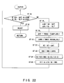
- the estimated correction values ( ⁇ VC and ⁇ VBG) as well as new image forming conditions (VG and VD) can be obtained according to the following algorithm using the above parameters, as shown by the flow chart of Fig. 22.
- the toner attaching amount measurement sequence can be executed by controller 45.
- ⁇ VC and ⁇ VBG can be obtained by measuring potential differences VC, VC*, VBG, and VBG* of surface potentials VL and VO with respect to developing bias potential VD, respectively, at two grid biases -VG and -VG ⁇ .
- the values of QH and QL for calculating ⁇ QH and ⁇ QL can be measured according to the relation shown in Fig. 9 or 11 which will be mentioned later. Based on ⁇ VC, ⁇ VBG, ⁇ QH, and ⁇ QL thus obtained, the contents of TABLE C and TABLE BG can be determined with actual measurement. These tables may be stored in memory 387 shown in Fig. 2A.
- Fig. 8 shows image density ID of a painted portion, or toner attaching amount Q, as a function of exposure amount P of a laser beam.
- This embodiment uses a region where image density ID begins to be saturated with respect to exposure amount P.
- a low-density portion is mainly changed (see Fig. 9). Therefore, correction can be performed by changing the exposure amount with reference to a variation of the low-density portion.
- Fig. 10 shows the relationship between toner density T/D and toner attaching amount Q.
- Toner attaching amount Q monotonously increases as a function of toner density T/D.
- a toner density lower limit value is determined by experiences based on attachment of the carrier onto photosensitive drum 1
- another toner density upper limit value is determined by experiences based on problems such as an increase in non-charged toner. The toner density is changed within a range defined between these values.
- Fig. 11 shows a change in toner attaching amount Q as a function of gradation data when the toner density is increased.
- Fig. 12 shows image data, laser exposure time (pulse width) PD, toner attaching amount Q, and printer output image density ID.
- laser exposure time PD, toner attaching amount Q, and printer output image density ID for given gradation data have a correspondence therebetween.
- toner attaching amount Q varies (alternate long and short dashed curve g) due to a deterioration over time or a change in environment, the relationship between image data and toner attaching amount Q can be made constant by changing the contents of a conversion table between gradation data and laser exposure time PD (alternate long and two short dashed curve h).
- the above conversion table can be stored in memory 387 shown in Fig. 2A.
- This embodiment has a larger number of levels (e.g. 4096 levels) of laser exposure time PD than that of gradation data (256 levels), and may be provided with a selection circuit by which various laser exposure times PD each corresponding to gradation data can be optionally selected.
- Toner sensor 8 will be described in detail below.
- Fig. 13 shows an arrangement of toner sensor 8.
- light from light source 51 is radiated on the surface of photosensitive drum 1.
- Light reflected by the surface of photosensitive drum 1, or by toner DM developed and attached on drum 1 is converted into a current according to the amount of reflected light by photoelectric conversion section 52, and the current is then current-to-voltage converted into signal E52.
- Signal E52 is supplied to A/D converter 46 through transmission circuit 53, and is converted into digital signal D46.
- Digital signal D46 represents the amount (Q) of toner DM attached on drum 1, and is fetched by controller 45.
- Light source 51 is driven by output current I54 from light source driver 54.
- Light source driver 54 is ON/OFF-controlled by control signal E451 from controller 45, and adjusts the amount of drive current I54 input to light source 51 according to signal E451.
- Fig. 14 shows the spectral reflectances of output images. More specifically, Fig. 14 shows the spectral reflectances of images obtained by solely outputting yellow Y, magenta M, cyan C, and black BK toners using a color printer.
- Figs. 15 and 15A show the mirror surface reflectances of photosensitive drum 1 at different incident angles.
- a mirror surface reflectance at a relatively shallow (or small) angle ( ⁇ ) with respect to the normal to the reflection surface of drum 1 is represented by curve o
- a mirror surface reflectance at a deep (or large) angle ( ⁇ ) is represented by broken curve p.
- Fig. 15 teaches that the wavelength dependency of reflection is reduced as the angle ( ⁇ ) becomes deeper.
- Fig. 16A explains how reflectance R can be obtained.
- the reference symbol A denotes an input light beam with incidence angle ⁇ 1; R, an reflected light beam with reflection angle ⁇ 1; and D, a transit light beam running from refractive index n1 area to refractive index n2 area, with angle ⁇ 2.
- rT amplitude reflection factor r of the parallel component with respect to the incidence angle
- RT reflectance R of the parallel component with respect to the incidence angle
- RS perpendicular component with respect to reflectance R
- ⁇ B is 57.777 degrees.
- a shallow incident angle is set for color toners (Y, M, and C), and the wavelength of light emitted from light source 51 is set to fall within a wavelength region of 800 nm or higher, thus widening the dynamic range.
- a black toner light is caused to become incident at a relatively deep angle, and the wavelength range is not limited to a range between 300 nm and 1,000 nm.
- the photosensitivity of the photosensitive drum has a high level in a wavelength range between 500 nm and 800 nm, the wavelength in this range is not used so as to avoid stray light to an image region due to mirror surface reflection, scattering of a toner image as an object to be measured, and the like.
- a wavelength other than a wavelength 1/10 the highest sensitivity level i.e., a wavelength of 860 nm or higher, and preferably, a wavelength falling within a range of 860 nm and 1,000 nm was selected.
- photoelectric conversion section 52 a photodiode having a sensitivity (a conversion current amount with respect to a received light amount) shown in Fig. 18 was used.
- Fig. 19 shows a state of a shielding member arranged between toner sensor 8 and photosensitive drum 1. More specifically, toner sensor 8 is arranged, so that its measurement surface opposes the surface of photosensitive drum 1. Plate-like shielding member 61 is arranged to be able to be opened/closed in the vicinity of the measurement surface side of toner sensor 8. One end of shielding member 61 is coupled to flapper 63 of solenoid 62 via a pin. Shielding member 61 is moved to the right and left, i.e., in a direction of a double-headed arrow X in Fig. 19 according to an opening/closing operation of flapper 63 upon an ON/OFF operation of solenoid 62.
- Shielding member 61 is closed in a non-measurement mode of toner sensor 8, thereby shielding the measurement surface from external environment. Shielding member 61 is opened in only a measurement mode, thus eliminating the measurement surface from being contaminated with a scattered toner. As a result, a period allowing high-accuracy measurement can be prolonged.
- the amount of a toner attached on the photosensitive drum upon development is measured.
- the measured toner attaching amount is compared with a predetermined reference value.
- At least one of the charging amount for the photosensitive drum, the developing bias voltage, the exposure amount, the toner density, and the like is changed on the basis of the comparison result.
- Fig. 20 shows another arrangement of toner sensor 8.
- the same reference numerals in Fig. 20 denote the same parts as in Fig. 13, and a detailed description thereof will be omitted. Thus, only different portions will be described below.
- light from light source 51 is radiated on the surface of photosensitive drum 1.
- Light reflected by the surface of photosensitive drum 1, or by a toner developed and attached on drum 1 is converted into currents according to the amount of reflected lights L1 and L2 by first and second photoelectric conversion sections 52 and 55, and the currents are respectively current-to-voltage converted into signals E52 and E55.
- Signals E52 and E55 are supplied to A/D converter 46 through transmission circuits 53 and 56, and are converted into digital signal D46.
- Digital signal D46 is then fetched by controller 45.
- First photoelectric conversion section 52 is arranged at a position where it can receive reflected light including principal ray L1 obtained upon reflection of the principal ray emitted from light source 51 by the surface of photosensitive drum 1
- second photoelectric conversion section 55 is arranged at a position where it can receive reflected light L2 including no principal ray obtained upon reflection of the principal ray emitted from light source 51 by the surface of photosensitive drum 1.
- first photoelectric conversion section 52 receives mirror surface reflected light L1 by the surface of photosensitive drum 1
- second photoelectric conversion section 55 receives divergent reflected light L2 by the surface of photosensitive drum 1.
- Fig. 21 shows first and second photoelectric conversion sections 52 and 55, and the reflected light distribution of photosensitive drum 1.
- Principal ray l from light source 51, and principal ray L1 of light reflected by photosensitive drum 1 are indicated by an alternate long and short dashed curve.
- Divergent reflected light L2 is indicated by a broken curve.
- Solid curve m represents the reflected light distribution on photosensitive drum 1 on which no toner is attached.
- the light amount (L1) based on mirror surface reflection of the surface of photosensitive drum 1 and the conductive support member for supporting a photosensitive layer is large.
- divergent light scattered by the surface of the photosensitive drum, the photosensitive layer, and the conductive support member is detected.
- divergent reflected light (L2) has a smaller light amount than that of mirror surface reflected light (L1).
- first photoelectric conversion section 52 measures the amount of decrease in mirror surface reflected light (L1)
- second photoelectric conversion section 55 measures the amount of increase in divergent reflected light (L2).
- the toner attaching amount In measurement of the toner attaching amount by mirror surface reflected light, when the toner attaching amount exceeds a given value, a change in light amount of mirror surface reflected light becomes very small. When the toner attaching amount is decreased below a given value, the light amount of divergent reflected light becomes smaller than that on photosensitive drum 1 on which no toner is attached although it depends on a particular toner and photosensitive body used.
- an image forming apparatus which can correct an image density drift caused by a change in environment or a deterioration over time independently of the maintenance, and at a shorter cycle than the maintenance cycle, can stabilize a high image density, and can reduce maintenance cost, can be provided.
Description
- The present invention relates to an electrophotographic color image forming apparatus such as a color laser printer, a color digital copying machine, and the like.
- For example, many users experience that copies obtained by copying the same original using the same copying machine have different densities. In an electrophotograph, an image density drift occurs under the influence of a change or deterioration of image forming conditions due to different environmental factors and an elapse of time. It is important for a multi-level printer or a digital copying machine as well as an analog copying machine to suppress and stabilize the image density drift. In particular, in a color image, since the image density drift influences not only density reproducibility but also color reproducibility, a stable image density is an indispensable requirement. Therefore, in a conventional apparatus, a given allowable margin is provided to image forming materials and an image forming process itself, and image stabilization is attained by maintenance within this allowable margin.
- However, the allowable margin to be provided to the image forming materials and image forming process itself is limited, and the maintenance requires much labor and cost. Furthermore, the image density drift cycle is shorter than a maintenance cycle, and a stable image density cannot always be obtained by only the maintenance.
- GB-A-2 212 419 discloses a color image forming apparatus wherein, for each of the colors, toner test patterns are generated on an image carrier and the low density portion and medium density portion of the pattern is compared to respective reference values. The high density portion is controlled by means of a sensor provided in the developing unit.
- It is an object of the present invention to provide acolorimage forming apparatus, which can correct an image density drift due to a change in environment or a deterioration over time independently of the maintenance and at a shorter cycle than the maintenance cycle, can stabilize a high image density, and can reduce maintenance cost.
- The above objects are achieved by an image forming apparatus as defined in
claim 1. - The amount of the developing agent attached on the image carrier upon development is measured. The measured attaching amount of the developing agent is compared with a predetermined reference value. At least one of the charging amount for the image carrier, the developing bias voltage, the exposure amount, the density of the developing agent, and the like is changed on the basis of the comparison result. Thus, an image density drift due to a change in environment or a deterioration over time can be corrected independently of the maintenance, and at a shorter cycle than the maintenance cycle. As a result, a high image density can be stabilized, and cost (labor cost, equipment, and the like) required for the maintenance can be reduced.
- This invention can be more fully understood from the following detailed description when taken in conjunction with the accompanying drawings, in which:
- Fig. 1 is a schematic sectional view of a color laser printer;
- Fig. 2 is a block diagram showing charging, exposure, and developing means of a color laser printer according to an embodiment of the present invention, and their control means for one color;
- Fig. 2A is a block diagram showing the internal configuration of the laser driver and the pattern generator shown in Fig. 2;
- Fig. 3 is a graph showing the toner attaching amount as a function of gradation data;
- Fig. 4 is a graph showing the potentials of non-exposed and exposed portions of a photosensitive drum, and the developing bias voltage as a function of the grid bias voltage of a charger;
- Fig. 5 is a graph showing the image density of a painted portion as a function of the contrast potential;
- Fig. 6 is a graph showing the relationship among the potential of a non-exposed portion of the photosensitive drum, the potential by a low-density pattern, and the developing bias voltage;
- Fig. 7 is a graph showing the toner attaching amount as a function of gradation data obtained when the background potential is changed;
- Fig. 8 is a graph showing the image density of a painted portion as a function of the exposure amount;
- Fig. 9 is a graph showing the toner attaching amount as a function of gradation data obtained when the exposure amount is changed;
- Fig. 10 is a graph showing the relationship between the toner density and the toner attaching amount;
- Fig. 11 is a graph showing a change in toner attaching amount as a function of gradation data when the toner density is increased;
- Fig. 12 is a graph showing the relationship among image data, the laser exposure time, the toner attaching amount, and the printer output image density;
- Fig. 13 is a block diagram showing an arrangement of a toner sensor;
- Fig. 14 is a graph showing the spectral reflectance of a printer output image;
- Figs. 15 and 15A show the mirror surface reflectance of the photosensitive drum at different light incident angles;
- Fig. 16 is a graph showing the reflection characteristics of a photosensitive drum surface as a function of the light incident angle;
- Fig. 16A explains how the reflectance can be obtained;
- Fig. 17 is a graph showing the photosensitivity characteristics of the photosensitive drum;
- Fig. 18 is a graph showing the photosensitivity characteristics of a photoelectric conversion unit;
- Fig. 19 is a view showing a state of a shielding member arranged between the toner sensor and the photosensitive drum;
- Fig. 20 is a block diagram showing another arrangement of the toner sensor;
- Fig. 21 is a view showing first and second photoelectric conversion units, and the reflected light distribution of a photosensitive drum shown in Fig. 20; and
- Fig. 22 is a flow chart explaining the algorithm for obtaining image forming conditions.
- An embodiment of the present invention will be described hereinafter with reference to the accompanying drawings.
- Fig. 1 shows an arrangement of a color laser printer as an embodiment of an image forming apparatus according to the present invention. In Fig. 1,
reference numeral 1 denotes a photosensitive drum as an image carrier, which is rotated counterclockwise with respect to the drawing surface.Charger 2 as a charging means, first, second, third, and fourth developingunits toner sensor 8,transfer drum 9 as a transfer medium support member, pre-cleaningdischarger 10,cleaner 11, and discharginglamp 12 are sequentially arranged aroundphotosensitive drum 1. -
Photosensitive drum 1 is rotated in the direction of an arrow in Fig. 1, and its surface is uniformly charged bycharger 2. The surface ofphotosensitive drum 1 is exposed bylaser beam 14 emerging fromoptical system 13 as an exposure means through a portion betweencharger 2 and first developingunit 4, thereby forming an electrostatic latent image according to image data. - First to fourth developing
units 4 to 7 visualize electrostatic latent images corresponding to respective colors onphotosensitive drum 1 to color toner images, using prescribed developing materials. For example, first developingunit 4 performs magenta development, second developing unit 5 performs cyan development, third developingunit 6 performs yellow development, and fourth developing unit 7 performs black development. - Meanwhile, a transfer sheet as a transfer medium is fed from
paper feed cassette 15 bypaper feed roller 16, and is temporarily registered by registration rollers 17. The sheet is then fed by registration rollers 17, so that it is attracted at a predetermined position oftransfer drum 9. The sheet is electrostatically attached ontransfer drum 9 byattraction roller 18 andattraction charger 19. The transfer sheet is conveyed upon clockwise rotation oftransfer drum 9 while being attracted ontransfer drum 9. - The developed toner image on
photosensitive drum 1 is transferred onto the transfer sheet bytransfer charger 20 at a position wherephotosensitive drum 1 opposestransfer drum 9. In a multi-color printing operation, a process that defines one cycle by one revolution oftransfer drum 9 is performed while switching the developing unit. As a result, a plurality of color toner images are multiple-transferred onto the transfer sheet. - The transfer sheet on which the toner images are transferred is further conveyed upon rotation of
transfer drum 9, and is discharged by pre-peelinginner discharger 21, pre-peelingouter discharger 22, andpeeling discharger 23. Thereafter, the sheet is peeled fromtransfer drum 9 bypeeling pawl 24, and is then conveyed to fixingunit 27 byconveyor belts fixing unit 27, are melted, and are fixed on the transfer sheet immediately after the sheet is delivered fromfixing unit 27. The transfer sheet after the fixing operation is delivered ontotray 28. - Fig. 2 is a block diagram showing charging, exposure, and developing means of a color laser printer according to an embodiment of the present invention, and their control means. In Fig. 2,
photosensitive drum 1 is rotated counterclockwise (in the direction of an arrow in Fig. 2) with respect to the drawing surface.Charger 2 mainly comprises chargingwire 31, conductive case 32, andgrid electrode 33. Chargingwire 31 is connected to corona high-voltage power supply 34, and performs corona discharging to charge the surface ofphotosensitive drum 1.Grid electrode 33 is connected to grid bias high-voltage power supply 35, and controls the charging amount on the surface ofphotosensitive drum 1 according to a grid bias voltage. - The surface, uniformly charged by
charger 2, ofphotosensitive drum 1 is exposed by modulatedlaser beam 14 fromoptical system 13, thereby forming an electrostatic latent image thereon.Gradation data buffer 36 stores gradation data (image data) from an external apparatus (not shown) orcontroller 45, corrects printer gradation characteristics of the stored data, and converts it into laser exposure time (pulse width) data. -
Laser driver 37 modulates a laser drive current (light emission time) according to laser exposure time data D36 fromgradation data buffer 36 in synchronism with a scan position oflaser beam 14. The modulated laser drive current drives a semiconductor laser oscillator (not shown) inoptical system 13. Thus, the semiconductor laser oscillator performs a light-emission operation according to the exposure time data. - Furthermore,
laser driver 37 compares an output from a monitor light-receiving element (not shown) inoptical system 13 with a set value so as to make control for maintaining the output light amount of the semiconductor laser oscillator to be the set value using drive current I37. (This control is performed byAPC circuit 3704 in Fig. 2A.) - On the other hand,
pattern generator 38 generates gradation data D38 for a test pattern of the printer, and for a pattern used in toner attaching amount measurement, and sends it tolaser driver 37. - Fig. 2A is a block diagram exemplifying the internal configuration of
laser driver 37 andpattern generator 38. -
Controller 45 exchanges command/status between microprocessor (MPU) 380 inpattern generator 38, andsupplies selector 381 with, for example, image data of 8-bit/pixel and 10MHz video clock VCLK in response to the contents of the command/status. - Also supplied to
selector 381 are 8-bit/pixel image data (256-color or 256-gray scale) for producing a predetermined test pattern and 10 MHz video clock VCLK, obtained fromtest pattern generator 382. - When a normal print is performed,
selector 381 selects the image data and video clock fromcontroller 45 in response to selection instruction S1 fromMPU 380. When toner attaching amount Q is to be detected,selector 381 selects the image data (D38) and video clock fromtest pattern generator 382. - The content of the test pattern generated by
test pattern generator 382 can be optionally changed to other desired patterns in accordance with a prescribed software executed byMPU 380 usingmemory 387. - The image data and video clock VCLK selected by
selector 381 are input topixel counter 383. Counter 383 counts clock VCLK during a period in which the image data exceeds a predetermined level. Count data D383 corresponding to this period is fed back toMPU 380 fromcounter 381. In response to fed-back count data D383,MPU 380 checks the contents of the image data output fromselector 381. - 10 MHz video clock VCLK selected by
selector 381 is input toselectors 371 and 372 inlaser driver 37. The image data selected byselector 381 is input to selector 377 inlaser driver 37. - Each of
selectors 371 and 372 selects either of 10 MHz video clock VCLK and 21 MHz sync clock CLK370 sent fromgate 370, in response to the signal level of HSYNC output S133 from horizontal sync (HSYNC)detector 133. - Sync clock CLK370 is obtained by gating the 21 MHz output of sync cock generator 3701 with a signal indicating a prescribed print area. The 21 MHz output of generator 3701 in produced from 21 MHz/42 MHz
primary crystal oscillator 3700 in synchronization with HSYNC output S133. - One of clocks VCLK and CLK370 selected by
selector 371 or 372 is counted bycounter - The count result of
counter line buffer 375 or 376 whenselector 371 or 372 changes its selection state. The data written in buffer 375 is sent to one output circuit of selector 377, and the data written inbuffer 376 is sent to the other output circuit of selector 377. - The two outputs of selector 377 are input to
selector 378. Selector 377 sends the image data fromselector 381 to one of its two output circuits, in response to the signal level of HSYNC output S133 fromHSYNC detector 133. - In response to the signal level of HSYNC output S133,
selector 378 selects one of the two outputs of selector 377, on which the outputs ofbuffers 375 and 376 are imposed. The selected test pattern data of, for example 8-bit/21 MHz, is input to pulse width modulation (PWM)circuit 3702. - In response to HSYNC output S133 from
HSYNC detector 133,PWM circuit 3702 supplieslaser driver 3703 with PWM signal S3702 corresponding to input test pattern data (image data). - In response to PWM signal S3702,
laser driver 3703 controls drive current 137 forlaser diode 130 on the basis of control output S3704 from automatic power control (APC)circuit 3704. Monitor output S130 indicating the driving state oflaser diode 130 is fed back tocontrol circuit 3704. - The laser beam emitted from
laser diode 130 is reflected by a rotating mirror driven bymirror motor 131, so that the reflected beam scans overphotosensitive drum 1 shown in Fig. 2. The reflection beam of the scanning beam is detected byHSYNC detector 133, anddetector 133 generates HSYNC output S133 in synchronization with the scanning (horizontal scanning). -
Mirror motor 131 is driven bymirror motor driver 132. A mirror motor on instruction and mirror motor ready instruction are exchanged betweenMPU 380 anddriver 132 in order to controlmirror motor 131. - HSYNC output S133 is input to APC counter 384 controlled by
MPU 380. Counter S133 also serves as a top/bottom margin counter of a print area (or imaging region IR1). HSYNC output S133 is also input to right/left margin counter 385 for the print area and to sampletimer 386 for controlling the sampling of PWM signal S3702. - Further input to counter 385 and
timer 386 is a margin clock which is obtained by frequency-dividing the 21 MHz output from sync clock generator 3701, byfrequency divider 379. -
MPU 380 controls the operations ofAPC circuit 3704 andlaser driver 3703 while performing signal exchanges withcounters timer 386. These controls further includes laser power monitors (analog/digital), data exchanges, a clock supply, data latching, a print area designation, a sample designation, a laser drive enable. -
Photosensitive drum 1 on which an electrostatic latent image is formed is developed by developingunit 4. Developingunit 4 employs, e.g., a two-component developing system, and stores developing agent DM consisting of a toner and a carrier. The weight ratio (T/D) of the toner to the developing agent (to be referred to as a toner density hereinafter) is measured bytoner density sensor 39.Toner replenishment motor 41 for drivingtoner replenishment roller 40 is controlled according to output A39 fromtoner density sensor 39, so that the toner intoner hopper 42 is replenished into developingunit 4. - Developing
roller 43 of developingunit 4 is formed of a conductive member, and is connected to developing bias high-voltage power supply 44.Roller 43 is rotated while being applied with a developing bias voltage, and causes a toner to become attached to an image according to the electrostatic latent image onphotosensitive drum 1. A toner image developed in this manner in imaging region IR is transferred onto a transfer sheet, which is supported and conveyed bytransfer drum 9. Region IR is formed of actual imaging region IR1 and non-imaging region IR2. -
Controller 45, comprising a microcomputer, switches data to be input tolaser driver 37 from laser exposure time data D36 fromgradation data buffer 36 to gradation data D38 frompattern generator 38 in synchronism with a timing at which the exposure position onphotosensitive drum 1 reaches the position of non-imaging region IR2, thereby exposing a gradation pattern (e.g., a gray scale) for measuring a toner attaching amount on non-image region IR2 onphotosensitive drum 1. - The above-mentioned synchronizing switch operation by
controller 45 can be achieved as follows. - A sensor (not shown) for sensing the leading edge position of a print paper is located at the
cassette 15 side nearroller 18 shown in Fig. 18. This sensor may be formed of a photo-interrupter comprising a pair of an LED and the photo diode. The optical path between the LED and the photo diode is interrupted by the leading edge of the paper. - When the sensor senses the leading edge of the paper fed from the
cassette 15 side, a timer (not shown) starts. According to the time passage measured by this timer,controller 45 is informed of the timing that the non-image area on a predetermined position of the paper being fed with a constant speed reaches the exposure position ofdrum 1. -
Toner sensor 8 measures toner attaching amount Q in synchronism with a timing at which the position onphotosensitive drum 1, where the gradation pattern is exposed, is developed, and reaches the position oftoner sensor 8. Output A8 fromtoner sensor 8, and output A39 fromtoner density sensor 39 are digitized by A/D converter 46, and digital output D46 is input tocontroller 45. -
Controller 45 compares data corresponding to output (measurement value) A8 fromtoner sensor 8 with a predetermined reference value, and executes processing for changing at least one of the grid bias voltage (VG) ofcharger 2, the developing bias voltage (VD) of developingunit 4, the exposure amount (P) ofoptical system 13, the toner density (T/D) of the developing agent, the light-emission time (P/D) of area gradation, and the like as image forming conditions according to the comparison result. - The control of voltage VG is effected on
power supply 35; voltage VD, onpower supply 44; exposure amount P and light-emission time PD, onoptical system 13; and toner density T/D, onmotor 41. -
Controller 45 performs switching control between gradation data from an external apparatus or controller (neither are shown), and gradation data for a test pattern of the printer, and a pattern used in toner attaching amount measurement, fetching control of outputs fromsensors - Fig. 3 shows toner attaching amount Q as a function of gradation data (D46). A curve representing the toner attaching amount as a function of gradation data can be obtained by an actual measurement. This curve is affected by a deviation caused by variations in image forming conditions due to a deterioration over time and a change in environment. Therefore, a small variation of the curve representing the toner attaching amount as a function of gradation data due to a deterioration over time and a change in environment is a necessary condition for stabilizing the image density.
- Fig. 4 shows surface potential (to be referred to as non-exposed portion potential hereinafter) V0 of
photosensitive drum 1 uniformly charged bycharger 2, attenuated surface potential (to be referred to as exposed portion potential hereinafter) VL ofphotosensitive drum 1, after the entire surface ofdrum 1 is exposed by a constant light amount byoptical system 13, and developing bias voltage VD (an alternate long and short dashed line) with respect to absolute value VG of a bias voltage (to be simply referred to as a grid bias voltage hereinafter) forgrid electrode 33 ofcharger 2. - Since reversal development is performed in this embodiment, a potential or voltage has negative polarity. When grid bias voltage VG is increased, nonexposed portion potential V0 and exposed portion potential VL are respectively decreased. Non-exposed portion potential V0 and exposed portion potential VL for grid bias voltage VG can be linearly approximated as follows:


- The developing density changes according to the relationship among developing bias voltage VD, exposed portion potential VL, and non-exposed portion potential V0. Assume that contrast potential VC and background potential VBG are defined as follows:


- Contrast potential VC depends on the density QH as defined below (especially the maximum density) of a painted portion (see Fig. 5). Background potential VBG is mainly associated with the density of a low-density portion in a multi-level system using pulse width modulation (see Fig. 6).
- Fig. 7 shows toner attaching amount Q as a function of gradation data when background potential VBG is increased. A low-density region is shifted in a direction of an arrow C in Fig. 7. Therefore, the developing density can be changed by contrast potential VC and background potential VBG.
- The following equations are obtained from equations (1) to (4):


- From equations (5) and (6), when the relationship (K1, K2) of exposed portion potential VL and non-exposed portion potential V0 with respect to grid bias voltage VG is known, grid bias voltage VG and developing bias voltage VD can be uniquely determined by determining contrast potential VC and background potential VBG.
- The surface potential of
photosensitive drum 1 is measured in advance to obtain the relationship (K1, K2) of exposed portion potential VL and non-exposed portion potential V0 with respect to grid bias voltage VG. Thereafter, contrast potential VC and background potential VBG are set. From equations (5) and (6), grid bias voltage VG and developing bias voltage VD are uniquely determined. Under this condition, a plurality of density ?atterns are formed, and toner attaching amounts Q of these patterns after development are measured. The measured amounts are then compared with a predetermined reference value. Based on deviations ΔQ between the measured amounts and the reference value, correction values ΔVC and ΔVBG of contrast potential VC and background potential VBG for a proper developing density are estimated. Grid bias voltage VG and developing bias voltage VD are set again according to the estimation results, and the toner attaching amounts of the density patterns are measured. These operations are repeated until these voltages fall within an allowable range. - Now, the following parameters are defined:
- QH: measured value of toner attaching amount for high density portion of test pattern
- QL: measured value of toner attaching amount for low density portion of test pattern
- QHT: reference value of toner attaching amount for high density portion of test pattern
- QLT: reference value of toner attaching amount for low density portion of test pattern
- ΔQHP: specific control value of toner attaching amount for high density portion of test pattern
- ΔQLP: specific control value of toner attaching amount for low density portion of test pattern
- ΔVC: contrast potential change value (correction value)
- ΔVBG: background potential change value (correction value)
- VG: grid bias potential after change
- VD: developing bias potential after change
- The estimated correction values (ΔVC and ΔVBG) as well as new image forming conditions (VG and VD) can be obtained according to the following algorithm using the above parameters, as shown by the flow chart of Fig. 22.

- Using the values of VG and VBG obtained according to the above algorithm, the toner attaching amount measurement sequence can be executed by
controller 45. - Incidentally, as shown in Fig. 4, ΔVC and ΔVBG can be obtained by measuring potential differences VC, VC*, VBG, and VBG* of surface potentials VL and VO with respect to developing bias potential VD, respectively, at two grid biases -VG and -VG∗.
- The values of QH and QL for calculating ΔQH and ΔQL can be measured according to the relation shown in Fig. 9 or 11 which will be mentioned later. Based on ΔVC, ΔVBG, ΔQH, and ΔQL thus obtained, the contents of TABLE C and TABLE BG can be determined with actual measurement. These tables may be stored in
memory 387 shown in Fig. 2A. - Fig. 8 shows image density ID of a painted portion, or toner attaching amount Q, as a function of exposure amount P of a laser beam. This embodiment uses a region where image density ID begins to be saturated with respect to exposure amount P. When the light amount is changed, a low-density portion is mainly changed (see Fig. 9). Therefore, correction can be performed by changing the exposure amount with reference to a variation of the low-density portion.
- Fig. 10 shows the relationship between toner density T/D and toner attaching amount Q. Toner attaching amount Q monotonously increases as a function of toner density T/D. A toner density lower limit value is determined by experiences based on attachment of the carrier onto
photosensitive drum 1, and another toner density upper limit value is determined by experiences based on problems such as an increase in non-charged toner. The toner density is changed within a range defined between these values. - Fig. 11 shows a change in toner attaching amount Q as a function of gradation data when the toner density is increased.
- Fig. 12 shows image data, laser exposure time (pulse width) PD, toner attaching amount Q, and printer output image density ID. When a color laser printer to which the present invention is applied is part of a digital copying machine, laser exposure time PD, toner attaching amount Q, and printer output image density ID for given gradation data have a correspondence therebetween. When toner attaching amount Q varies (alternate long and short dashed curve g) due to a deterioration over time or a change in environment, the relationship between image data and toner attaching amount Q can be made constant by changing the contents of a conversion table between gradation data and laser exposure time PD (alternate long and two short dashed curve h). The above conversion table can be stored in
memory 387 shown in Fig. 2A. This embodiment has a larger number of levels (e.g. 4096 levels) of laser exposure time PD than that of gradation data (256 levels), and may be provided with a selection circuit by which various laser exposure times PD each corresponding to gradation data can be optionally selected. - Incidentally, the mutual relation among Q, ID, and VC can be read from a combination of the graphs of Figs. 5 and 12.
-
Toner sensor 8 will be described in detail below. - Fig. 13 shows an arrangement of
toner sensor 8. In Fig. 13, light fromlight source 51 is radiated on the surface ofphotosensitive drum 1. Light reflected by the surface ofphotosensitive drum 1, or by toner DM developed and attached ondrum 1, is converted into a current according to the amount of reflected light byphotoelectric conversion section 52, and the current is then current-to-voltage converted into signal E52. Signal E52 is supplied to A/D converter 46 throughtransmission circuit 53, and is converted into digital signal D46. Digital signal D46 represents the amount (Q) of toner DM attached ondrum 1, and is fetched bycontroller 45. -
Light source 51 is driven by output current I54 fromlight source driver 54.Light source driver 54 is ON/OFF-controlled by control signal E451 fromcontroller 45, and adjusts the amount of drive current I54 input tolight source 51 according to signal E451. - Fig. 14 shows the spectral reflectances of output images. More specifically, Fig. 14 shows the spectral reflectances of images obtained by solely outputting yellow Y, magenta M, cyan C, and black BK toners using a color printer.
- Figs. 15 and 15A show the mirror surface reflectances of
photosensitive drum 1 at different incident angles. In Fig. 15, a mirror surface reflectance at a relatively shallow (or small) angle (θ) with respect to the normal to the reflection surface ofdrum 1 is represented by curve o, and a mirror surface reflectance at a deep (or large) angle (θ) is represented by broken curve p. Fig. 15 teaches that the wavelength dependency of reflection is reduced as the angle (θ) becomes deeper. (Fig. 15A exemplifies the case where reflectance R = 53% is obtained at wavelength λ = 510 nm, and R = 11% is obtained at λ = 800 nm.) - This can also understood from the fact that reflection of the surface of a polycarbonate (refractive index = 1.586) has characteristics with respect to the incident angle, as shown in Fig. 16. In Fig. 16, curve RT represents a reflectance in a direction parallel to the incident angle, and curve RS represents a reflectance in a direction perpendicular to the incident angle. Therefore, when the incident angle is shallow, the amount of light, which is transmitted through a photosensitive layer of the photosensitive drum, is reflected by a conductive support member, having a metallic gross, for supporting the photosensitive layer, and is again transmitted through the photosensitive layer, is larger than that of light reflected by the surface of the photosensitive drum.
- Fig. 16A explains how reflectance R can be obtained. In the figure, the reference symbol A denotes an input light beam with incidence angle θ₁; R, an reflected light beam with reflection angle θ₁; and D, a transit light beam running from refractive index n1 area to refractive index n2 area, with angle θ₂.
- Assume that amplitude reflection factor r of the parallel component with respect to the incidence angle is denoted by rT; that reflectance R of the parallel component with respect to the incidence angle is denoted by RT; and that the perpendicular component with respect to reflectance R is denoted by RS.
- Since the relation "n1·sinθ₁ = n2·sinθ₂" is obtained from the Snell laws of refraction, the following equations are derived from the Fresnel's formulas:

- In Fig. 16, parallel component RT becomes zero at Brewster's angle (polarizing angle) θB of incidence angle θ(= θ₁). (In the embodiment wherein the main component of a paper is polycarbonate, θB is 57.777 degrees.)
- When a polarizing filter (not shown) is arranged in front of a photodetector (not shown) in toner attaching
amount sensor 8 so that perpendicular component RS input to the photodetector is cut out, direct reflection light tosensor 8 can be eliminated provided that parallel component RT is cancelled out with Brewster's angle θB. Further, complete elimination of the direct reflection light can be avoided, if the angle of the polarizing filter is adjusted so as to guide a desired amount of the direct reflection light tosensor 8. - In in the case of
photosensitive drum 1 of this embodiment, a shallow incident angle is set for color toners (Y, M, and C), and the wavelength of light emitted fromlight source 51 is set to fall within a wavelength region of 800 nm or higher, thus widening the dynamic range. As for a black toner, light is caused to become incident at a relatively deep angle, and the wavelength range is not limited to a range between 300 nm and 1,000 nm. - However, as shown in Fig. 17, since the photosensitivity of the photosensitive drum has a high level in a wavelength range between 500 nm and 800 nm, the wavelength in this range is not used so as to avoid stray light to an image region due to mirror surface reflection, scattering of a toner image as an object to be measured, and the like. In this embodiment, a wavelength other than a
wavelength 1/10 the highest sensitivity level, i.e., a wavelength of 860 nm or higher, and preferably, a wavelength falling within a range of 860 nm and 1,000 nm was selected. In this case, asphotoelectric conversion section 52, a photodiode having a sensitivity (a conversion current amount with respect to a received light amount) shown in Fig. 18 was used. - Fig. 19 shows a state of a shielding member arranged between
toner sensor 8 andphotosensitive drum 1. More specifically,toner sensor 8 is arranged, so that its measurement surface opposes the surface ofphotosensitive drum 1. Plate-like shielding member 61 is arranged to be able to be opened/closed in the vicinity of the measurement surface side oftoner sensor 8. One end of shieldingmember 61 is coupled toflapper 63 ofsolenoid 62 via a pin. Shieldingmember 61 is moved to the right and left, i.e., in a direction of a double-headed arrow X in Fig. 19 according to an opening/closing operation offlapper 63 upon an ON/OFF operation ofsolenoid 62. - Shielding
member 61 is closed in a non-measurement mode oftoner sensor 8, thereby shielding the measurement surface from external environment. Shieldingmember 61 is opened in only a measurement mode, thus eliminating the measurement surface from being contaminated with a scattered toner. As a result, a period allowing high-accuracy measurement can be prolonged. - In this manner, according to the above embodiment, the amount of a toner attached on the photosensitive drum upon development is measured. The measured toner attaching amount is compared with a predetermined reference value. At least one of the charging amount for the photosensitive drum, the developing bias voltage, the exposure amount, the toner density, and the like is changed on the basis of the comparison result. Thus, an image density drift due to a change in environment or a deterioration over time can be corrected independently of the maintenance, and at a shorter cycle than the maintenance cycle. As a result, a high image density can be stabilized, and cost (labor cost, equipment, and the like) required for the maintenance can be reduced.
- Fig. 20 shows another arrangement of
toner sensor 8. The same reference numerals in Fig. 20 denote the same parts as in Fig. 13, and a detailed description thereof will be omitted. Thus, only different portions will be described below. In Fig. 20, light fromlight source 51 is radiated on the surface ofphotosensitive drum 1. Light reflected by the surface ofphotosensitive drum 1, or by a toner developed and attached ondrum 1, is converted into currents according to the amount of reflected lights L1 and L2 by first and secondphotoelectric conversion sections D converter 46 throughtransmission circuits controller 45. - First
photoelectric conversion section 52 is arranged at a position where it can receive reflected light including principal ray L1 obtained upon reflection of the principal ray emitted fromlight source 51 by the surface ofphotosensitive drum 1, and secondphotoelectric conversion section 55 is arranged at a position where it can receive reflected light L2 including no principal ray obtained upon reflection of the principal ray emitted fromlight source 51 by the surface ofphotosensitive drum 1. Thus, firstphotoelectric conversion section 52 receives mirror surface reflected light L1 by the surface ofphotosensitive drum 1, and secondphotoelectric conversion section 55 receives divergent reflected light L2 by the surface ofphotosensitive drum 1. - Fig. 21 shows first and second
photoelectric conversion sections photosensitive drum 1. Principal ray ℓ fromlight source 51, and principal ray L1 of light reflected byphotosensitive drum 1 are indicated by an alternate long and short dashed curve. Divergent reflected light L2 is indicated by a broken curve. - Solid curve m represents the reflected light distribution on
photosensitive drum 1 on which no toner is attached. At angle θ of principal ray ℓ of reflected light, the light amount (L1) based on mirror surface reflection of the surface ofphotosensitive drum 1 and the conductive support member for supporting a photosensitive layer is large. At an angle other than angle θ, divergent light scattered by the surface of the photosensitive drum, the photosensitive layer, and the conductive support member is detected. Thus, divergent reflected light (L2) has a smaller light amount than that of mirror surface reflected light (L1). - When a toner becomes attached to the surface of
photosensitive drum 1 upon development, the reflected light distribution becomes as indicated by a broken curve n. Mirror surface reflected light is scattered by toner particles and is decreased in amount, while divergent reflected light is increased in amount. Therefore, firstphotoelectric conversion section 52 measures the amount of decrease in mirror surface reflected light (L1), and secondphotoelectric conversion section 55 measures the amount of increase in divergent reflected light (L2). - In measurement of the toner attaching amount by mirror surface reflected light, when the toner attaching amount exceeds a given value, a change in light amount of mirror surface reflected light becomes very small. When the toner attaching amount is decreased below a given value, the light amount of divergent reflected light becomes smaller than that on
photosensitive drum 1 on which no toner is attached although it depends on a particular toner and photosensitive body used. - Therefore, both mirror reflected light and divergent reflected light are measured, and toner attaching amounts are calculated based on these light amounts at that time. Thus, a wide-range measurement with higher accuracy can be performed as compared to a measurement using one of mirror reflected light and divergent reflected light.
- As described above, according to the present invention, an image forming apparatus, which can correct an image density drift caused by a change in environment or a deterioration over time independently of the maintenance, and at a shorter cycle than the maintenance cycle, can stabilize a high image density, and can reduce maintenance cost, can be provided.
Claims (8)
- A color image forming apparatus comprising;means (38) for generating, for each of the colors, gradation data for a test pattern containing a high density portion and a low density portion;means (37, 13) for supplying image information of the gradation data generated by said generating means to an image carrier (1) to which supplied information toner is attached;means (8) for sensing the image information supplied from said supplying means to the image carrier so as to provide a high density value (QH) corresponding to the high density portion and a low density value (QL) corresponding to the low density portion;first detecting means (45) for detecting a first difference (ΔQH) between a high density reference value (QHT) and the high density value (QH) provided by said sensing means;second detecting means (45) for detecting a second difference (ΔQL) between a low density reference value (QLT) and the low density value (QL) provided by said sensing means;first comparing means (ST10, ST14) for comparing an absolute value (|QH-QHT|) of the first difference with a first comparison reference (ΔQHP) so as to provide a first comparison result if the absolute value of the first difference is larger than the first comparison reference (NO at ST10);second comparing means (ST10, ST14) for comparing an absolute value (|QL-QLT|) of the second difference with a second comparison reference (ΔQLP) so as to provide a second comparison result if the absolute value of the second difference is larger than the second comparison reference (NO at ST10);means (ST16, ST20, ST24, ST26) for changing the high density value (QH) provided by said sensing means, so as to decrease the absolute value of the first difference when the first comparison result is provided by said first comparing means; andmeans (ST18, ST22, ST24, ST26) for changing the low density value (QL) provided by said sensing means, so as to decrease the absolute value of the second difference when the second comparison result is provided by said second comparing means.
- An image forming apparatus according to claim 1 whereinsaid image carrier has a contrast potential depending on the high density portion, and a background potential depending on the low density portion;said image forming apparatus further comprising:first converting means (ST16) for converting the first and second differences (ΔQH, ΔQL), respectively, detected by said first and second detecting means into a first variable (ΔVC) based on a first predetermined relationship among the first difference, second difference and the first variable;second converting means (ST18) for converting the first and second differences (ΔQH, ΔQL), respectively, detected by said first and second detecting means, into a second variable (ΔVBG) based on a second predetermined relationship among the first difference, second difference and the second variable;first modifying means (ST20) for modifying the contrast potential (VC) of said image carrier using the first variable (ΔVC) obtained by said first converting means; andsecond modifying means (ST22) for modifying the background potential (VBG) of said image carrier using the second variable (ΔVBG) obtained by said second converting means.
- An image forming apparatus according to claim 1, further comprising:second supplying means (36-38) for supplying the image carrier with image information containing gradation data having a high density portion and a low density portion;means (33, 35; 43, 44) for applying a grid bias voltage (VG) and a developing bias voltage (VD) to said image carrier having a contrast potential (VC) depending on the high density portion and a background potential (VBG) depending on the low density portion, each said grid bias voltage and a developing bias voltage corresponding to a combination of the contrast potential and the background potential;second sensing means (8) for sensing the image information supplied from said second supplying means to the image carrier so as to provide a high density value (QH) corresponding to the high density portion and a low density value (QL) corresponding to the low density portion;third detecting means (45) for detecting the contrast potential and the background potential in accordance with the high and low density values provided by said second sensing means;first determining means (ST24) for determining the grid bias voltage based on the contrast potential and the background potential; andsecond determining means (ST26) for determining the developing bias voltage based on the background potential and the grid bias voltage determined by said first determining means.
- An image forming apparatus according to claim 2, further comprising:first determining means (ST24) for determining the grid bias voltage based on the contrast potential, modified by said first modifying means, and the background potential, modified by said second modifying means; andsecond determining means (ST26) for determining the developing bias voltage based on the background potential and the grid bias voltage determined by said first determining means.
- An image forming apparatus according to claim 2 further comprising:means (33, 35) for applying a grid bias voltage to said image carrier; andmeans (43, 44) for applying a developing bias voltage to said image carrier having contrast potential and background potential, each said grid bias voltage and developing bias voltage corresponding to a combination of the contrast potential and the background potential.
- An image forming apparatus according to claim 5, further comprising:
first determining means (ST24) for determining the grid bias voltage based on the contrast potential, modified by said first modifying means, and the background potential, modified by said second modifying means. - An image forming apparatus according to claim 6, further comprising:
second determining means (ST26) for determining the developing bias voltage based on the background potential and the grid bias voltage determined by said first determining means. - An image forming apparatus according to claim 1, whereinsaid image carrier has an image forming region (IR1) and a non-image forming region (IR2);said image forming apparatus further comprising:means for forming a latent image on the image forming region (31 ∼ 34) of said image carrier on the basis of image data, and forming a latent image to be used in measurement of an amount of a developing material (DM) attached to the non-image forming region;means (41 ∼ 44) for developing the latent image formed on said image carrier by said forming means using the developing material;means (8, 46) for measuring an amount of the developing material attached to the latent image formed on the non-image forming region on said image carrier;means (45, ST10) for comparing a measurement value from said measuring means with a predetermined reference value so as to provide a comparison result; andmeans (45, ST14 ∼ ST26) for changing either of an image forming condition (VG) of said forming means and a developing condition (VD) of said developing means according to the comparison result from said comparing means.
Applications Claiming Priority (2)
| Application Number | Priority Date | Filing Date | Title |
|---|---|---|---|
| JP154338/91 | 1991-06-26 | ||
| JP3154338A JPH052305A (en) | 1991-06-26 | 1991-06-26 | Image forming device |
Publications (3)
| Publication Number | Publication Date |
|---|---|
| EP0520144A2 EP0520144A2 (en) | 1992-12-30 |
| EP0520144A3 EP0520144A3 (en) | 1993-07-07 |
| EP0520144B1 true EP0520144B1 (en) | 1996-05-08 |
Family
ID=15581972
Family Applications (1)
| Application Number | Title | Priority Date | Filing Date |
|---|---|---|---|
| EP92104901A Expired - Lifetime EP0520144B1 (en) | 1991-06-26 | 1992-03-20 | Electrophotographic image forming apparatus |
Country Status (4)
| Country | Link |
|---|---|
| US (1) | US5196886A (en) |
| EP (1) | EP0520144B1 (en) |
| JP (1) | JPH052305A (en) |
| DE (1) | DE69210479T2 (en) |
Families Citing this family (24)
| Publication number | Priority date | Publication date | Assignee | Title |
|---|---|---|---|---|
| JPH05100319A (en) * | 1991-10-07 | 1993-04-23 | Brother Ind Ltd | Image forming device |
| US5357317A (en) * | 1992-03-10 | 1994-10-18 | Konica Corporation | Electrostatic recording apparatus using variable bias developing voltage |
| JPH05333650A (en) * | 1992-05-27 | 1993-12-17 | Konica Corp | Method for detecting amount of sticking toner and method for forming image |
| US5398099A (en) * | 1992-09-24 | 1995-03-14 | Kabushiki Kaisha Toshiba | Image forming apparatus with bias means for preventing toner particles from clouding optical components |
| US5351107A (en) * | 1992-09-24 | 1994-09-27 | Kabushiki Kaisha Toshiba | Image forming apparatus and method having image density correcting function |
| JP3445809B2 (en) * | 1992-09-25 | 2003-09-08 | 株式会社東芝 | Image forming apparatus and control method thereof |
| US5428427A (en) * | 1992-12-14 | 1995-06-27 | Samsung Electronics Co., Ltd. | Device for detecting toner used in an electrophotography machine |
| US5532794A (en) * | 1993-01-07 | 1996-07-02 | Sharp Kabushiki Kaisha | Electrophotographic image stabilization control apparatus |
| JP3043552B2 (en) * | 1993-10-04 | 2000-05-22 | シャープ株式会社 | Image stabilization device for electrophotographic equipment |
| US5625857A (en) * | 1994-01-18 | 1997-04-29 | Hitachi, Ltd. | Image forming apparatus which measures deposit amounts of toner |
| US5416564A (en) * | 1994-02-04 | 1995-05-16 | Xerox Corporatin | Xerographic process control using developer to photoreceptor current sensing for grid voltage adjust |
| US5402214A (en) * | 1994-02-23 | 1995-03-28 | Xerox Corporation | Toner concentration sensing system for an electrophotographic printer |
| JP3514398B2 (en) * | 1994-12-07 | 2004-03-31 | 株式会社リコー | Image forming device |
| JPH08220888A (en) * | 1995-02-13 | 1996-08-30 | Hitachi Koki Co Ltd | Electrostatic recording control method and electrostatic recorder |
| JP2991098B2 (en) * | 1995-12-28 | 1999-12-20 | 富士ゼロックス株式会社 | Image forming apparatus and method |
| US5933680A (en) * | 1996-02-29 | 1999-08-03 | Canon Kabushiki Kaisha | Image processing apparatus and method for optimizing an image formation condition |
| JP2001506374A (en) * | 1996-12-18 | 2001-05-15 | オーセ プリンティング システムズ ゲゼルシャフト ミット ベシュレンクテル ハフツング | Developing unit for adjusting the development process of an electronic graphic printer or copier and for such adjustments |
| US5815768A (en) * | 1997-02-28 | 1998-09-29 | Hewlett-Packard Company | Detection of toner depletion in an electrophotographic printing system |
| JP3206495B2 (en) * | 1997-06-10 | 2001-09-10 | 富士ゼロックス株式会社 | Image detection device |
| US6041196A (en) * | 1997-10-27 | 2000-03-21 | Canon Kabushiki Kaisha | Developer detecting apparatus for detecting the position of an upper surface of developer contained in a container and process cartridge comprising such apparatus |
| US20010013939A1 (en) * | 1998-01-27 | 2001-08-16 | Hewlett-Packard Company | Stabilization of toner consumption in an imaging device |
| JP4377491B2 (en) | 1999-09-28 | 2009-12-02 | 東芝テック株式会社 | Image forming apparatus |
| JP4765767B2 (en) * | 2006-05-23 | 2011-09-07 | 富士ゼロックス株式会社 | Image forming apparatus and image forming method |
| JP5395500B2 (en) * | 2008-07-22 | 2014-01-22 | キヤノン株式会社 | Measuring apparatus and image forming apparatus |
Family Cites Families (8)
| Publication number | Priority date | Publication date | Assignee | Title |
|---|---|---|---|---|
| US4277162A (en) * | 1978-07-13 | 1981-07-07 | Ricoh Company, Ltd. | Electrophotographic apparatus comprising density sensor means |
| US4318610A (en) * | 1980-04-21 | 1982-03-09 | Xerox Corporation | Control system for an electrophotographic printing machine |
| US4870460A (en) * | 1986-12-05 | 1989-09-26 | Ricoh Company, Ltd. | Method of controlling surface potential of photoconductive element |
| GB2212419B (en) * | 1987-12-25 | 1991-12-04 | Ricoh Kk | Image density control method and color image forming apparatus |
| JP2918045B2 (en) * | 1988-10-28 | 1999-07-12 | 株式会社リコー | Image density control device |
| JPH02125270A (en) * | 1988-11-04 | 1990-05-14 | Ricoh Co Ltd | Copying control device |
| US4950905A (en) * | 1989-02-06 | 1990-08-21 | Xerox Corporation | Colored toner optical developability sensor with improved sensing latitude |
| US5099279A (en) * | 1989-08-10 | 1992-03-24 | Minolta Camera Kabushiki Kaisha | Image forming method and image forming apparatus in which the density of the toner image is measured and controlled |
-
1991
- 1991-06-26 JP JP3154338A patent/JPH052305A/en active Pending
-
1992
- 1992-03-20 EP EP92104901A patent/EP0520144B1/en not_active Expired - Lifetime
- 1992-03-20 DE DE69210479T patent/DE69210479T2/en not_active Expired - Fee Related
- 1992-03-23 US US07/855,871 patent/US5196886A/en not_active Expired - Lifetime
Also Published As
| Publication number | Publication date |
|---|---|
| EP0520144A2 (en) | 1992-12-30 |
| EP0520144A3 (en) | 1993-07-07 |
| DE69210479T2 (en) | 1997-01-23 |
| US5196886A (en) | 1993-03-23 |
| DE69210479D1 (en) | 1996-06-13 |
| JPH052305A (en) | 1993-01-08 |
Similar Documents
| Publication | Publication Date | Title |
|---|---|---|
| EP0520144B1 (en) | Electrophotographic image forming apparatus | |
| US5266997A (en) | Electrophotographic image forming apparatus including means for correcting density drift | |
| US5461462A (en) | Image forming apparatus having a function that automatically adjusts a control standard value for controlling image quality | |
| US5351107A (en) | Image forming apparatus and method having image density correcting function | |
| US5475476A (en) | Image density control method for an image recorder | |
| US5652947A (en) | Image forming apparatus including a two-stage toner supply system | |
| US6121986A (en) | Process control for electrophotographic recording | |
| EP0308491B1 (en) | Dynamic process control for electrostatographic machines | |
| US5708917A (en) | Toner replenishment device for an image forming apparatus which employs pixel density and toner density information | |
| US5122835A (en) | Compensating densitometer readings for drifts and dusting | |
| US5216463A (en) | Electrophotographic process control device using a neural network to control an amount of exposure | |
| US6567171B1 (en) | Digital densitometer with controlled light emitter | |
| US5649266A (en) | In-station calibration of toner concentration monitor and replenisher drive | |
| US4949135A (en) | Visual based process control apparatus which is based on a near uniform human visual response space | |
| JPH09106170A (en) | Apparatus and method for execution of long term of life of developer by control of toner adhesion contrast and by adjustment of toner density | |
| US6144024A (en) | Digital densitometer using voltage-controlled oscillator, counter, and look-up table | |
| US5404203A (en) | Image forming apparatus including image forming condition correction arrangement and method for correcting image forming condition in image forming apparatus | |
| JPH05119567A (en) | Image forming device | |
| JPH06110286A (en) | Image forming device | |
| JP3380821B2 (en) | Copying system operation method | |
| JPH0527527A (en) | Image forming device | |
| JPH06110285A (en) | Image forming device | |
| JPH0527597A (en) | Image forming device | |
| JPH09127757A (en) | Image forming device | |
| JP2942017B2 (en) | Image forming device |
Legal Events
| Date | Code | Title | Description |
|---|---|---|---|
| PUAI | Public reference made under article 153(3) epc to a published international application that has entered the european phase |
Free format text: ORIGINAL CODE: 0009012 |
|
| 17P | Request for examination filed |
Effective date: 19920320 |
|
| AK | Designated contracting states |
Kind code of ref document: A2 Designated state(s): DE FR GB |
|
| PUAL | Search report despatched |
Free format text: ORIGINAL CODE: 0009013 |
|
| AK | Designated contracting states |
Kind code of ref document: A3 Designated state(s): DE FR GB |
|
| 17Q | First examination report despatched |
Effective date: 19950109 |
|
| GRAA | (expected) grant |
Free format text: ORIGINAL CODE: 0009210 |
|
| AK | Designated contracting states |
Kind code of ref document: B1 Designated state(s): DE FR GB |
|
| REF | Corresponds to: |
Ref document number: 69210479 Country of ref document: DE Date of ref document: 19960613 |
|
| GRAH | Despatch of communication of intention to grant a patent |
Free format text: ORIGINAL CODE: EPIDOS IGRA |
|
| ET | Fr: translation filed | ||
| PLBE | No opposition filed within time limit |
Free format text: ORIGINAL CODE: 0009261 |
|
| STAA | Information on the status of an ep patent application or granted ep patent |
Free format text: STATUS: NO OPPOSITION FILED WITHIN TIME LIMIT |
|
| 26N | No opposition filed | ||
| PGFP | Annual fee paid to national office [announced via postgrant information from national office to epo] |
Ref country code: FR Payment date: 19980310 Year of fee payment: 7 |
|
| PGFP | Annual fee paid to national office [announced via postgrant information from national office to epo] |
Ref country code: GB Payment date: 19980311 Year of fee payment: 7 |
|
| PGFP | Annual fee paid to national office [announced via postgrant information from national office to epo] |
Ref country code: DE Payment date: 19980327 Year of fee payment: 7 |
|
| PG25 | Lapsed in a contracting state [announced via postgrant information from national office to epo] |
Ref country code: GB Free format text: LAPSE BECAUSE OF NON-PAYMENT OF DUE FEES Effective date: 19990320 |
|
| GBPC | Gb: european patent ceased through non-payment of renewal fee |
Effective date: 19990320 |
|
| PG25 | Lapsed in a contracting state [announced via postgrant information from national office to epo] |
Ref country code: FR Free format text: LAPSE BECAUSE OF NON-PAYMENT OF DUE FEES Effective date: 19991130 |
|
| REG | Reference to a national code |
Ref country code: FR Ref legal event code: ST |
|
| PG25 | Lapsed in a contracting state [announced via postgrant information from national office to epo] |
Ref country code: DE Free format text: LAPSE BECAUSE OF NON-PAYMENT OF DUE FEES Effective date: 20000101 |