EP0519710A2 - Image forming apparatus having image forming condition controller responsive to test pattern image - Google Patents
Image forming apparatus having image forming condition controller responsive to test pattern image Download PDFInfo
- Publication number
- EP0519710A2 EP0519710A2 EP92305567A EP92305567A EP0519710A2 EP 0519710 A2 EP0519710 A2 EP 0519710A2 EP 92305567 A EP92305567 A EP 92305567A EP 92305567 A EP92305567 A EP 92305567A EP 0519710 A2 EP0519710 A2 EP 0519710A2
- Authority
- EP
- European Patent Office
- Prior art keywords
- image
- transfer
- bearing member
- image forming
- toner
- Prior art date
- Legal status (The legal status is an assumption and is not a legal conclusion. Google has not performed a legal analysis and makes no representation as to the accuracy of the status listed.)
- Granted
Links
Images


Classifications
-
- G—PHYSICS
- G03—PHOTOGRAPHY; CINEMATOGRAPHY; ANALOGOUS TECHNIQUES USING WAVES OTHER THAN OPTICAL WAVES; ELECTROGRAPHY; HOLOGRAPHY
- G03G—ELECTROGRAPHY; ELECTROPHOTOGRAPHY; MAGNETOGRAPHY
- G03G15/00—Apparatus for electrographic processes using a charge pattern
- G03G15/50—Machine control of apparatus for electrographic processes using a charge pattern, e.g. regulating differents parts of the machine, multimode copiers, microprocessor control
- G03G15/5054—Machine control of apparatus for electrographic processes using a charge pattern, e.g. regulating differents parts of the machine, multimode copiers, microprocessor control by measuring the characteristics of an intermediate image carrying member or the characteristics of an image on an intermediate image carrying member, e.g. intermediate transfer belt or drum, conveyor belt
- G03G15/5058—Machine control of apparatus for electrographic processes using a charge pattern, e.g. regulating differents parts of the machine, multimode copiers, microprocessor control by measuring the characteristics of an intermediate image carrying member or the characteristics of an image on an intermediate image carrying member, e.g. intermediate transfer belt or drum, conveyor belt using a test patch
-
- G—PHYSICS
- G03—PHOTOGRAPHY; CINEMATOGRAPHY; ANALOGOUS TECHNIQUES USING WAVES OTHER THAN OPTICAL WAVES; ELECTROGRAPHY; HOLOGRAPHY
- G03G—ELECTROGRAPHY; ELECTROPHOTOGRAPHY; MAGNETOGRAPHY
- G03G15/00—Apparatus for electrographic processes using a charge pattern
- G03G15/14—Apparatus for electrographic processes using a charge pattern for transferring a pattern to a second base
- G03G15/16—Apparatus for electrographic processes using a charge pattern for transferring a pattern to a second base of a toner pattern, e.g. a powder pattern, e.g. magnetic transfer
- G03G15/163—Apparatus for electrographic processes using a charge pattern for transferring a pattern to a second base of a toner pattern, e.g. a powder pattern, e.g. magnetic transfer using the force produced by an electrostatic transfer field formed between the second base and the electrographic recording member, e.g. transfer through an air gap
- G03G15/1635—Apparatus for electrographic processes using a charge pattern for transferring a pattern to a second base of a toner pattern, e.g. a powder pattern, e.g. magnetic transfer using the force produced by an electrostatic transfer field formed between the second base and the electrographic recording member, e.g. transfer through an air gap the field being produced by laying down an electrostatic charge behind the base or the recording member, e.g. by a corona device
- G03G15/1645—Arrangements for controlling the amount of charge
-
- G—PHYSICS
- G03—PHOTOGRAPHY; CINEMATOGRAPHY; ANALOGOUS TECHNIQUES USING WAVES OTHER THAN OPTICAL WAVES; ELECTROGRAPHY; HOLOGRAPHY
- G03G—ELECTROGRAPHY; ELECTROPHOTOGRAPHY; MAGNETOGRAPHY
- G03G15/00—Apparatus for electrographic processes using a charge pattern
- G03G15/50—Machine control of apparatus for electrographic processes using a charge pattern, e.g. regulating differents parts of the machine, multimode copiers, microprocessor control
- G03G15/5033—Machine control of apparatus for electrographic processes using a charge pattern, e.g. regulating differents parts of the machine, multimode copiers, microprocessor control by measuring the photoconductor characteristics, e.g. temperature, or the characteristics of an image on the photoconductor
- G03G15/5041—Detecting a toner image, e.g. density, toner coverage, using a test patch
-
- G—PHYSICS
- G03—PHOTOGRAPHY; CINEMATOGRAPHY; ANALOGOUS TECHNIQUES USING WAVES OTHER THAN OPTICAL WAVES; ELECTROGRAPHY; HOLOGRAPHY
- G03G—ELECTROGRAPHY; ELECTROPHOTOGRAPHY; MAGNETOGRAPHY
- G03G2215/00—Apparatus for electrophotographic processes
- G03G2215/00025—Machine control, e.g. regulating different parts of the machine
- G03G2215/00029—Image density detection
- G03G2215/00033—Image density detection on recording member
- G03G2215/00037—Toner image detection
- G03G2215/00042—Optical detection
-
- G—PHYSICS
- G03—PHOTOGRAPHY; CINEMATOGRAPHY; ANALOGOUS TECHNIQUES USING WAVES OTHER THAN OPTICAL WAVES; ELECTROGRAPHY; HOLOGRAPHY
- G03G—ELECTROGRAPHY; ELECTROPHOTOGRAPHY; MAGNETOGRAPHY
- G03G2215/00—Apparatus for electrophotographic processes
- G03G2215/00025—Machine control, e.g. regulating different parts of the machine
- G03G2215/0013—Machine control, e.g. regulating different parts of the machine for producing copies with MICR
Definitions
- the present invention relates to an image forming apparatus having an image forming condition controller responsive to a test pattern image, more particularly to an image forming apparatus in which a test pattern is formed on an image bearing member such as an electrophotographic photosensitive member, and an image forming condition is controlled in accordance with detection of the test pattern.
- image bearing member such as an electrophotographic photosensitive member
- image forming condition is controlled in accordance with detection of the test pattern.
- full-color image forming machines including an electrophotographic type, an ink jet recording type or a thermal transfer recording type.
- the electrophotographic type is advantageous in the high speed printing and availability of the plain paper, and therefore, the developments thereof are promoted.
- the developing device is two-component developer type using two component developer including toner and magnetic carrier particles, from the standpoint of the color balance of the image or the like.
- the developing device when the toner in the developing device is consumed by the image forming operation, the toner is supplied into the developing device to compensate for the consumption of the toner.
- the developer content detector and the control device are used to maintain the toner content.
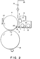
- FIG 2 shows an example of such an image forming apparatus.
- the image forming apparatus comprises a bi-directional emission type LED 1, a photodiode 2, a developing sleeve 3 and an image bearing member in the form of a photosensitive drum 4.
- the developing device 9 is disposed faced to the photosensitive drum 4 and includes a developer chamber 11 and a stirring chamber 12 which are partitioned by a partition wall 10 extending in the direction perpendicular to the sheet of the drawing of Figure 2.
- the portion above the partition wall 10 is opened so as to allow the developer to return from the developer chamber 11 to the stirring chamber by a screw.
- the developer chamber and the stirring chamber 12 contain the two component developer comprising the toner and carrier particles.
- the LED 1 illuminates a test pattern image (patch) 20 which is an area toner image formed on the image bearing member prior to a regular image forming operation.
- the light reflected by the patch 20 is received by a photodiode 2, which produces an electrical output, which is in turn compared with a reference level. In response to the difference between the output and the reference level, the toner is supplied to the upstream side of the screw of the stirring chamber.
- the developer chamber 11 of the developing device 9 is provided with an opening at a position corresponding to a developing zone.
- a developing sleeve 3 is disposed in the opening 14 and is partly exposed to the photosensitive drum 4 in the developing zone.
- the developing sleeve 3 is made of non-magnetic material such as stainless steel or aluminum. During the developing operation, it rotates in a direction indicated by an arrow, and a magnet 13 is stationarily disposed therein to function as a magnetic field generating means.
- the developing sleeve 3 is supplied with an AC biased DC voltage from a voltage source 15, so that the toner is transferred onto the photosensitive drum 4 from the developing sleeve 3 by the electric field of the electrostatic latent image.
- the toner images of different colors are transferred from the photosensitive drum 4 onto the same transfer material carried on the transfer drum 16 by the electric potential produced by the transfer charger 17. After each of the transfer operations, the toner remaining on the drum is cleaned and removed by the cleaning means 18.
- a reference density pattern or patch 20 is formed on the photosensitive drum 4, and the patch 20 is developed under a predetermined developing condition.
- the reflection image density of the developed patch is detected by the photodiode 2, and the detection is used to control the toner content.
- the sensor comprising the LED 1 and the photodiode 2 are easily contaminated by the toner scattered from the developing device 9 with the result of erroneous image density detection and therefore erroneous toner content control.
- an image forming apparatus comprising: an image bearing member movable along an endless path; electrostatic latent image forming means for forming an electrostatic latent image on an image bearing member; developing means for developing the latent image with toner into a toner image; transfer means for transferring the toner image from said image bearing member onto a transfer material, wherein said latent image forming means, said developing means and said transfer means are disposed in the order named with respect to a direction of movement of said image bearing member during image formation; detection pattern image forming means for forming a predetermined pattern image on said image bearing member; detection pattern detecting means, disposed downstream of said transfer means with respect to the movement direction of said image bearing member and disposed faced to said image bearing member, for detecting a state of the detection pattern; and control means for controlling an image forming condition of said image forming apparatus in accordance with a detection by said detecting means.
- Figure 1 is a sectional view of an image forming apparatus according to an embodiment of the present invention.
- Figure 2 is a sectional view of a conventional image forming apparatus.
- Figure 3 is a flow chart of sequential operations of Figure 1 apparatus.
- Figure 4 illustrates a part of an image forming apparatus according to a fifth embodiment of the present invention.
- Figure 5 is a sectional view of the image forming apparatus according to the fifth embodiment of the present invention.
- Figure 6 is a flow chart of sequential operations of the apparatus of the fifth embodiment.
- Figure 7 is a block diagram of a control system for the apparatus according to the fifth embodiment.
- Figure 8 is a flow chart of the sequential operations according to the sixth embodiment of the present invention.
- FIG 1 there is shown an image forming apparatus according to a first embodiment of the present invention.
- the elements 1 - 4, 9 - 18 and 20 are similar to those in Figure 2, and the detailed description thereof are omitted for simplicity.
- the apparatus of Figure 1 includes a pushing means 21, a CPU 22 and a cleaning means 25 for cleaning the transfer drum.
- the LED 1 and the photodiode 2 are disposed downstream of the transfer position where the transfer drum 16 is provided, that is, away from the developing device 9 with the transfer drum 16 disposed therebetween.
- the partition wall 10 is opened at the front and rear sides to provide communication of the developer between the developer chamber 11 and the stirring chamber 12.
- the image forming operation in the image forming apparatus shown in Figure 1, is substantially the same as in the conventional apparatus of Figure 2.
- the CPU 22 produces a signal to prevent generation of the image transfer potential of the transfer charger 17, thus changing the operational state of the transfer charger 17.
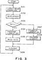
- FIG. 3 shows the sequential operations of this apparatus.
- step S101 an electrostatic latent image of a usual image or a patch pattern is formed by the charger 23 and the light information 24 and is visualized by the developing device 9 at step S102.
- the discrimination is made as to whether the image is the patch pattern or the usual image. If it is the patch, the transfer current to the transfer charger 17 is stopped or reduced at step S104 so as to prevent the patch image from being transferred onto the transfer sheet on the transfer drum 16.
- the patch image is illuminated by the LED 1, and the light reflected thereby is detected by the photodiode 2.
- the output of the photodiode 2 is compared with a reference level. In accordance with the difference from the reference level, the toner is supplied.
- step S106 the toner image of the patch is removed by the cleaning means 18.
- the transfer current is supplied to the transfer charger 17 at step S107 so as to transfer the toner image-onto the transfer material at step S108.
- the patch reading sensor comprising the LED 1 and the photodiode 2 is disposed downstream of the transfer drum 16 with respect to the movement direction of the periphery of the image bearing member.
- the charge of the transfer drum 16 is removed, or it is charged to the polarity which is the same as the toner charge, when the patch 20 passes on the transfer drum 16.
- the patch image is stably read without contamination of the sensor surfaces.
- the pushing means 21 in the form of a sheet made of polyethylene or a rod pushes the transfer material supporting sheet of the transfer drum 16 to provide the proper nip pressure.
- the pushing means 21 is released when the patch 20 passes by the transfer drum to prevent the transfer of the patch image to the transfer drum or the transfer material thereon. For the purpose of this release, the pushing means 21 is rotated or moved.
- the voltage applied to the transfer charger during rotation of the photosensitive drum is opposite when the usual image is at the transfer position from that when the patch image 20 is at the transfer position.
- the used toner is charged to the negative polarity, and therefore, the potential of the transfer drum is positive when the usual toner image is to be transferred onto the transfer material.
- the negative potential is produced.
- Embodiment 3 may be combined with Embodiment 2.
- the sensor comprises an LED 1 and a photodiode 2 which are disposed at the opposite side of the developing device 9 from the transfer drum 16.
- the density detecting patch includes 16 tone gradation levels formed at predetermined timing and is used as information for controlling image forming conditions. On the basis of the detection, a relation between an input pulse and output density, is determined. Then, a tone gradation correcting function (LUT ... look-up table) is determined. Using the correction function LUT, the image forming condition or conditions are changed. Examples of the image forming conditions include the degree of charging, the exposure amount, the level of developing bias, the transfer bias and a combination of them.
- the density detecting means for detecting the toner image formed on the photosensitive member is disposed at an opposite side of the transfer means from the developing means. Therefore, the contamination of the detecting surface or surfaces of the density detecting means can be prevented from being contaminated with the toner, and therefore, the density detecting operation is stabilized.
- the transfer bias voltage application is changed so as to prevent the toner image during the patch detecting operation, when the transfer drum is used. Therefore, the transfer drum is also prevented from contamination.
- the present invention is effective when the transfer drum is replaced with an intermediate image transfer material or a transfer material conveying belt.
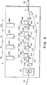
- the image forming apparatus of this embodiment is capable of forming color images and comprises plural image forming stations.
- Figure 4 shows only one of such stations, and
- Figure 5 shows all of the stations.
- the image forming apparatus is shown as being of a laser beam printer type and comprises four photosensitive drums 26M, 26C, 26Y and 26K and optical scanning means therefor using plural laser beams.
- the number of image forming stations corresponds to the number of colors.
- the toner image on the photosensitive drum formed at each of the image forming stations is transferred onto the transfer drum conveyed on a transfer belt 31a to face the transfer material to the photosensitive drums sequentially.
- the image forming stations Pm, Pc, Py and Pk are for magenta, cyan, yellow and black colors, respectively, and are provided with the photosensitive drums 26M, 26C, 26Y and 26K, respectively.
- the photosensitive drums are rotated in the direction indicated by arrows (clockwise direction).
- a primary (corona) charger 27M, 27C, 27Y or 27K there are a primary (corona) charger 27M, 27C, 27Y or 27K, optical scanning means 28M, 28C, 28Y or 28K, a developing device 29M, 29C, 29Y or 29K, and a cleaning device 30M, 30C, 30Y or 30K.
- An image transfer means 31 constituting image forming means comprises a transfer belt 31a common to all of the image forming stations, transfer chargers 31M, 31C, 31Y and 31K for the respective transfer stations.
- the transfer material P conveyed in the predetermined direction on the transfer drum 31a receives sequentially the toner images of the different colors from the photosensitive drum.
- Polyethylene sheets 41M, 41C, 41Y and 41K are disposed below the photosensitive drums 26M, 26C, 26Y and 26K, respectively to provide the proper nip pressure between the photosensitive drum and the transfer belt 31a, that is, the transfer belt 31a is pushed upwardly by the sheets.
- the sheets are rotatable to take contact and non-contact positions, thus permitting contact and non-contact between the photosensitive drum and the transfer belt.
- the transfer material P is supplied from a sheet feeding cassette 38, and the transfer material P after being subjected to the transfer step is separated from the photosensitive drum and is discharged onto a tray 40 after being subjected to an image fixing operation of a fixing device 39.
- the scanning optical means 28M, 28C, 28Y and 28K each include a laser source not shown, a rotatable polygonal mirror for scanning the laser beam from the laser source, an f-0lens for condensing the scanning beam on the photosensitive drum surface along a generating line direction of the photosensitive drum, a reflecting mirror for deflecting the beam and a beam detector for detecting a predetermined position of the scanning beam.
- Figure 4 shows an enlarged view of a fourth station in which the image is developed with black toner.
- the other three stations have the similar structure.
- FIG 4 there is shown a potential sensor 42K to detect the surface potential of the photosensitive drum 26K.
- a potentiometer 45 is connected with the potential sensor 42.
- the potentiometer 45 is connected to a controller 46, and the surface potential information on the photosensitive drum 26K is transmitted to a controller 46.
- a developer content sensor 44 is provided so as to properly supply the toner. More particularly, the toner is supplied in accordance with a signal produced from a developer content sensor 44 to maintain a constant developer content in the developing device 29K, the developer content being determined by the ratio of the toner and the carrier.
- the known developer content sensor is of light reflection type, an inductance type, a patch detection type or the like. The information of the developer content sensor 44 is transmitted to the controller 46.
- a test patch 47 which is a pattern formed on the photosensitive drum to permit detection of the toner density, and is transferred onto the transfer belt 31a as a visualized image. It may be a step patch having 8 or 16 different tone gradation levels from the minimum density level to the maximum density level, or may be a single density level patch.
- the test patch pattern is formed as a latent image on the photosensitive drum by a test pattern generator, and is visualized by the developing device 29K.
- a patch image density sensor 43 function as the density detecting means and is disposed at an opposite side of the transfer station from the developing device 29K, An output of the patch image density sensor 42K is supplied to the controller 46.
- the controller 46 also functions to control the scanning optical system 28K so as to change the quantity of the laser light to provide proper image forming conditions in accordance with the potential information, the developer density information and the patch density information.
- the material of the transfer belt 31a may be polyurethane material, polycarbonate material, PVdF (polyvinylidene fluoride) or the like.
- the toner has an average particle size of 3 - 20 microns and comprises polyester resin and coloring pigments dispersed therein.
- the toner powder contains silica particles.
- the materials may be styrene-acryl resin material, and the coloring material may be carbon black, benzene yellow pigment, anthraquinone dye, copper phthalocyanine pigment.
- the transfer efficiency is determined on the basis of the density of the test patch pattern 47, and on the basis of the determination, the image density is stabilised.
- the test patch latent image is formed on each of the photosensitive drums 26M, 26C, 26Y and 26K.
- the test patch comprises 8 bit linear density levels from 00 (white) to FF (black), and therefore, the test patch latent image is expressed as FFH.
- the latent images are visualised by the developing devices 29M, 29C, 29Y and 29K, respectively.
- the pushing films 41M, 41C, 41Y and 41K are placed at a non-contact position relative to the transfer belt 31a, so that the transfer belt 31a is spaced from the photosensitive drum.
- the image density of the test patch pattern is optically detected and converted to an electric signal by the patch image density sensor 43.
- the photosensitive drum is cleaned so that the residual toner is removed.
- test patch latent image is formed in the same manner as with step S101.
- latent image is visualised in the same manner as in step S102.
- the pushing sheets 41M, 41C, 41Y and 41K are moved to the upward position to cause the transfer belt 31a to contact the photosensitive drum, and transfer currents are applied to the transfer chargers 31M, 31C, 31Y and 31K when the test patch patterns 47 are in the respective image transfer stations, so that the test patch patterns 47 are transferred onto the transfer belt 31a by the image transfer potential provided at the image transfer stations.
- the patch density sensors 43 detect the image densities of the test patches 47 remaining on the photosensitive drum 26M, 26C, 26Y and 26K.
- the test patch patterns 47 on the photosensitive drum 26M, 26C, 26Y and 26K are removed by the cleaners 30M, 30C, 30Y and 30K, and the test patch pattern toners on the transfer belt 31a are removed by unshown belt cleaners.
- the pre-transfer density Da determined at step S104 and the post-transfer density Db determined at S109 are subjected to the transfer efficiency calculation.
- the image forming condition or conditions are controlled on the basis of the transfer efficiency thus obtained.
- the pre-transfer density Da and the post-transfer density Db are converted to digital signals by A/D converter means and are transmitted to the controller 46, where the transfer efficiency (1-Db)/Da % is determined.
- the following discrimination is carried out. On the basis of the signal from the potential sensor 42, the discrimination is made as to whether the developing contrast potential or the like depending on the charger 27K intended by the controller 46 is correctly provided or not. If not, the following transfer current control is prevented by producing error message or the like.
- the discrimination is made as to whether the toner content T/(T+C) (wt. %) is deviated from the reference density or not, on the basis of the output of the developer density sensor 44. If it is not deviated, the following transfer current control is carried out.
- the results of the detections by the patch image density sensor 42, the potential sensor 42 and the developer density sensor 44 are discriminated by the controller 46. If the transfer efficiency is deviated from 85 ⁇ 5 %, the controller 46 produces instruction to the transfer current control circuit 48 in accordance with the deviation so as to provide the proper transfer efficiency.
- one patch image density sensor disposed at a side of the transfer position from the developing device is enough to determine the transfer efficiency, and therefore, to properly control the image forming condition.
- two image forming operation processes are carried out to form the test patch images for determinations of the pre-transfer image density and the post-transfer image density, respectively.
- the transfer efficiency is calculated and controlled.
- the transfer efficiency is calculated and controlled through one image forming process.
- the transfer drum is rotatable in the opposite direction.
- the latent images of the test patches FFH are formed on the photosensitive drums 26M, 26C, 26Y and 26K.
- the latent images are visualized by the developing devices 29M, 29C, 29Y and 29K.
- the pushing films 41M, 41C, 41Y and 41K are spaced away from the belt 31a to bring the transfer belt 31a out of contact with the drum, so that the test patch 47 passes through the image transfer station while being out of contact with the transfer belt 31a.
- the test patch 47 becomes faced to the patch image density sensor 43M, 43C, 43Y or 43K, the image density is detected. Then, the photosensitive drum 26M, 26C, 26Y or 26K is stopped.
- the photosensitive drums 26M, 26C, 26Y and 26K are rotated in the opposite direction, and the photosensitive drums are then stopped when the test images are at the positions between the transfer belt 31a and the associated developing devices 29M, 29C, 29Y and 29K.
- the films 41M, 41C, 41Y and 41K are contacted to the belt 31a.
- the photosensitive drums are rotated in the forward direction, again.
- the test patches 47 passes through the transfer position (transfer belt 31a)
- the image transfer current is supplied to the transfer chargers 31M, 31C, 31Y and 31K, so that the transfer voltages are applied, and therefore, the test patches 47 are transferred onto the transfer belt.
- the image densities of the test patches 43a remaining on the associated photosensitive drums 26M, 26C, 26Y and 26K are detected at step S109 by the patch density sensors 43M, 43C, 43Y and 43K. Thereafter, the images are removed by the cleaning means at step S110. Similarly to the fifth embodiment, the transfer efficiency is calculated at step S111.
- the pre-transfer and post-transfer image densities can be detected through one test patch image formation.
- the image forming condition is controlled on the basis of the transfer efficiency and other factors including the maximum image density Dmax, a highlight reproducibility, tone gradation linearity or the like, so that a higher precision control is accomplished.
- densities of a predetermined pattern on the photosensitive drums 26M, 26C, 26Y and 26K are detected, and on the basis of the detections, the development contrast potential (the difference between the developing bias and the light potential) and the difference between the developing bias and the dark potential, are changed to stabilize the maximum image density Dmax and the highlight reproducibility.
- tone gradation pattern is formed on the each of the photosensitive drums 26M, 26C, 26Y and 26K.
- the LUT tone gradation correcting look-up table
- the transfer efficiency is controlled through the steps as in the fourth or fifth embodiments, so that the image quality is stabilized.
- the combination with the other image stabilising means is effective to stabilize the formed image.
- the density detecting means for detecting the image density of the pattern and the means for forming the pattern for the image density detection on the image bearing member are disposed only at an opposite side of the transfer position from the developing means. On the basis of the detection, the image transfer efficiency is determined. On the basis of the determination in turn, the image forming condition or conditions are controlled properly.
- the number of density detection sensors is the minimum, and therefore, the transferred image can be stabilized without increasing required space and cost.
Abstract
Description
- The present invention relates to an image forming apparatus having an image forming condition controller responsive to a test pattern image, more particularly to an image forming apparatus in which a test pattern is formed on an image bearing member such as an electrophotographic photosensitive member, and an image forming condition is controlled in accordance with detection of the test pattern. Various types of full-color image forming machines have been proposed, including an electrophotographic type, an ink jet recording type or a thermal transfer recording type. Among them, the electrophotographic type is advantageous in the high speed printing and availability of the plain paper, and therefore, the developments thereof are promoted.
- In the electrophotographic type full-color image forming machines, the developing device is two-component developer type using two component developer including toner and magnetic carrier particles, from the standpoint of the color balance of the image or the like. In the developing device, when the toner in the developing device is consumed by the image forming operation, the toner is supplied into the developing device to compensate for the consumption of the toner. In order to accomplish this, the developer content detector and the control device are used to maintain the toner content.
- Figure 2 shows an example of such an image forming apparatus. The image forming apparatus comprises a bi-directional emission type LED 1, a
photodiode 2, a developingsleeve 3 and an image bearing member in the form of aphotosensitive drum 4. The developingdevice 9 is disposed faced to thephotosensitive drum 4 and includes adeveloper chamber 11 and astirring chamber 12 which are partitioned by apartition wall 10 extending in the direction perpendicular to the sheet of the drawing of Figure 2. The portion above thepartition wall 10 is opened so as to allow the developer to return from thedeveloper chamber 11 to the stirring chamber by a screw. - The developer chamber and the
stirring chamber 12 contain the two component developer comprising the toner and carrier particles. The LED 1 illuminates a test pattern image (patch) 20 which is an area toner image formed on the image bearing member prior to a regular image forming operation. The light reflected by thepatch 20 is received by aphotodiode 2, which produces an electrical output, which is in turn compared with a reference level. In response to the difference between the output and the reference level, the toner is supplied to the upstream side of the screw of the stirring chamber. - The
developer chamber 11 of the developingdevice 9 is provided with an opening at a position corresponding to a developing zone. A developingsleeve 3 is disposed in theopening 14 and is partly exposed to thephotosensitive drum 4 in the developing zone. The developingsleeve 3 is made of non-magnetic material such as stainless steel or aluminum. During the developing operation, it rotates in a direction indicated by an arrow, and amagnet 13 is stationarily disposed therein to function as a magnetic field generating means. When the developing operation is carried out to visualize the latent image on thephotosensitive drum 4, the developingsleeve 3 is supplied with an AC biased DC voltage from avoltage source 15, so that the toner is transferred onto thephotosensitive drum 4 from the developingsleeve 3 by the electric field of the electrostatic latent image. - The toner images of different colors are transferred from the
photosensitive drum 4 onto the same transfer material carried on thetransfer drum 16 by the electric potential produced by thetransfer charger 17. After each of the transfer operations, the toner remaining on the drum is cleaned and removed by the cleaning means 18. - Thus, a reference density pattern or
patch 20 is formed on thephotosensitive drum 4, and thepatch 20 is developed under a predetermined developing condition. The reflection image density of the developed patch is detected by thephotodiode 2, and the detection is used to control the toner content. - However, in the conventional example shown in Figure 2, the sensor comprising the LED 1 and the
photodiode 2 are easily contaminated by the toner scattered from the developingdevice 9 with the result of erroneous image density detection and therefore erroneous toner content control. - Accordingly, it is a principal object of the present invention to provide an image forming apparatus in which the detecting means for detecting the test pattern on the image bearing member is prevented from contamination with the scattered toner so as to maintain the correct control on the basis of the detection.
- It is a further object of the present invention to provide an image forming apparatus in which the toner image is detected so that the result of the development is used to control an image forming condition, so that the control accuracy is improved.
- According to an aspect of the present invention, there is provided an image forming apparatus, comprising: an image bearing member movable along an endless path; electrostatic latent image forming means for forming an electrostatic latent image on an image bearing member; developing means for developing the latent image with toner into a toner image; transfer means for transferring the toner image from said image bearing member onto a transfer material, wherein said latent image forming means, said developing means and said transfer means are disposed in the order named with respect to a direction of movement of said image bearing member during image formation; detection pattern image forming means for forming a predetermined pattern image on said image bearing member; detection pattern detecting means, disposed downstream of said transfer means with respect to the movement direction of said image bearing member and disposed faced to said image bearing member, for detecting a state of the detection pattern; and control means for controlling an image forming condition of said image forming apparatus in accordance with a detection by said detecting means.
- These and other objects, features and advantages of the present invention will become more apparent upon a consideration of the following description of the preferred embodiments of the present invention taken in conjunction with the accompanying drawings.
- Figure 1 is a sectional view of an image forming apparatus according to an embodiment of the present invention.
- Figure 2 is a sectional view of a conventional image forming apparatus.
- Figure 3 is a flow chart of sequential operations of Figure 1 apparatus.
- Figure 4 illustrates a part of an image forming apparatus according to a fifth embodiment of the present invention.
- Figure 5 is a sectional view of the image forming apparatus according to the fifth embodiment of the present invention.
- Figure 6 is a flow chart of sequential operations of the apparatus of the fifth embodiment.
- Figure 7 is a block diagram of a control system for the apparatus according to the fifth embodiment.
- Figure 8 is a flow chart of the sequential operations according to the sixth embodiment of the present invention.
- Referring to Figure 1, there is shown an image forming apparatus according to a first embodiment of the present invention. In Figure 1, the elements 1 - 4, 9 - 18 and 20 are similar to those in Figure 2, and the detailed description thereof are omitted for simplicity. The apparatus of Figure 1 includes a pushing means 21, a
CPU 22 and a cleaning means 25 for cleaning the transfer drum. - In this embodiment, as shown in Figure 1 the LED 1 and the
photodiode 2 are disposed downstream of the transfer position where thetransfer drum 16 is provided, that is, away from the developingdevice 9 with thetransfer drum 16 disposed therebetween. Although not shown, thepartition wall 10 is opened at the front and rear sides to provide communication of the developer between thedeveloper chamber 11 and thestirring chamber 12. - The image forming operation in the image forming apparatus shown in Figure 1, is substantially the same as in the conventional apparatus of Figure 2. However, when the test pattern or
patch 20 for the toner content control is developed by the developingdevice 9, theCPU 22 produces a signal to prevent generation of the image transfer potential of thetransfer charger 17, thus changing the operational state of thetransfer charger 17. - Figure 3 shows the sequential operations of this apparatus. At step S101, an electrostatic latent image of a usual image or a patch pattern is formed by the
charger 23 and thelight information 24 and is visualized by the developingdevice 9 at step S102. - At step S103, the discrimination is made as to whether the image is the patch pattern or the usual image. If it is the patch, the transfer current to the
transfer charger 17 is stopped or reduced at step S104 so as to prevent the patch image from being transferred onto the transfer sheet on thetransfer drum 16. At step S105, the patch image is illuminated by the LED 1, and the light reflected thereby is detected by thephotodiode 2. The output of thephotodiode 2 is compared with a reference level. In accordance with the difference from the reference level, the toner is supplied. - At step S106, the toner image of the patch is removed by the cleaning means 18.
- If the discrimination at step S103 indicates that the image is the usual image, the transfer current is supplied to the
transfer charger 17 at step S107 so as to transfer the toner image-onto the transfer material at step S108. - As will be understood, the patch reading sensor comprising the LED 1 and the
photodiode 2 is disposed downstream of thetransfer drum 16 with respect to the movement direction of the periphery of the image bearing member. When thepatch 20 passes on thetransfer drum 16, the charge of thetransfer drum 16 is removed, or it is charged to the polarity which is the same as the toner charge, when thepatch 20 passes on thetransfer drum 16. By doing so, the patch image is stably read without contamination of the sensor surfaces. - When the usual toner image is transferred from the
photosensitive drum 4 onto the transfer material on thetransfer drum 16, the pushing means 21 in the form of a sheet made of polyethylene or a rod pushes the transfer material supporting sheet of thetransfer drum 16 to provide the proper nip pressure. In this embodiment, thepushing means 21 is released when thepatch 20 passes by the transfer drum to prevent the transfer of the patch image to the transfer drum or the transfer material thereon. For the purpose of this release, the pushingmeans 21 is rotated or moved. - In this embodiment, the voltage applied to the transfer charger during rotation of the photosensitive drum is opposite when the usual image is at the transfer position from that when the
patch image 20 is at the transfer position. - For example, the used toner is charged to the negative polarity, and therefore, the potential of the transfer drum is positive when the usual toner image is to be transferred onto the transfer material. In this case, when the
patch image 20 passes by thetransfer drum 16, the negative potential is produced. -
Embodiment 3 may be combined withEmbodiment 2. - In this embodiment, the sensor comprises an LED 1 and a
photodiode 2 which are disposed at the opposite side of the developingdevice 9 from thetransfer drum 16. The density detecting patch includes 16 tone gradation levels formed at predetermined timing and is used as information for controlling image forming conditions. On the basis of the detection, a relation between an input pulse and output density, is determined. Then, a tone gradation correcting function (LUT ... look-up table) is determined. Using the correction function LUT, the image forming condition or conditions are changed. Examples of the image forming conditions include the degree of charging, the exposure amount, the level of developing bias, the transfer bias and a combination of them. - According to the embodiments 1 - 4, the density detecting means for detecting the toner image formed on the photosensitive member, is disposed at an opposite side of the transfer means from the developing means. Therefore, the contamination of the detecting surface or surfaces of the density detecting means can be prevented from being contaminated with the toner, and therefore, the density detecting operation is stabilized.
- The transfer bias voltage application is changed so as to prevent the toner image during the patch detecting operation, when the transfer drum is used. Therefore, the transfer drum is also prevented from contamination. The present invention is effective when the transfer drum is replaced with an intermediate image transfer material or a transfer material conveying belt.
- Referring to Figures 4 and 5, the description will first be made as to the general arrangement of an image forming apparatus according to a fifth embodiment.
- The image forming apparatus of this embodiment is capable of forming color images and comprises plural image forming stations. Figure 4 shows only one of such stations, and Figure 5 shows all of the stations.
- Referring to Figure 5, the image forming apparatus is shown as being of a laser beam printer type and comprises four
photosensitive drums - There are four image forming stations each having the electrophotographic photosensitive member each of the photosensitive drum. The number of image forming stations corresponds to the number of colors. The toner image on the photosensitive drum formed at each of the image forming stations is transferred onto the transfer drum conveyed on a
transfer belt 31a to face the transfer material to the photosensitive drums sequentially. - The image forming stations Pm, Pc, Py and Pk are for magenta, cyan, yellow and black colors, respectively, and are provided with the
photosensitive drums photosensitive drum charger device cleaning device - An image transfer means 31 constituting image forming means comprises a
transfer belt 31a common to all of the image forming stations,transfer chargers transfer drum 31a, receives sequentially the toner images of the different colors from the photosensitive drum.Polyethylene sheets photosensitive drums transfer belt 31a, that is, thetransfer belt 31a is pushed upwardly by the sheets. The sheets are rotatable to take contact and non-contact positions, thus permitting contact and non-contact between the photosensitive drum and the transfer belt. - The transfer material P is supplied from a
sheet feeding cassette 38, and the transfer material P after being subjected to the transfer step is separated from the photosensitive drum and is discharged onto atray 40 after being subjected to an image fixing operation of a fixingdevice 39. - The scanning
optical means - Figure 4 shows an enlarged view of a fourth station in which the image is developed with black toner. The other three stations have the similar structure.
- In Figure 4, there is shown a
potential sensor 42K to detect the surface potential of thephotosensitive drum 26K. Apotentiometer 45 is connected with thepotential sensor 42. Thepotentiometer 45 is connected to acontroller 46, and the surface potential information on thephotosensitive drum 26K is transmitted to acontroller 46. Adeveloper content sensor 44 is provided so as to properly supply the toner. More particularly, the toner is supplied in accordance with a signal produced from adeveloper content sensor 44 to maintain a constant developer content in the developingdevice 29K, the developer content being determined by the ratio of the toner and the carrier. The known developer content sensor is of light reflection type, an inductance type, a patch detection type or the like. The information of thedeveloper content sensor 44 is transmitted to thecontroller 46. - A
test patch 47 which is a pattern formed on the photosensitive drum to permit detection of the toner density, and is transferred onto thetransfer belt 31a as a visualized image. It may be a step patch having 8 or 16 different tone gradation levels from the minimum density level to the maximum density level, or may be a single density level patch. The test patch pattern is formed as a latent image on the photosensitive drum by a test pattern generator, and is visualized by the developingdevice 29K. - A patch
image density sensor 43 function as the density detecting means and is disposed at an opposite side of the transfer station from the developingdevice 29K, An output of the patchimage density sensor 42K is supplied to thecontroller 46. Thecontroller 46 also functions to control the scanningoptical system 28K so as to change the quantity of the laser light to provide proper image forming conditions in accordance with the potential information, the developer density information and the patch density information. - The material of the
transfer belt 31a may be polyurethane material, polycarbonate material, PVdF (polyvinylidene fluoride) or the like. In this embodiment, the toner has an average particle size of 3 - 20 microns and comprises polyester resin and coloring pigments dispersed therein. The toner powder contains silica particles. Depending on the colors, the materials may be styrene-acryl resin material, and the coloring material may be carbon black, benzene yellow pigment, anthraquinone dye, copper phthalocyanine pigment. - In this apparatus, the transfer efficiency is determined on the basis of the density of the
test patch pattern 47, and on the basis of the determination, the image density is stabilised. - Referring to Figure 6, the operation will be described in detail. At step S101, the test patch latent image is formed on each of the
photosensitive drums devices films transfer belt 31a, so that thetransfer belt 31a is spaced from the photosensitive drum. At step S104, the image density of the test patch pattern is optically detected and converted to an electric signal by the patchimage density sensor 43. At step S105, the photosensitive drum is cleaned so that the residual toner is removed. - At step S106, the test patch latent image is formed in the same manner as with step S101. At step S107, the latent image is visualised in the same manner as in step S102.
- At step S108, the pushing
sheets transfer belt 31a to contact the photosensitive drum, and transfer currents are applied to thetransfer chargers test patch patterns 47 are in the respective image transfer stations, so that thetest patch patterns 47 are transferred onto thetransfer belt 31a by the image transfer potential provided at the image transfer stations. - At step S109, the
patch density sensors 43 detect the image densities of thetest patches 47 remaining on thephotosensitive drum test patch patterns 47 on thephotosensitive drum cleaners transfer belt 31a are removed by unshown belt cleaners. - The pre-transfer density Da determined at step S104 and the post-transfer density Db determined at S109 are subjected to the transfer efficiency calculation. The image forming condition or conditions are controlled on the basis of the transfer efficiency thus obtained.
- Referring to Figure 7, the description will be made as to the control. The pre-transfer density Da and the post-transfer density Db are converted to digital signals by A/D converter means and are transmitted to the
controller 46, where the transfer efficiency
- In parallel with the above-operation, the following discrimination is carried out. On the basis of the signal from the
potential sensor 42, the discrimination is made as to whether the developing contrast potential or the like depending on thecharger 27K intended by thecontroller 46 is correctly provided or not. If not, the following transfer current control is prevented by producing error message or the like. - If so, the discrimination is made as to whether the toner content

developer density sensor 44. If it is not deviated, the following transfer current control is carried out. - The results of the detections by the patch
image density sensor 42, thepotential sensor 42 and thedeveloper density sensor 44 are discriminated by thecontroller 46. If the transfer efficiency is deviated from 85 ± 5 %, thecontroller 46 produces instruction to the transfercurrent control circuit 48 in accordance with the deviation so as to provide the proper transfer efficiency. - In this manner, one patch image density sensor disposed at a side of the transfer position from the developing device is enough to determine the transfer efficiency, and therefore, to properly control the image forming condition.
- The fundamental structures of the apparatus of this embodiment are the same as in the fifth embodiment, and therefore, the description will be made particularly as to the different portions.
- In the fifth embodiment, two image forming operation processes are carried out to form the test patch images for determinations of the pre-transfer image density and the post-transfer image density, respectively. On the basis of the image density difference, the transfer efficiency is calculated and controlled. In this embodiment, the transfer efficiency is calculated and controlled through one image forming process. The transfer drum is rotatable in the opposite direction.
- Referring to Figure 8, the operation will be described. At step S101, the latent images of the test patches FFH are formed on the
photosensitive drums devices films belt 31a to bring thetransfer belt 31a out of contact with the drum, so that thetest patch 47 passes through the image transfer station while being out of contact with thetransfer belt 31a. When thetest patch 47 becomes faced to the patchimage density sensor 43M, 43C, 43Y or 43K, the image density is detected. Then, thephotosensitive drum - At step S105, the
photosensitive drums transfer belt 31a and the associated developingdevices films belt 31a. Then, at step S108, the photosensitive drums are rotated in the forward direction, again. When thetest patches 47 passes through the transfer position (transferbelt 31a), the image transfer current is supplied to thetransfer chargers test patches 47 are transferred onto the transfer belt. The image densities of the test patches 43a remaining on the associatedphotosensitive drums patch density sensors 43M, 43C, 43Y and 43K. Thereafter, the images are removed by the cleaning means at step S110. Similarly to the fifth embodiment, the transfer efficiency is calculated at step S111. - According to this embodiment, the pre-transfer and post-transfer image densities can be detected through one test patch image formation.
- In this embodiment, the image forming condition is controlled on the basis of the transfer efficiency and other factors including the maximum image density Dmax, a highlight reproducibility, tone gradation linearity or the like, so that a higher precision control is accomplished. As a first step, densities of a predetermined pattern on the
photosensitive drums photosensitive drums step 3, the transfer efficiency is controlled through the steps as in the fourth or fifth embodiments, so that the image quality is stabilized. - As described, the combination with the other image stabilising means is effective to stabilize the formed image.
- As described in the foregoing, according to the Embodiments 5 - 7, the density detecting means for detecting the image density of the pattern and the means for forming the pattern for the image density detection on the image bearing member, are disposed only at an opposite side of the transfer position from the developing means. On the basis of the detection, the image transfer efficiency is determined. On the basis of the determination in turn, the image forming condition or conditions are controlled properly.
- In the embodiments, the number of density detection sensors is the minimum, and therefore, the transferred image can be stabilized without increasing required space and cost.
- While the invention has been described with reference to the structures disclosed herein, it is not confined to the details set forth and this application is intended to cover such modifications or changes as may come within the purposes of the improvements or the scope of the following claims.
Claims (17)
- An image forming apparatus, comprising:
an image bearing member movable along an endless path;
electrostatic latent image forming means for forming an electrostatic latent image on an image bearing member;
developing means for developing the latent image with toner into a toner image;
transfer means for transferring the toner image from said image bearing member onto a transfer material, wherein said latent image forming means, said developing means and said transfer means are disposed in the order named with respect to a direction of movement of said image bearing member during image formation;
detection pattern image forming means for forming a predetermined pattern image on said image bearing member;
detection pattern detecting means, disposed downstream of said transfer means with respect to the movement direction of said image bearing member and disposed faced to said image bearing member, for detecting a state of the detection pattern; and
control means for controlling an image forming condition of said image forming apparatus in accordance with a detection by said detecting means. - An apparatus according to Claim 1, wherein said detecting means forms a predetermined shaped toner image using said latent image forming means and said developing means.
- An apparatus according to Claim 1, wherein said detecting means includes a light source and a photoreceptor.
- An image forming apparatus, comprising:
an image bearing member movable along an endless path;
electrostatic latent image forming means for forming an electrostatic latent image on an image bearing member;
developing means for developing the latent image with toner into a toner image;
transfer means for transferring the toner image from said image bearing member onto a transfer material, wherein said latent image forming means, said developing means and said transfer means are disposed in the order named with respect to a direction of movement of said image bearing member during image formation;
detection pattern image forming means for forming a predetermined pattern image on said image bearing member;
detection pattern detecting means, disposed downstream of said transfer means with respect to the movement direction of said image bearing member and disposed faced to said image bearing member, for detecting a state of the detection pattern;
control means for controlling an image forming condition of said image forming apparatus in accordance with a detection of said detecting means;
transfer operation control means for controlling said transfer means when the detection pattern passes through an image transfer position where said transfer means is disposed. - An apparatus according to Claim 4, wherein said transfer operation control means stops a bias voltage to said transfer means when the detection pattern passes through the transfer position.
- An apparatus according to Claim 4, wherein said transfer operation control means supplies to said transfer means a voltage having a polarity opposite from that during usual image transfer operation.
- An apparatus according to Claim 4, wherein said detecting means includes a light source and a photoreceptor.
- An apparatus according to Claim 4, wherein said image forming condition control means controls a transfer bias applied to said transfer means.
- An apparatus according to Claim 4, wherein said image forming condition control means controls a potential of the latent image formed by said latent image forming means.
- An apparatus according to Claim 4, wherein said image forming condition control means-controls said developing means.
- An image forming apparatus, comprising:
an image bearing member movable along an endless path;
electrostatic latent image forming means for forming an electrostatic latent image on an image bearing member;
developing means for developing the latent image with toner into a toner image;
transfer means for transferring the toner image from said image bearing member onto a transfer material, wherein said latent image forming means, said developing means and said transfer means are disposed in the order named with respect to a direction of movement of said image bearing member during image formation;
detection pattern image forming means for forming a predetermined pattern image on said image bearing member;
detection pattern detecting means, disposed downstream of said transfer means with respect to the movement direction of said image bearing member and disposed faced to said image bearing member, for detecting a state of the detection pattern, wherein said detecting means detects the state before and after the detection pattern is transferred-by said transfer means;
control means for controlling an image forming condition of said image forming apparatus in accordance with a detection of said detecting means; and
transfer operation control means for controlling said transfer means when the detection pattern passes through an image transfer position where said image transfer means is disposed. - An apparatus according to Claim 11, wherein said image bearing member is rotatable in a direction opposite from that during image formation to permit the detection of said detecting means before and after the detection pattern is transferred, by which the states are detected by one detecting means.
- Image forming apparatus in which an electrical image is formed on an image bearing member, the electrical image is developed into a toner image at a developing means, and the toner image is transferred to an image support means at a transfer means, the apparatus having means to form a test image on the image bearing member and means to detect the test image,
characterised in that the means to detect the test image is downstream of the transfer means. - Image forming apparatus according to claim 13 in which the transfer means is operable in a transfer mode to transfer a toner image from the image bearing member to the image support means, and is operable in a non-transfer mode to allow the test image to pass without transferring it to the image support means.
- A method of operating an image forming apparatus in a test mode, in which a test image is formed on an image bearing member, and is detected by detection means, the test image being carried past an image transfer means for transferring images to another means,
characterised by the step of maintaining the image transfer means in a mode for not transferring images while the test image is carried past it. - A method of operating an image forming apparatus in a test mode, in which a test image is formed on an image bearing member and is detected by detection means,
characterised in that
the test image is transferred to another means subsequent to its detection by the detection means, and the location of the test image on the image bearing means is subsequently sensed, the location of the test image not being cleaned between the test image detection step and the location sensing step. - A method according to claim 16 in which the image bearing member is moved in a forward direction between the step of forming the test image and the step of detecting the test image, and is moved in a reverse direction between the step of detecting the test image and the step of sensing the location.
Applications Claiming Priority (4)
| Application Number | Priority Date | Filing Date | Title |
|---|---|---|---|
| JP14620091 | 1991-06-18 | ||
| JP146200/91 | 1991-06-18 | ||
| JP198929/91 | 1991-07-12 | ||
| JP19892991 | 1991-07-12 |
Publications (3)
| Publication Number | Publication Date |
|---|---|
| EP0519710A2 true EP0519710A2 (en) | 1992-12-23 |
| EP0519710A3 EP0519710A3 (en) | 1993-02-24 |
| EP0519710B1 EP0519710B1 (en) | 1996-08-21 |
Family
ID=26477083
Family Applications (1)
| Application Number | Title | Priority Date | Filing Date |
|---|---|---|---|
| EP19920305567 Expired - Lifetime EP0519710B1 (en) | 1991-06-18 | 1992-06-17 | Image forming apparatus having image forming condition controller responsive to test pattern image |
Country Status (2)
| Country | Link |
|---|---|
| EP (1) | EP0519710B1 (en) |
| DE (1) | DE69212915T2 (en) |
Cited By (6)
| Publication number | Priority date | Publication date | Assignee | Title |
|---|---|---|---|---|
| EP0740222A2 (en) * | 1995-04-28 | 1996-10-30 | Canon Kabushiki Kaisha | White electroconductive coating composition and transfer material-carrying member |
| US5581327A (en) * | 1993-12-28 | 1996-12-03 | Canon Kabushiki Kaisha | Image forming apparatus |
| WO1999034260A1 (en) * | 1997-12-29 | 1999-07-08 | Eastman Kodak Company | Image forming apparatus and method with control of electrostatic transfer using constant current |
| EP2053466A2 (en) | 2007-10-23 | 2009-04-29 | Ricoh Company, Ltd. | Image forming apparatus and developer supply method therefor |
| CN101261474B (en) * | 2007-03-06 | 2010-06-16 | 夏普株式会社 | Image forming apparatus |
| US7845788B2 (en) | 2006-08-28 | 2010-12-07 | Fujifilm Corporation | Image forming apparatus and method |
Citations (6)
| Publication number | Priority date | Publication date | Assignee | Title |
|---|---|---|---|---|
| DE3220993A1 (en) * | 1981-06-08 | 1982-12-23 | Minolta Camera K.K., Osaka | ELECTROPHOTOGRAPHIC COPIER |
| JPS59123857A (en) * | 1982-12-29 | 1984-07-17 | Canon Inc | Image reproduction controlling device |
| JPS6155675A (en) * | 1984-08-27 | 1986-03-20 | Fujitsu Ltd | Transfer type printer |
| US4797705A (en) * | 1986-02-04 | 1989-01-10 | Minolta Camera Kabushiki Kaisha | Image forming apparatus having a high-voltage unit malfunction detecting function |
| EP0323226A2 (en) * | 1987-12-28 | 1989-07-05 | Canon Kabushiki Kaisha | An image forming apparatus |
| GB2212419A (en) * | 1987-12-25 | 1989-07-26 | Ricoh Kk | Controlling image density in colour copiers |
-
1992
- 1992-06-17 DE DE1992612915 patent/DE69212915T2/en not_active Expired - Lifetime
- 1992-06-17 EP EP19920305567 patent/EP0519710B1/en not_active Expired - Lifetime
Patent Citations (6)
| Publication number | Priority date | Publication date | Assignee | Title |
|---|---|---|---|---|
| DE3220993A1 (en) * | 1981-06-08 | 1982-12-23 | Minolta Camera K.K., Osaka | ELECTROPHOTOGRAPHIC COPIER |
| JPS59123857A (en) * | 1982-12-29 | 1984-07-17 | Canon Inc | Image reproduction controlling device |
| JPS6155675A (en) * | 1984-08-27 | 1986-03-20 | Fujitsu Ltd | Transfer type printer |
| US4797705A (en) * | 1986-02-04 | 1989-01-10 | Minolta Camera Kabushiki Kaisha | Image forming apparatus having a high-voltage unit malfunction detecting function |
| GB2212419A (en) * | 1987-12-25 | 1989-07-26 | Ricoh Kk | Controlling image density in colour copiers |
| EP0323226A2 (en) * | 1987-12-28 | 1989-07-05 | Canon Kabushiki Kaisha | An image forming apparatus |
Non-Patent Citations (2)
| Title |
|---|
| PATENT ABSTRACTS OF JAPAN vol. 10, no. 220 (P-482)(2276) 31 July 1986 & JP-A-61 055 675 ( FUJITSU ) 20 March 1986 * |
| PATENT ABSTRACTS OF JAPAN vol. 8, no. 252 (P-314)(1689) 17 November 1984 & JP-A-59 123 857 ( CANON ) 17 July 1984 * |
Cited By (9)
| Publication number | Priority date | Publication date | Assignee | Title |
|---|---|---|---|---|
| US5581327A (en) * | 1993-12-28 | 1996-12-03 | Canon Kabushiki Kaisha | Image forming apparatus |
| EP0740222A2 (en) * | 1995-04-28 | 1996-10-30 | Canon Kabushiki Kaisha | White electroconductive coating composition and transfer material-carrying member |
| EP0740222A3 (en) * | 1995-04-28 | 1997-05-28 | Canon Kk | White electroconductive coating composition and transfer material-carrying member |
| US5824408A (en) * | 1995-04-28 | 1998-10-20 | Canon Kabushiki Kaisha | White electroconductive coating composition and transfer material-carrying member |
| WO1999034260A1 (en) * | 1997-12-29 | 1999-07-08 | Eastman Kodak Company | Image forming apparatus and method with control of electrostatic transfer using constant current |
| US7845788B2 (en) | 2006-08-28 | 2010-12-07 | Fujifilm Corporation | Image forming apparatus and method |
| CN101261474B (en) * | 2007-03-06 | 2010-06-16 | 夏普株式会社 | Image forming apparatus |
| EP2053466A2 (en) | 2007-10-23 | 2009-04-29 | Ricoh Company, Ltd. | Image forming apparatus and developer supply method therefor |
| EP2053466A3 (en) * | 2007-10-23 | 2009-05-27 | Ricoh Company, Ltd. | Image forming apparatus and developer supply method therefor |
Also Published As
| Publication number | Publication date |
|---|---|
| EP0519710A3 (en) | 1993-02-24 |
| DE69212915T2 (en) | 1997-01-02 |
| EP0519710B1 (en) | 1996-08-21 |
| DE69212915D1 (en) | 1996-09-26 |
Similar Documents
| Publication | Publication Date | Title |
|---|---|---|
| US5227842A (en) | Electrophotographic image forming apparatus which controls developer bias based on image irregularity | |
| EP0298506B1 (en) | An image forming apparatus | |
| US5708917A (en) | Toner replenishment device for an image forming apparatus which employs pixel density and toner density information | |
| EP0717323B1 (en) | Method and apparatus to improve registration between colors in a black first printing machine | |
| US5717978A (en) | Method to model a xerographic system | |
| US5754918A (en) | Electrostatic control with compensation for coupling effects | |
| CA2076765C (en) | Esv readings of toner test patches for adjusting ird readings of developed test patches | |
| US9400442B2 (en) | Image forming apparatus | |
| US7215896B2 (en) | Image forming apparatus and method of detecting the detection characteristics of a reflection density sensor | |
| US6021285A (en) | Sensorless quality control apparatus used upon malfunction of a quality control sensor and method therefor | |
| US5722003A (en) | Multicolor electrostatic recording appartus having electrostatic recording units for forming different colors | |
| US4866481A (en) | Image forming apparatus having a plurality of developers and a detection and control arrangement for detecting the density of a formed image and a controller for controlling the density of the image | |
| EP0519710B1 (en) | Image forming apparatus having image forming condition controller responsive to test pattern image | |
| US6954285B2 (en) | Developing method and developing apparatus featuring two latent image developing operations using two electrical fields | |
| JP4639099B2 (en) | Image forming apparatus | |
| JP4731937B2 (en) | Image forming apparatus | |
| US5697011A (en) | Image forming apparatus and a density measuring method in which a density measuring mode is changed in accordance with a developed image | |
| US6201936B1 (en) | Method and apparatus for adaptive black solid area estimation in a xerographic apparatus | |
| JPH07234557A (en) | Image forming device | |
| JP3787484B2 (en) | Image forming apparatus | |
| US5754919A (en) | Electrostatic recording apparatus utilizing superimposition of colors in a toner image to record a multicolor image | |
| JP3072806B2 (en) | Image forming device | |
| JP2001092202A (en) | Image-forming device | |
| JP2876637B2 (en) | Image forming device | |
| US20230137321A1 (en) | Image forming apparatus capable of acquiring potential value of exposed area on image-carrying member, potential value acquisition method |
Legal Events
| Date | Code | Title | Description |
|---|---|---|---|
| PUAI | Public reference made under article 153(3) epc to a published international application that has entered the european phase |
Free format text: ORIGINAL CODE: 0009012 |
|
| AK | Designated contracting states |
Kind code of ref document: A2 Designated state(s): DE ES FR GB IT NL |
|
| PUAL | Search report despatched |
Free format text: ORIGINAL CODE: 0009013 |
|
| AK | Designated contracting states |
Kind code of ref document: A3 Designated state(s): DE ES FR GB IT NL |
|
| 17P | Request for examination filed |
Effective date: 19930709 |
|
| 17Q | First examination report despatched |
Effective date: 19941129 |
|
| GRAH | Despatch of communication of intention to grant a patent |
Free format text: ORIGINAL CODE: EPIDOS IGRA |
|
| GRAH | Despatch of communication of intention to grant a patent |
Free format text: ORIGINAL CODE: EPIDOS IGRA |
|
| GRAA | (expected) grant |
Free format text: ORIGINAL CODE: 0009210 |
|
| AK | Designated contracting states |
Kind code of ref document: B1 Designated state(s): DE ES FR GB IT NL |
|
| PG25 | Lapsed in a contracting state [announced via postgrant information from national office to epo] |
Ref country code: NL Free format text: LAPSE BECAUSE OF FAILURE TO SUBMIT A TRANSLATION OF THE DESCRIPTION OR TO PAY THE FEE WITHIN THE PRESCRIBED TIME-LIMIT Effective date: 19960821 Ref country code: ES Free format text: THE PATENT HAS BEEN ANNULLED BY A DECISION OF A NATIONAL AUTHORITY Effective date: 19960821 |
|
| REF | Corresponds to: |
Ref document number: 69212915 Country of ref document: DE Date of ref document: 19960926 |
|
| ITF | It: translation for a ep patent filed |
Owner name: SOCIETA' ITALIANA BREVETTI S.P.A. |
|
| ET | Fr: translation filed | ||
| NLV1 | Nl: lapsed or annulled due to failure to fulfill the requirements of art. 29p and 29m of the patents act | ||
| PLBE | No opposition filed within time limit |
Free format text: ORIGINAL CODE: 0009261 |
|
| STAA | Information on the status of an ep patent application or granted ep patent |
Free format text: STATUS: NO OPPOSITION FILED WITHIN TIME LIMIT |
|
| 26N | No opposition filed | ||
| REG | Reference to a national code |
Ref country code: GB Ref legal event code: IF02 |
|
| PGFP | Annual fee paid to national office [announced via postgrant information from national office to epo] |
Ref country code: FR Payment date: 20100706 Year of fee payment: 19 |
|
| PGFP | Annual fee paid to national office [announced via postgrant information from national office to epo] |
Ref country code: IT Payment date: 20100617 Year of fee payment: 19 |
|
| PGFP | Annual fee paid to national office [announced via postgrant information from national office to epo] |
Ref country code: GB Payment date: 20100401 Year of fee payment: 19 Ref country code: DE Payment date: 20100630 Year of fee payment: 19 |
|
| GBPC | Gb: european patent ceased through non-payment of renewal fee |
Effective date: 20110617 |
|
| PG25 | Lapsed in a contracting state [announced via postgrant information from national office to epo] |
Ref country code: IT Free format text: LAPSE BECAUSE OF NON-PAYMENT OF DUE FEES Effective date: 20110617 |
|
| REG | Reference to a national code |
Ref country code: FR Ref legal event code: ST Effective date: 20120229 |
|
| REG | Reference to a national code |
Ref country code: DE Ref legal event code: R119 Ref document number: 69212915 Country of ref document: DE Effective date: 20120103 |
|
| PG25 | Lapsed in a contracting state [announced via postgrant information from national office to epo] |
Ref country code: DE Free format text: LAPSE BECAUSE OF NON-PAYMENT OF DUE FEES Effective date: 20120103 Ref country code: FR Free format text: LAPSE BECAUSE OF NON-PAYMENT OF DUE FEES Effective date: 20110630 |
|
| PG25 | Lapsed in a contracting state [announced via postgrant information from national office to epo] |
Ref country code: GB Free format text: LAPSE BECAUSE OF NON-PAYMENT OF DUE FEES Effective date: 20110617 |