EP0515821A1 - Inductor element and transformer for monolithic microwave integrated circuit - Google Patents
Inductor element and transformer for monolithic microwave integrated circuit Download PDFInfo
- Publication number
- EP0515821A1 EP0515821A1 EP92106534A EP92106534A EP0515821A1 EP 0515821 A1 EP0515821 A1 EP 0515821A1 EP 92106534 A EP92106534 A EP 92106534A EP 92106534 A EP92106534 A EP 92106534A EP 0515821 A1 EP0515821 A1 EP 0515821A1
- Authority
- EP
- European Patent Office
- Prior art keywords
- layer
- layer wirings
- wirings
- virtual line
- insulating film
- Prior art date
- Legal status (The legal status is an assumption and is not a legal conclusion. Google has not performed a legal analysis and makes no representation as to the accuracy of the status listed.)
- Withdrawn
Links
- 239000000758 substrate Substances 0.000 claims abstract description 26
- 239000010410 layer Substances 0.000 claims description 86
- 229920002120 photoresistant polymer Polymers 0.000 claims description 12
- 239000011229 interlayer Substances 0.000 claims description 9
- 239000004065 semiconductor Substances 0.000 claims description 7
- 239000000126 substance Substances 0.000 claims description 7
- 238000011161 development Methods 0.000 claims description 5
- 238000004519 manufacturing process Methods 0.000 claims description 4
- 230000014509 gene expression Effects 0.000 description 5
- 238000004891 communication Methods 0.000 description 4
- 238000013459 approach Methods 0.000 description 2
- 230000008901 benefit Effects 0.000 description 2
- 230000007423 decrease Effects 0.000 description 2
- 238000013461 design Methods 0.000 description 2
- 230000005669 field effect Effects 0.000 description 2
- 239000002184 metal Substances 0.000 description 2
- 229910052751 metal Inorganic materials 0.000 description 2
- 238000000034 method Methods 0.000 description 2
- 230000035699 permeability Effects 0.000 description 2
- 238000000926 separation method Methods 0.000 description 2
- 238000004544 sputter deposition Methods 0.000 description 2
- 230000009466 transformation Effects 0.000 description 2
- 238000004804 winding Methods 0.000 description 2
- 229910001218 Gallium arsenide Inorganic materials 0.000 description 1
- 229910052581 Si3N4 Inorganic materials 0.000 description 1
- 230000004888 barrier function Effects 0.000 description 1
- 230000000903 blocking effect Effects 0.000 description 1
- 150000001875 compounds Chemical class 0.000 description 1
- 239000004020 conductor Substances 0.000 description 1
- 238000000151 deposition Methods 0.000 description 1
- 230000008021 deposition Effects 0.000 description 1
- 238000005530 etching Methods 0.000 description 1
- 238000001704 evaporation Methods 0.000 description 1
- 239000000696 magnetic material Substances 0.000 description 1
- 238000012986 modification Methods 0.000 description 1
- 230000004048 modification Effects 0.000 description 1
- 238000000059 patterning Methods 0.000 description 1
- 238000007747 plating Methods 0.000 description 1
- 238000012545 processing Methods 0.000 description 1
- 230000009467 reduction Effects 0.000 description 1
- 238000007493 shaping process Methods 0.000 description 1
- 229910052814 silicon oxide Inorganic materials 0.000 description 1
- 238000005549 size reduction Methods 0.000 description 1
- 229910000859 α-Fe Inorganic materials 0.000 description 1
Images


Classifications
-
- H—ELECTRICITY
- H01—ELECTRIC ELEMENTS
- H01F—MAGNETS; INDUCTANCES; TRANSFORMERS; SELECTION OF MATERIALS FOR THEIR MAGNETIC PROPERTIES
- H01F17/00—Fixed inductances of the signal type
- H01F17/0006—Printed inductances
- H01F17/0033—Printed inductances with the coil helically wound around a magnetic core
-
- H—ELECTRICITY
- H01—ELECTRIC ELEMENTS
- H01F—MAGNETS; INDUCTANCES; TRANSFORMERS; SELECTION OF MATERIALS FOR THEIR MAGNETIC PROPERTIES
- H01F17/00—Fixed inductances of the signal type
- H01F17/0006—Printed inductances
- H01F2017/004—Printed inductances with the coil helically wound around an axis without a core
-
- H—ELECTRICITY
- H01—ELECTRIC ELEMENTS
- H01F—MAGNETS; INDUCTANCES; TRANSFORMERS; SELECTION OF MATERIALS FOR THEIR MAGNETIC PROPERTIES
- H01F17/00—Fixed inductances of the signal type
- H01F17/0006—Printed inductances
- H01F2017/0086—Printed inductances on semiconductor substrate
-
- Y—GENERAL TAGGING OF NEW TECHNOLOGICAL DEVELOPMENTS; GENERAL TAGGING OF CROSS-SECTIONAL TECHNOLOGIES SPANNING OVER SEVERAL SECTIONS OF THE IPC; TECHNICAL SUBJECTS COVERED BY FORMER USPC CROSS-REFERENCE ART COLLECTIONS [XRACs] AND DIGESTS
- Y10—TECHNICAL SUBJECTS COVERED BY FORMER USPC
- Y10T—TECHNICAL SUBJECTS COVERED BY FORMER US CLASSIFICATION
- Y10T29/00—Metal working
- Y10T29/49—Method of mechanical manufacture
- Y10T29/49002—Electrical device making
- Y10T29/4902—Electromagnet, transformer or inductor
- Y10T29/49073—Electromagnet, transformer or inductor by assembling coil and core
Definitions
- the present invention relates to a transformer for performing impedance transformation or for performing separation of a ground circuit in a microwave integrated circuit.
- the transformer includes an inductor element formed on a substrate which is used for blocking (shunting) or passing a high frequency signal or for constituting a filter in combination with a capacitance element and/or a resistor element, for processing a high-frequency signal of from several hundreds MHz to several tens GHz.
- MMIC monolithic microwave integrated circuit
- a transformer for performing impedance transformation or performing separation of a ground circuit in the form of a MMIC
- an active element has been used to perform the transformer function.
- the use of these active elements such as an inductor element using a distributed constant line element and a spiral inductor, however, create problems.
- the distributed constant line element such as a micro strip line
- the area of the strip line to become large. This tendency becomes significant in a MMIC for use at low frequencies.
- production yield becomes low and the number of chips which can be obtained from a semiconductor substrate becomes relatively smaller, thus, increasing the cost per chip.
- the pseudo transformer using an active element reduces the size of the MMIC but increases electric power consumption. Therefore, it is not always desirable to use an active element.
- a transformer provided with a plurality of first-layer wirings formed on a substrate so that each of the first-layer wirings intersects a desired virtual line on the substrate; an insulating film for covering a substrate surface on which the first-layer wirings are formed; and a plurality of second-layer wirings formed on the insulating film so that each of the second-layer wirings intersects the virtual line and has opposite ends respectively connected to different ends of the first-layer wirings through contact holes.
- An inductor element having a spiral structure along the virtual line is constituted by the first-layer wirings, the contact holes and the second-layer wirings. Opposite ends of the inductor element are made to be primary electrodes, and one end and a desired intermediate point of the inductor element are made to be secondary electrodes. Further, each of the second-layer wirings has one end connected to one of the first-layer wirings and the other end connected to the n-th (n being a natural number not smaller than 2) order first-layer wiring counted from the one first-layer wiring, whereby n combinations of inductor elements are constituted along one and the same virtual line by the first-layer wirings, the contact holes and the second-layer wirings. The opposite ends of one of the inductor elements are made to be primary electrodes and the opposite ends of other inductor elements are made to be secondary electrodes.
- a three-dimensional inductor element is constituted on a substrate by first-layer wirings, second-layer wirings and contact holes connecting the first-and second-layer wirings.
- the self inductance thereof can be calculated as follows.
- L1 ⁇ 0Kn12l1S1 (3) where 1 ⁇ K ⁇ Since a three-dimensional inductor element (coil) is formed on a semiconductor substrate, a transformer can be formed in the same manner as a transformer formed as a separate part.
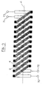
- a plurality of first wirings 2 each having a rectangular shape which is, for example, 2 ⁇ m wide and 50 ⁇ m long, are arranged along a desired virtual line 6 on a semi-insulating semiconductor substrate 1 so that the first wirings 2 intersect the virtual line 6.
- a metal such as Ti/Au or the like is used for the first-layer wirings 2 and the thickness thereof is 0.5 ⁇ m - 1 ⁇ m.
- an inter-layer insulating film 3 ordinarily having a thickness of several thousands angstroms is formed of Si3N4, SiON or the like. Thereafter, through-holes are formed by etching by removing portions corresponding to contact holes 5 from the inter-layer insulating film 3.
- a photoresist is applied to be as thick as possible, provided that exposure and development can occur. If the type of photoresist and condition for applying the photoresist are suitably selected, the photoresist can be applied to a thickness of about 20 ⁇ m.
- the photoresist is then removed at the portions corresponding to the contact holes 5 by exposure and development, so that second-layer wirings 4, which will be formed later, can be electrically connected to the first-layer wirings 2.
- the shape at the upper end portions of the photoresist is made round by baking at a temperature of about 140°C. The baking is to make the throwing power good in forming the conductors of the second-layer wirings 4.
- the second-layer wirings 4 is formed by evaporating deposition or sputtering and then Au is deposited thereon by plating, thereby forming the second-layer wirings 4.
- the thickness of the second-layer wirings 4 is ordinarily selected to be 2 ⁇ m - 3 ⁇ m.
- the photoresist is removed so that a hollow air bridge 13 is formed between the first-layer wirings 2 and the second-layer wirings 4.
- the inter-layer insulating film 3 is left as is on the first-layer wirings 2.
- an inductor element 10 is formed having a spiral structure constituted by the first-layer wirings 2, the second-layer wirings 4 and the contact holes 5.
- Such an inductor element 10 may be formed even without application of the air bridge technique in the final step.
- the inter-layer insulating film 3 may be formed to be thicker and then the second-layer wirings 4 may be formed directly thereon.
- the use of the air bridge technique is, however, advantageous for the following reasons. Because the inductance value increases as the sectional area S1 increases, the area occupied by the inductor element as required for obtaining the same inductance value, becomes smaller, which is apparent from expression (1). Accordingly, size reduction of the MMIC can be achieved by using the air bridge structure to increase the sectional area S1.
- the distributed capacity becomes smaller not only by increasing the distance between the first-layer wirings 2 and the second-layer wirings 4, but by removing the photoresist as an insulating substance. Accordingly, the self resonance frequency, i.e., the maximum limit frequency allowing this element to use as an inductor element, becomes larger.
- the width w of the windings is smaller because the occupied area decreases as the width w decreases, the resistance of the wirings becomes larger and, accordingly, Q of the inductance becomes smaller. Accordingly, the width must be determined on the basis of the value of Q allowable in accordance with the frequency, inductance or the like to be used, and the resistance of the wirings. It is now assumed that the width is 10 ⁇ m. Although it is advantageous to select the height h of the air bridge to be larger, it is apparent from the point of view of supporting strength that the length d of the air bridge in the horizontal direction must be reduced as the height h increases.
- the height h is determined to an optimum value taking the sectional area and the occupied area into consideration. It is now assumed that the height h of the air bridge and the length d of the same are 20 ⁇ m and 120 ⁇ m, respectively. These are values which can be obtained in practical use.
- the pitch p between adjacent wirings can approach about 12 ⁇ m. If the pitch is made to sufficiently approach the above-mentioned value, the distributed capacity becomes larger and, accordingly, the self resonance frequency becomes smaller. Accordingly, the pitch p between adjacent wirings is determined on the basis of the self resonance frequency which is allowed.
- the inductance value can be calculated proportionally to the number of turns according to the aforementioned expression (1).
- the number of turns is 40 though only five turns are shown in the drawings for the simplification of description, the inductance value is calculated as follows.
- the sectional is assumed to be a rectangle and the thickness of the inter-layer insulating film is neglected.
- the inductance value becomes 4.8nH when a plane-type spiral inductor is formed with an area of 300 ⁇ m ⁇ 300 ⁇ m.
- the inductance value is 6.71nH when the inductor is formed with an occupied area of 600 ⁇ m ⁇ 120 ⁇ m. Accordingly, the inductance per unit area of the flat-type spiral inductor is 0.053pH/ ⁇ m2 whereas the inductance per unit area of the inductor according to the invention is 0.093pH/ ⁇ m2, which is 1.75 times greater. Further, the inductor according to the invention has a long and narrow structure, so that the longitudinal direction (the direction of the virtual line 6 can be bent if necessary. Accordingly, the inductor of the transformer of the invention has an advantage in that the degree of freedom on layout design is too large to form a dead space in the MMIC, compared with the conventional spiral inductor.
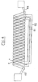
- the inductor element 10 thus produced is three-dimensional so that it can be dealt with in the same manner as an ordinary coil. Accordingly, when terminals 7, 8 and 9 extend from the opposite ends of the inductor element and a predetermined intermediate point thereof, a transformer 12 is provided using the terminals 7 and 9 as primary electrodes and the terminals 8 and 9 as secondary electrodes.
- a second embodiment of the present invention is shown in Figs. 4 through 6.
- the second embodiment is different from the first embodiment in that a belt-like magnetic substance 20 is provided in the spiral structure.
- the first-layer wirings 2 and the inter-layer insulating film 3 are formed in the same manner as in the first embodiment. Then, a magnetic material such as Fe, Ni, Co, ferrite or the like is deposited on the inter-layer insulating film 3 by sputtering or the like and then a magnetic core 20 is formed so as to have a belt-like shape. The steps thereafter is substantially the same as in the first embodiment.
- the expression (3) is used to calculate the inductance value of the inductor element.
- the inductance L is calculated as follows. Because K is larger than 1, a larger value can be obtained compared with the first embodiment having no magnetic substance (magnetic core) 20. In other words, this embodiment provides a size advantage.
- Fig. 7 shows a further embodiment in which the opposite ends of each of the second-layer wirings 4 are connected to the first-layer wirings 2 at intervals of one first-layer wiring. Accordingly, two combinations of inductor elements are formed coaxially so as to overlap each other coaxially. As a result, a transformer can be formed by using the opposite ends (terminals 70 and 71) of one inductor element as primary electrodes and the opposite ends (terminals 72 and 73) of the other inductor element as secondary electrodes. When the number of first-layer wirings 2 skipped by each of the second-layer wirings 4 is increased in the same manner as described above, three or more combinations of inductor elements can be formed so as to overlap each other coaxially.
- the transformer according to the invention is a transmission-line transformer which theoretically has a wide frequency band. Accordingly, when triple-spiral structure inductor elements are connected by wirings 81 to 84 as shown in Fig. 8, it is possible to provide a 1:9 impedance transformer.
- a passive transformer which has previously not been provided in the conventional MMIC can be formed as an integrated circuit.
- the transformer includes an inductor element having a long and narrow structure so that it can be bent suitably on the substrate. Accordingly, the inductor element improves the degree of freedom on layout design, as compared with the conventional plane-type spiral inductor.
Abstract
A passive transformer which can be formed in an MMIC having a plurality of first-layer wirings formed on a substrate so that each of the first-layer wirings intersects a desired virtual line on the substrate; an insulating film for covering a substrate surface on which the first-layer wirings are formed; and a plurality of second-layer wirings formed on the insulating film so that each of the second-layer wirings intersects the virtual line and has opposite ends respectively connected to different ends of the first-layer wirings through contact holes. An inductor element having a spiral structure along the virtual line constitutes the first-layer wirings the contact holes and the second-layer wirings. The opposite ends of the inductor element are primary electrodes, and one end and a desired intermediate point of the inductor element are secondary electrodes. Because the transformer has such a structure, a three-dimensional coil can be formed on the substrate so that the transformer can be formed in an MMIC.
Description
- The present invention relates to a transformer for performing impedance transformation or for performing separation of a ground circuit in a microwave integrated circuit. The transformer includes an inductor element formed on a substrate which is used for blocking (shunting) or passing a high frequency signal or for constituting a filter in combination with a capacitance element and/or a resistor element, for processing a high-frequency signal of from several hundreds MHz to several tens GHz.
- With rapid advances in the development of information network systems, satellite communication system in a high frequency band are becoming more popular. As a result, a high-frequency field-effect transistor, a Schottky barrier type field-effect transistor (MESFET) using a compound semiconductor such as a GaAs semiconductor or the like is being used more and more. Recently, in order to reduce the size and cost of the system for such communication and in order to improve system performance, a first-stage amplifier portion of a down converter for converting a high-frequency signal into a low-frequency signal has been developed and fabricated into an integrated circuit (MMIC: monolithic microwave integrated circuit). The MMIC provides a communication device replacing one constituted by a large number of separate elements. The use of such an MMIC reduces the number of parts, the mounting costs and improves reliability by reducing the number of connection points required by the circuit. Compared with prior devices using a large number of separate elements, reduction in cost can be easily achieved.
- Although it is required that a transformer for performing impedance transformation or performing separation of a ground circuit be provided in the form of a MMIC, in a conventional MMIC, an active element has been used to perform the transformer function. The use of these active elements such as an inductor element using a distributed constant line element and a spiral inductor, however, create problems. For example, when using the distributed constant line element such as a micro strip line, there is a tendency for the area of the strip line to become large. This tendency becomes significant in a MMIC for use at low frequencies. As the size of the MMIC chip becomes large, production yield becomes low and the number of chips which can be obtained from a semiconductor substrate becomes relatively smaller, thus, increasing the cost per chip. In the case of a spiral inductor constituted by spirally shaping a line with a width of about 2µm - about 20µm, it becomes impossible to form a transformer in view of the inductor structure. Accordingly, a transformer cannot be effectively achieved by using an active element.
- The pseudo transformer using an active element reduces the size of the MMIC but increases electric power consumption. Therefore, it is not always desirable to use an active element.
- It is an object of the present invention to provide a passive transformer which can be used in a conventional MMIC and which overcomes the problems stated above. In accordance with the principles of the present invention a transformer provided with a plurality of first-layer wirings formed on a substrate so that each of the first-layer wirings intersects a desired virtual line on the substrate; an insulating film for covering a substrate surface on which the first-layer wirings are formed; and a plurality of second-layer wirings formed on the insulating film so that each of the second-layer wirings intersects the virtual line and has opposite ends respectively connected to different ends of the first-layer wirings through contact holes. An inductor element having a spiral structure along the virtual line is constituted by the first-layer wirings, the contact holes and the second-layer wirings. Opposite ends of the inductor element are made to be primary electrodes, and one end and a desired intermediate point of the inductor element are made to be secondary electrodes. Further, each of the second-layer wirings has one end connected to one of the first-layer wirings and the other end connected to the n-th (n being a natural number not smaller than 2) order first-layer wiring counted from the one first-layer wiring, whereby n combinations of inductor elements are constituted along one and the same virtual line by the first-layer wirings, the contact holes and the second-layer wirings. The opposite ends of one of the inductor elements are made to be primary electrodes and the opposite ends of other inductor elements are made to be secondary electrodes.
- It is a further object of the invention to provide an inductor element for use in an MMIC which reduces the size of the MMIC, and which is easy to manufacture.
- In accordance with the present invention, a three-dimensional inductor element is constituted on a substrate by first-layer wirings, second-layer wirings and contact holes connecting the first-and second-layer wirings. The inductance value of the inductor element according to the present invention can be calculated in the same manner as an ordinary solenoid. That is, the self inductance L₁ of a sufficient long solenoid having a sectional area S₁, a length (length along the virtual line) l₁ and the number of turns n₁ per unit length can be calculated as follows.

- Although this equation is an expression for calculating the self inductance of a solenoid of an air-core (with a specific permeability of µ₀), the self inductance of a solenoid having a specific permeability µ can be calculated as follows.

- Because the inside of the solenoid according to the present invention cannot be perfectly filled with the magnetic substance, the self inductance thereof can be calculated as follows.

where 1<K<µ
Since a three-dimensional inductor element (coil) is formed on a semiconductor substrate, a transformer can be formed in the same manner as a transformer formed as a separate part. -
- Fig. 1 is a sectional view of a transformer as an embodiment of the present invention;
- Fig. 2 is a plan view of a transformer as an embodiment of the present invention;
- Fig. 3 is a perspective of a transformer as an embodiment of the present invention;
- Fig. 4 is a sectional view of a transformer as a second embodiment of the present invention.
- Fig. 5 is a plan view of a transformer as a second embodiment of the present invention;
- Fig. 6 is a perspective view of a transformer as a second embodiment of the present invention;
- Fig. 7 is a schematic plan view of a transformer as a third embodiment of the present invention;
- Fig. 8 is a schematic plan view of a transformer wired to form an impedance transformer as a fourth embodiment of the present invention;
- As shown in Figs. 1-3, a plurality of
first wirings 2 each having a rectangular shape which is, for example, 2µm wide and 50µm long, are arranged along a desiredvirtual line 6 on asemi-insulating semiconductor substrate 1 so that thefirst wirings 2 intersect thevirtual line 6. A metal such as Ti/Au or the like is used for the first-layer wirings 2 and the thickness thereof is 0.5µm - 1µm. - Then, an inter-layer insulating
film 3 ordinarily having a thickness of several thousands angstroms is formed of Si₃N₄, SiON or the like. Thereafter, through-holes are formed by etching by removing portions corresponding tocontact holes 5 from the inter-layer insulatingfilm 3. - Next, a photoresist is applied to be as thick as possible, provided that exposure and development can occur. If the type of photoresist and condition for applying the photoresist are suitably selected, the photoresist can be applied to a thickness of about 20µm. The photoresist is then removed at the portions corresponding to the
contact holes 5 by exposure and development, so that second-layer wirings 4, which will be formed later, can be electrically connected to the first-layer wirings 2. After the completion of the patterning, the shape at the upper end portions of the photoresist is made round by baking at a temperature of about 140°C. The baking is to make the throwing power good in forming the conductors of the second-layer wirings 4. Next, a metal such as Ti/Au or the like is formed by evaporating deposition or sputtering and then Au is deposited thereon by plating, thereby forming the second-layer wirings 4. The thickness of the second-layer wirings 4 is ordinarily selected to be 2µm - 3µm. - After the second-
layer wirings 4 have been formed as described above, the photoresist is removed so that ahollow air bridge 13 is formed between the first-layer wirings 2 and the second-layer wirings 4. However, the inter-layerinsulating film 3 is left as is on the first-layer wirings 2. - Through the aforementioned steps, an
inductor element 10 is formed having a spiral structure constituted by the first-layer wirings 2, the second-layer wirings 4 and thecontact holes 5. - Such an
inductor element 10 may be formed even without application of the air bridge technique in the final step. For example, the inter-layerinsulating film 3 may be formed to be thicker and then the second-layer wirings 4 may be formed directly thereon. The use of the air bridge technique is, however, advantageous for the following reasons. Because the inductance value increases as the sectional area S₁ increases, the area occupied by the inductor element as required for obtaining the same inductance value, becomes smaller, which is apparent from expression (1). Accordingly, size reduction of the MMIC can be achieved by using the air bridge structure to increase the sectional area S₁. Further, the distributed capacity becomes smaller not only by increasing the distance between the first-layer wirings 2 and the second-layer wirings 4, but by removing the photoresist as an insulating substance. Accordingly, the self resonance frequency, i.e., the maximum limit frequency allowing this element to use as an inductor element, becomes larger. - An example of calculation of the inductance value of the
inductor element 10 in this embodiment will be described hereunder. Although it is advantageous to select the width w of the windings to be smaller because the occupied area decreases as the width w decreases, the resistance of the wirings becomes larger and, accordingly, Q of the inductance becomes smaller. Accordingly, the width must be determined on the basis of the value of Q allowable in accordance with the frequency, inductance or the like to be used, and the resistance of the wirings. It is now assumed that the width is 10µm. Although it is advantageous to select the height h of the air bridge to be larger, it is apparent from the point of view of supporting strength that the length d of the air bridge in the horizontal direction must be reduced as the height h increases. Therefore, the height h is determined to an optimum value taking the sectional area and the occupied area into consideration. It is now assumed that the height h of the air bridge and the length d of the same are 20µm and 120µm, respectively. These are values which can be obtained in practical use. In the case where the width w of the wirings is 10µm, the pitch p between adjacent wirings can approach about 12µm. If the pitch is made to sufficiently approach the above-mentioned value, the distributed capacity becomes larger and, accordingly, the self resonance frequency becomes smaller. Accordingly, the pitch p between adjacent wirings is determined on the basis of the self resonance frequency which is allowed. - Next, it is assumed that the pitch p is 15µm. Here, the inductance value can be calculated proportionally to the number of turns according to the aforementioned expression (1). When, for example, the number of turns is 40 though only five turns are shown in the drawings for the simplification of description, the inductance value is calculated as follows.

- In the aforementioned expressions, the sectional is assumed to be a rectangle and the thickness of the inter-layer insulating film is neglected.
- According to the Autumn National Meeting C-56, 1990, of the Institute of Electronics, Information and Communication Engineers of Japan, the inductance value becomes 4.8nH when a plane-type spiral inductor is formed with an area of 300µm×300µm.
- In the aforementioned example of calculation, the inductance value is 6.71nH when the inductor is formed with an occupied area of 600µm×120µm. Accordingly, the inductance per unit area of the flat-type spiral inductor is 0.053pH/µm² whereas the inductance per unit area of the inductor according to the invention is 0.093pH/µm², which is 1.75 times greater. Further, the inductor according to the invention has a long and narrow structure, so that the longitudinal direction (the direction of the
virtual line 6 can be bent if necessary. Accordingly, the inductor of the transformer of the invention has an advantage in that the degree of freedom on layout design is too large to form a dead space in the MMIC, compared with the conventional spiral inductor. - The
inductor element 10 thus produced is three-dimensional so that it can be dealt with in the same manner as an ordinary coil. Accordingly, whenterminals 7, 8 and 9 extend from the opposite ends of the inductor element and a predetermined intermediate point thereof, atransformer 12 is provided using theterminals 7 and 9 as primary electrodes and the terminals 8 and 9 as secondary electrodes. - A second embodiment of the present invention is shown in Figs. 4 through 6. The second embodiment is different from the first embodiment in that a belt-like
magnetic substance 20 is provided in the spiral structure. - The first-
layer wirings 2 and the inter-layerinsulating film 3 are formed in the same manner as in the first embodiment. Then, a magnetic material such as Fe, Ni, Co, ferrite or the like is deposited on the inter-layerinsulating film 3 by sputtering or the like and then amagnetic core 20 is formed so as to have a belt-like shape. The steps thereafter is substantially the same as in the first embodiment. - In the second embodiment, the expression (3) is used to calculate the inductance value of the inductor element. When the width w of the windings, the height h of the air bridge, the horizontal length d of the air bridge, the pitch p between adjacent wirings and the number of turns are respectively equal to those in the first embodiment, the inductance L, is calculated as follows.

Because K is larger than 1, a larger value can be obtained compared with the first embodiment having no magnetic substance (magnetic core) 20. In other words, this embodiment provides a size advantage. - Fig. 7 shows a further embodiment in which the opposite ends of each of the second-
layer wirings 4 are connected to the first-layer wirings 2 at intervals of one first-layer wiring. Accordingly, two combinations of inductor elements are formed coaxially so as to overlap each other coaxially. As a result, a transformer can be formed by using the opposite ends (terminals 70 and 71) of one inductor element as primary electrodes and the opposite ends (terminals 72 and 73) of the other inductor element as secondary electrodes. When the number of first-layer wirings 2 skipped by each of the second-layer wirings 4 is increased in the same manner as described above, three or more combinations of inductor elements can be formed so as to overlap each other coaxially. - The transformer according to the invention is a transmission-line transformer which theoretically has a wide frequency band. Accordingly, when triple-spiral structure inductor elements are connected by wirings 81 to 84 as shown in Fig. 8, it is possible to provide a 1:9 impedance transformer.
- As described above, according to the present invention, a passive transformer which has previously not been provided in the conventional MMIC can be formed as an integrated circuit. The transformer includes an inductor element having a long and narrow structure so that it can be bent suitably on the substrate. Accordingly, the inductor element improves the degree of freedom on layout design, as compared with the conventional plane-type spiral inductor.
- While the present invention has been described in connection with what is presently considered to be the most practical and preferred embodiments, it is understood that the invention is not limited to the disclosed embodiments, but, on the contrary, is intended to cover various modifications and equivalent arrangements included within the spirit and scope of the appended claims.
Claims (15)
- A transformer comprising:
a plurality of first-layer wirings formed on a substrate so that each of said first-layer wirings intersects a desired virtual line on said substrate;
an insulating film for covering a substrate surface on which said first-layer wirings are formed; and
a plurality of second-layer wirings formed on said insulating film so that each of said second-layer wirings intersects said virtual line and has opposite ends respectively connected to different ends of said first-layer wirings through contact holes; wherein
an inductor element having a spiral structure along said virtual line being formed by said first-layer wirings, said contact holes and said second-layer wirings, opposite ends of said inductor element being primary electrodes, and one of said opposite ends and a desired intermediate point of said inductor element being secondary electrodes. - A transformer according to claim 1, wherein said second-layer wirings have an air bridge structure.
- A transformer according to claim 1, wherein a magnetic substance is provided between said insulating film and said second-layer wirings disposed along said virtual line.
- A transformer according to claim 1, wherein the thickness of said first-layer is at least 0.5µm but not more than 1µm and the thickness of said second-layer is between 2µm - 3µm.
- A transformer according to claim 1, wherein said first-layer and said second-layer are each composed of Ti/Au.
- A transformer comprising:
a plurality of first-layer wirings formed on a substrate so that each of said first-layer wirings intersects a desired virtual line on said substrate;
an insulating film for covering a substrate surface on which said first-layer wirings are formed; and
a plurality of second-layer wirings formed on said insulating film so that each of said second-layer wirings intersects said virtual line and has opposite ends respectively connected to different ends of said first-layer wirings through contact holes;
said second-layer wirings having one end connected to one of said first-layer wirings and the other end connected to the n-th (n being a natural number not smaller than 2) order first-layer wiring counted from said one first-layer wiring, whereby n combinations of inductor elements are constituted along one and the same virtual line by said first-layer wirings, said contact holes and said second-layer wirings,
opposite ends of one inductor element being primary electrodes and the opposite ends of another inductor element being secondary electrodes. - A transformer according to claim 6, wherein said second-layer wirings have an air bridge structure.
- A transformer according to claim 6, wherein a magnetic substance is provided between said insulating film and said second-layer wirings so as to be disposed along said virtual line.
- An inductor element comprising:
a plurality of first-layer wirings formed on a substrate so that each of said first-layer wirings intersects a desired virtual line on said substrate;
an insulating film for covering a substrate surface on which said first-layer wirings are formed; and
a plurality of second-layer wirings formed on said insulating film so that each of said second-layer wirings intersects said virtual line and has opposite ends respectively connected to different ends of said first-layer wirings through contact holes;
whereby a spiral structure along said virtual line is constituted by said first-layer wirings, said contact holes and said second-layer wirings. - An inductor element according to claim 9, wherein said second-layer wirings have an air bridge structure.
- An inductor element according to claim 9, wherein a magnetic substance is provided between said insulating film and said second-layer wirings disposed along said virtual line.
- An inductor element according to claim 9, wherein the thickness of the first-layer is at least 0.5µm but not more than 1µm and the thickness of said second-layer is between 2µm - 3µm.
- An inductor element according to claim 9, wherein said first-layer and said second-layer are each composed of Ti/Au.
- A method of manufacturing a transformer comprising the steps of:
arranging a plurality of first wirings along a desired virtual line on a semiconductor substrate so that said first wirings intersect with said virtual line;
forming an inter-layer insulating film which covers a substrate surface on which said first wirings are formed;
forming holes through said insulating film which correspond to contact points;
applying a photoresist at least over said holes;
removing the photoresist by exposure and development at points corresponding to the contact points;
forming a plurality of second-layer wiring on said insulating film so that each of said second layer wirings intersects said virtual line and has opposite ends respectively connected to different ends of said first-layer wirings at said contact points; and
forming primary and secondary electrodes at predetermined points. - A method of manufacturing an inductor comprising the steps of:
arranging a plurality of first wirings along a desired virtual line on a semiconductor substrate so that said first wirings intersect with said virtual line;
forming an inter-layer insulating film which covers a substrate surface on which said first wirings are formed;
forming holes through said insulating film which correspond to contact points;
applying a photoresist over said holes;
removing the photoresist by exposure and development at points corresponding to the contact points; and
forming a plurality of second-layer wiring on said insulating film so that each of said second layer wirings intersects said virtual line and has opposite ends respectively connected to different ends of said first-layer wirings at said contact points.
Applications Claiming Priority (4)
| Application Number | Priority Date | Filing Date | Title |
|---|---|---|---|
| JP12966991A JPH04354108A (en) | 1991-05-31 | 1991-05-31 | Inductor element |
| JP129673/91 | 1991-05-31 | ||
| JP12967391A JPH04354308A (en) | 1991-05-31 | 1991-05-31 | Transformer |
| JP129669/91 | 1991-05-31 |
Publications (1)
| Publication Number | Publication Date |
|---|---|
| EP0515821A1 true EP0515821A1 (en) | 1992-12-02 |
Family
ID=26464987
Family Applications (1)
| Application Number | Title | Priority Date | Filing Date |
|---|---|---|---|
| EP92106534A Withdrawn EP0515821A1 (en) | 1991-05-31 | 1992-04-15 | Inductor element and transformer for monolithic microwave integrated circuit |
Country Status (3)
| Country | Link |
|---|---|
| US (1) | US5425167A (en) |
| EP (1) | EP0515821A1 (en) |
| CA (1) | CA2062710C (en) |
Cited By (6)
| Publication number | Priority date | Publication date | Assignee | Title |
|---|---|---|---|---|
| EP0654802A1 (en) * | 1993-11-17 | 1995-05-24 | Takeshi Ikeda | Variable inductance element |
| EP0942441A2 (en) * | 1998-03-10 | 1999-09-15 | Smart Card Technologies Co., Ltd. | Coil element and method for manufacturing thereof |
| WO2000010179A1 (en) * | 1998-08-14 | 2000-02-24 | Samsung Electronics Co., Ltd. | Bonding wire inductor and manufacturing method thereof |
| US6803665B1 (en) * | 2001-11-02 | 2004-10-12 | Skyworks Solutions, Inc. | Off-chip inductor |
| KR100469248B1 (en) * | 2001-12-24 | 2005-02-02 | 엘지전자 주식회사 | MicroInductor for Wireless Communication Module |
| WO2011025423A1 (en) * | 2009-08-27 | 2011-03-03 | Telefonaktiebolaget L M Ericsson (Publ) | An improved transformer |
Families Citing this family (27)
| Publication number | Priority date | Publication date | Assignee | Title |
|---|---|---|---|---|
| US5939966A (en) * | 1994-06-02 | 1999-08-17 | Ricoh Company, Ltd. | Inductor, transformer, and manufacturing method thereof |
| US5781091A (en) * | 1995-07-24 | 1998-07-14 | Autosplice Systems Inc. | Electronic inductive device and method for manufacturing |
| KR100211814B1 (en) * | 1995-11-30 | 1999-08-02 | 전주범 | A pliability coil winding structure of fbt and manufacture method therefore |
| US5793272A (en) * | 1996-08-23 | 1998-08-11 | International Business Machines Corporation | Integrated circuit toroidal inductor |
| US6249039B1 (en) | 1998-09-10 | 2001-06-19 | Bourns, Inc. | Integrated inductive components and method of fabricating such components |
| US6147582A (en) * | 1999-03-04 | 2000-11-14 | Raytheon Company | Substrate supported three-dimensional micro-coil |
| US6292086B1 (en) * | 1999-10-12 | 2001-09-18 | Agere Systems Guardian Corp. | Lateral high-Q inductor for semiconductor devices |
| US6396677B1 (en) | 2000-05-17 | 2002-05-28 | Xerox Corporation | Photolithographically-patterned variable capacitor structures and method of making |
| US6856225B1 (en) * | 2000-05-17 | 2005-02-15 | Xerox Corporation | Photolithographically-patterned out-of-plane coil structures and method of making |
| US6392524B1 (en) | 2000-06-09 | 2002-05-21 | Xerox Corporation | Photolithographically-patterned out-of-plane coil structures and method of making |
| FR2811135B1 (en) * | 2000-06-29 | 2002-11-22 | Memscap | MICRO-COMPONENT OF THE MICRO-INDUCTANCE OR MICRO-TRANSFORMER TYPE |
| US6595787B2 (en) * | 2001-02-09 | 2003-07-22 | Xerox Corporation | Low cost integrated out-of-plane micro-device structures and method of making |
| KR100368930B1 (en) * | 2001-03-29 | 2003-01-24 | 한국과학기술원 | Three-Dimensional Metal Devices Highly Suspended above Semiconductor Substrate, Their Circuit Model, and Method for Manufacturing the Same |
| EP1407545A1 (en) * | 2001-07-04 | 2004-04-14 | Koninklijke Philips Electronics N.V. | Electronic inductive and capacitive component |
| JP3983199B2 (en) * | 2003-05-26 | 2007-09-26 | 沖電気工業株式会社 | Semiconductor device and manufacturing method thereof |
| US20050093667A1 (en) * | 2003-11-03 | 2005-05-05 | Arnd Kilian | Three-dimensional inductive micro components |
| US6998952B2 (en) * | 2003-12-05 | 2006-02-14 | Freescale Semiconductor, Inc. | Inductive device including bond wires |
| US7570129B2 (en) * | 2005-09-02 | 2009-08-04 | Northrop Grumman Corporation | 3D MMIC balun and methods of making the same |
| US7524731B2 (en) * | 2006-09-29 | 2009-04-28 | Freescale Semiconductor, Inc. | Process of forming an electronic device including an inductor |
| US7724484B2 (en) * | 2006-12-29 | 2010-05-25 | Cobham Defense Electronic Systems Corporation | Ultra broadband 10-W CW integrated limiter |
| TWI345243B (en) * | 2007-08-14 | 2011-07-11 | Ind Tech Res Inst | Inter-helix inductor devices |
| TWI345417B (en) * | 2007-09-07 | 2011-07-11 | Himax Tech Ltd | Tuner and transformer formed by printed circuit board thereof |
| US9721715B2 (en) * | 2009-01-22 | 2017-08-01 | 2Sentient Inc. | Solid state components having an air core |
| US20100259349A1 (en) * | 2009-04-09 | 2010-10-14 | Qualcomm Incorporated | Magnetic Film Enhanced Inductor |
| JP5603788B2 (en) * | 2011-01-21 | 2014-10-08 | アンリツ株式会社 | Coil and manufacturing method thereof |
| US20130119511A1 (en) * | 2011-11-10 | 2013-05-16 | Taiwan Semiconductor Manufacturing Company, Ltd. | Inductor having bond-wire and manufacturing method thereof |
| US20140203902A1 (en) * | 2013-01-18 | 2014-07-24 | Geoffrey D. Shippee | Cards, devices, electromagnetic field generators and methods of manufacturing electromagnetic field generators |
Citations (6)
| Publication number | Priority date | Publication date | Assignee | Title |
|---|---|---|---|---|
| US3992691A (en) * | 1975-07-02 | 1976-11-16 | Cubic Corporation | Electronic circuit board flat coil inductor |
| DE3418379A1 (en) * | 1983-05-18 | 1984-11-22 | Murata Manufacturing Co., Ltd., Nagaokakyo, Kyoto | LAYERED INDUCTION COIL |
| DE3423139A1 (en) * | 1983-06-23 | 1985-01-10 | Murata Eria N.A., Inc., Marietta, Ga. | Monolithic inductor having transformer applications |
| DE3346659A1 (en) * | 1983-12-23 | 1985-07-04 | Standard Elektrik Lorenz Ag, 7000 Stuttgart | Inductive component |
| DE3441218A1 (en) * | 1984-11-10 | 1986-05-15 | Wilde Membran Impuls Technik GmbH, 5828 Ennepetal | Induction-coil arrangement for electrical circuits |
| DE3927181A1 (en) * | 1988-08-19 | 1990-03-01 | Murata Manufacturing Co | COIL CHIP AND MANUFACTURING METHOD THEREFOR |
Family Cites Families (3)
| Publication number | Priority date | Publication date | Assignee | Title |
|---|---|---|---|---|
| US3290758A (en) * | 1963-08-07 | 1966-12-13 | Hybrid solid state device | |
| US3561110A (en) * | 1967-08-31 | 1971-02-09 | Ibm | Method of making connections and conductive paths |
| BE862654A (en) * | 1977-01-13 | 1978-07-05 | Cit Alcatel | INDUCTIVE CIRCUITS REALIZATION PROCESS |
-
1992
- 1992-03-11 CA CA002062710A patent/CA2062710C/en not_active Expired - Fee Related
- 1992-04-15 EP EP92106534A patent/EP0515821A1/en not_active Withdrawn
-
1994
- 1994-08-29 US US08/297,518 patent/US5425167A/en not_active Expired - Fee Related
Patent Citations (6)
| Publication number | Priority date | Publication date | Assignee | Title |
|---|---|---|---|---|
| US3992691A (en) * | 1975-07-02 | 1976-11-16 | Cubic Corporation | Electronic circuit board flat coil inductor |
| DE3418379A1 (en) * | 1983-05-18 | 1984-11-22 | Murata Manufacturing Co., Ltd., Nagaokakyo, Kyoto | LAYERED INDUCTION COIL |
| DE3423139A1 (en) * | 1983-06-23 | 1985-01-10 | Murata Eria N.A., Inc., Marietta, Ga. | Monolithic inductor having transformer applications |
| DE3346659A1 (en) * | 1983-12-23 | 1985-07-04 | Standard Elektrik Lorenz Ag, 7000 Stuttgart | Inductive component |
| DE3441218A1 (en) * | 1984-11-10 | 1986-05-15 | Wilde Membran Impuls Technik GmbH, 5828 Ennepetal | Induction-coil arrangement for electrical circuits |
| DE3927181A1 (en) * | 1988-08-19 | 1990-03-01 | Murata Manufacturing Co | COIL CHIP AND MANUFACTURING METHOD THEREFOR |
Cited By (10)
| Publication number | Priority date | Publication date | Assignee | Title |
|---|---|---|---|---|
| EP0654802A1 (en) * | 1993-11-17 | 1995-05-24 | Takeshi Ikeda | Variable inductance element |
| US5629553A (en) * | 1993-11-17 | 1997-05-13 | Takeshi Ikeda | Variable inductance element using an inductor conductor |
| EP0942441A2 (en) * | 1998-03-10 | 1999-09-15 | Smart Card Technologies Co., Ltd. | Coil element and method for manufacturing thereof |
| EP0942441A3 (en) * | 1998-03-10 | 1999-12-08 | Smart Card Technologies Co., Ltd. | Coil element and method for manufacturing thereof |
| US6367143B1 (en) | 1998-03-10 | 2002-04-09 | Smart Card Technologies Co. Ltd. | Coil element and method for manufacturing thereof |
| WO2000010179A1 (en) * | 1998-08-14 | 2000-02-24 | Samsung Electronics Co., Ltd. | Bonding wire inductor and manufacturing method thereof |
| US6775901B1 (en) | 1998-08-14 | 2004-08-17 | Hai Young Lee | Bonding wire inductor |
| US6803665B1 (en) * | 2001-11-02 | 2004-10-12 | Skyworks Solutions, Inc. | Off-chip inductor |
| KR100469248B1 (en) * | 2001-12-24 | 2005-02-02 | 엘지전자 주식회사 | MicroInductor for Wireless Communication Module |
| WO2011025423A1 (en) * | 2009-08-27 | 2011-03-03 | Telefonaktiebolaget L M Ericsson (Publ) | An improved transformer |
Also Published As
| Publication number | Publication date |
|---|---|
| US5425167A (en) | 1995-06-20 |
| CA2062710A1 (en) | 1992-12-01 |
| CA2062710C (en) | 1996-05-14 |
Similar Documents
| Publication | Publication Date | Title |
|---|---|---|
| EP0515821A1 (en) | Inductor element and transformer for monolithic microwave integrated circuit | |
| US3614554A (en) | Miniaturized thin film inductors for use in integrated circuits | |
| EP0778593B1 (en) | Method for realizing magnetic circuits in an integrated circuit | |
| US8518789B2 (en) | Integrated electronic device and method of making the same | |
| JP3141562B2 (en) | Thin film transformer device | |
| US7678639B2 (en) | Inductor formed in an integrated circuit | |
| US5279988A (en) | Process for making microcomponents integrated circuits | |
| EP0643403B1 (en) | Inductive structures for semiconductor integrated circuits | |
| EP0523450A1 (en) | Inductance element | |
| US6621141B1 (en) | Out-of-plane microcoil with ground-plane structure | |
| JPH0319358A (en) | Semiconductor integrated circuit | |
| EP0515824A2 (en) | Capacitor element | |
| EP1248297A2 (en) | Inductance element and semiconductor device | |
| EP0436385A2 (en) | High-frequency inductor and manufacturing method thereof | |
| KR100469248B1 (en) | MicroInductor for Wireless Communication Module | |
| EP0750364A2 (en) | Chip antenna | |
| JPH08172161A (en) | Inductor element and its manufacture and monolithic microwave integrated circuit using the same | |
| US6781229B1 (en) | Method for integrating passives on-die utilizing under bump metal and related structure | |
| JPH10154795A (en) | Inductor on semiconductor chip and its manufacturing method | |
| JPH10290105A (en) | High frequency wiring board | |
| JPH04354108A (en) | Inductor element | |
| JPH06151718A (en) | Inductor element in semiconductor device | |
| JPH04354308A (en) | Transformer | |
| JPH10270248A (en) | Spiral inductor | |
| JPH0513235A (en) | Inductance element |
Legal Events
| Date | Code | Title | Description |
|---|---|---|---|
| PUAI | Public reference made under article 153(3) epc to a published international application that has entered the european phase |
Free format text: ORIGINAL CODE: 0009012 |
|
| AK | Designated contracting states |
Kind code of ref document: A1 Designated state(s): DE FR GB NL SE |
|
| 17P | Request for examination filed |
Effective date: 19930219 |
|
| 17Q | First examination report despatched |
Effective date: 19950123 |
|
| GRAH | Despatch of communication of intention to grant a patent |
Free format text: ORIGINAL CODE: EPIDOS IGRA |
|
| STAA | Information on the status of an ep patent application or granted ep patent |
Free format text: STATUS: THE APPLICATION IS DEEMED TO BE WITHDRAWN |
|
| 18D | Application deemed to be withdrawn |
Effective date: 19960509 |