EP0510976B1 - Level independent automatic cable equalizer - Google Patents
Level independent automatic cable equalizer Download PDFInfo
- Publication number
- EP0510976B1 EP0510976B1 EP92303664A EP92303664A EP0510976B1 EP 0510976 B1 EP0510976 B1 EP 0510976B1 EP 92303664 A EP92303664 A EP 92303664A EP 92303664 A EP92303664 A EP 92303664A EP 0510976 B1 EP0510976 B1 EP 0510976B1
- Authority
- EP
- European Patent Office
- Prior art keywords
- input
- output
- signal
- coupled
- equalizer
- Prior art date
- Legal status (The legal status is an assumption and is not a legal conclusion. Google has not performed a legal analysis and makes no representation as to the accuracy of the status listed.)
- Expired - Lifetime
Links
Images


Classifications
-
- H—ELECTRICITY
- H03—ELECTRONIC CIRCUITRY
- H03G—CONTROL OF AMPLIFICATION
- H03G3/00—Gain control in amplifiers or frequency changers without distortion of the input signal
- H03G3/20—Automatic control
- H03G3/30—Automatic control in amplifiers having semiconductor devices
- H03G3/3052—Automatic control in amplifiers having semiconductor devices in bandpass amplifiers (H.F. or I.F.) or in frequency-changers used in a (super)heterodyne receiver
- H03G3/3068—Circuits generating control signals for both R.F. and I.F. stages
-
- H—ELECTRICITY
- H04—ELECTRIC COMMUNICATION TECHNIQUE
- H04B—TRANSMISSION
- H04B3/00—Line transmission systems
- H04B3/02—Details
- H04B3/04—Control of transmission; Equalising
- H04B3/14—Control of transmission; Equalising characterised by the equalising network used
- H04B3/141—Control of transmission; Equalising characterised by the equalising network used using multiequalisers, e.g. bump, cosine, Bode
-
- H—ELECTRICITY
- H04—ELECTRIC COMMUNICATION TECHNIQUE
- H04L—TRANSMISSION OF DIGITAL INFORMATION, e.g. TELEGRAPHIC COMMUNICATION
- H04L25/00—Baseband systems
- H04L25/02—Details ; arrangements for supplying electrical power along data transmission lines
- H04L25/06—Dc level restoring means; Bias distortion correction ; Decision circuits providing symbol by symbol detection
- H04L25/061—Dc level restoring means; Bias distortion correction ; Decision circuits providing symbol by symbol detection providing hard decisions only; arrangements for tracking or suppressing unwanted low frequency components, e.g. removal of dc offset
- H04L25/063—Setting decision thresholds using feedback techniques only
-
- H—ELECTRICITY
- H04—ELECTRIC COMMUNICATION TECHNIQUE
- H04L—TRANSMISSION OF DIGITAL INFORMATION, e.g. TELEGRAPHIC COMMUNICATION
- H04L25/00—Baseband systems
- H04L25/02—Details ; arrangements for supplying electrical power along data transmission lines
- H04L25/06—Dc level restoring means; Bias distortion correction ; Decision circuits providing symbol by symbol detection
- H04L25/061—Dc level restoring means; Bias distortion correction ; Decision circuits providing symbol by symbol detection providing hard decisions only; arrangements for tracking or suppressing unwanted low frequency components, e.g. removal of dc offset
- H04L25/065—Binary decisions
-
- H—ELECTRICITY
- H04—ELECTRIC COMMUNICATION TECHNIQUE
- H04L—TRANSMISSION OF DIGITAL INFORMATION, e.g. TELEGRAPHIC COMMUNICATION
- H04L25/00—Baseband systems
- H04L25/02—Details ; arrangements for supplying electrical power along data transmission lines
- H04L25/08—Modifications for reducing interference; Modifications for reducing effects due to line faults ; Receiver end arrangements for detecting or overcoming line faults
Definitions
- This invention relates to automatic cable equalization, and more particularly to an improved "walking limiter" type of automatic cable equalizer.
- digital television signal equipment may be connected by cables with differing lengths and signal qualities as the systems and their interconnections are reconfigured for different applications. Since the digital signals carried by these cables degrade over longer distances, cable equalizers are used to compensate for these variations. These cable equalizers should be able to compensate for the losses created by 300 meters of cable, with a gain of 30 dB at the high frequencies needed for edge shaping and 6 dB at the lower frequencies of the NRZ (non-return-to-zero) data itself.
- NTSC D2 PAL D2 and component DI
- clock frequencies 143 MHz, 177 MHz and 270 MHz, respectively, are involved.
- the NRZ data for each of these data rates has a theoretical minimum bandwidth of half of these frequencies.
- walking limiter equalizer One type of cable equalizer is known as a "walking limiter" equalizer.
- Such an equalizer comprises multiple equalizer stages.
- a walking limiter cable equalizer When a walking limiter cable equalizer is presented with an input signal that is degraded to the maximum capability of the equalizer, all of the stages operate linearly to restore the signal as much as possible.
- the stage or stages closest to the output go into limiting, so that the output signal is not amplified beyond the desired level.
- AGC automatic gain control
- IC integrated circuit
- an automatic cable equalizer as claimed in claim 1 herein.
- a multiple section cable equalizer with a signal level detector that produces a clipping control signal for amplifiers in each equalizer section, so that a variable level input signal is restored to an equalized output signal that is undistorted and free of bit errors.
- a fixed reference clipping stage after the last equalizing stage produces a signal clipped to a final output level.
- a feedback path limits DC drift in the presence of excess data in either state.
- a test output stage permits monitoring of the operation of the equalizer stages.
- the signal level detector contains (in series) a differential amplifier with low pass filtering, a balanced modulator detector, a voltage amplifier, a comparator and peak detector, a transconductance amplifier and a plurality of current mirrors operatively connected to determine a difference current from the output of the transconductance amplifier and convert this to a clipping control signal voltage level.
- a defeat comparator monitors the output of the comparator and peak detector and replaces the variable difference current with a fixed reference current when an external capacitor used by the peak detector appears to be shorted.
- a differential input signal or a single-ended input signal and ground, are applied across DC blocking capacitors CXl and CX2 to the plus and minus inputs of input differential amplifier 100.
- Input differential amplifier 100 also receives a fixed reference signal REF from fixed reference circuitry 140, a BIAS signal from bias circuit 120 and plus and minus sides of a feedback signal.
- the differential amplifier stage 100 serves to convert any single-ended inputs into differential signals before they reach the first equalizer stage 200. Node numbers, such as 5 and 6 on the input to the input differential amplifier 100, can largely be ignored temporarily in the block level discussion which follows immediately, but will prove very useful in tying together the schematic level discussion which follows further below.
- the outputs of differential amplifier 100 are applied to the first of three identical equalizer stages 200, 220 and 240.
- Each equalizer stage 200, 220 and 240 clips its output to a level determined by VREF, a variable reference signal produced by level detection circuitry 900.
- the differential outputs of the third equalizer stage 240 are applied to the plus and minus inputs of both limiting differential stage 300 and test output stage 400.
- Limiting stage 300 and test output stage 400 both receive the fixed reference signal REF, but not the variable reference signal VREF.
- the test output stage 400 has unity gain and its outputs provide a view for test purposes into the behavior of the equalizer stages 200, 220 and 240 before their output-is affected by the limiting stage 300.
- the output of limiting stage 300 is limited to the full output signal level, regardless of the level of variable limiting that the equalizer stages 200, 220 and 240 have performed in response to the level of VREF.
- the differential outputs of the limiting stage 300 are also monitored by feedback limiting stage 500 which operates in response to VREF to limit to the same level as the equalizer stages 200, 220 and 240 have.
- the differential outputs of the feedback limiting stage 500 are applied to the plus and minus inputs of feedback transconductance amplifier 600, which produces feedback currents that are then supplied to the unity gain differential amplifier stage 100.
- the differential amplifier stage 100 sums these currents into its output to maintain a suitable DC level in the presence of data containing significantly more of one logic state than another. (This type of feedback circuitry has also sometimes been called "quantized feedback circuitry".)
- the variable reference signal VREF is produced by the level detection circuitry 900, which is shown in detail in FIG. 3.
- FIG. 3 illustrates a lowpass filtering differential amplifier 700 whose inputs are DC coupled to the input signals at nodes 5 and 6.
- the outputs of lowpass filtering differential amplifier 700 are applied to the inputs of a balanced modulator detector 710.
- the balanced modulator detector 710 full-wave rectifies both sides of the signal on its inputs and produces two levels whose difference represents the amplitude of the low frequency component of the input signal.
- Low frequency as used in connection with this invention refers to frequencies below 50 MHz, since this is the highest frequency that is not significantly affected by cable losses.
- the output levels from the balanced modulator detector 710 are applied to differential inputs of voltage amplifier 720, which produces a single output voltage that is proportional to the difference in the output levels of the balanced modulator detector 710. This voltage is applied to a comparator and peak detector 730.
- the comparator portion of the comparator and peak detector 730 provides a fast charging path for the peak detector portion. The peak detection is very fast, but the relaxation of the detected value is relatively very slow.
- the output of the comparator and peak detector 730 (node 37) is applied to the input of a transconductance amplifier 740.
- the transconductance amplifier 740 converts this voltage to a pair of differential currents (nodes 49 and 48). Each of these output currents from the transconductance amplifier 740 is applied to a current mirror, node 49 to current mirror 750 and node 48 to current mirror 760.
- the summer portion of current mirror and summer 770 sums the current from its internal current mirror, reflecting the current from current mirror 760, with the current from current mirror 750 to produce an output current at node 59 that is equivalent to the difference between the pair of differential currents at the output of the trans-conductance amplifier 740.
- variable reference voltage output circuitry 800 The output of current mirror and summer 770, node 59, is an input to variable reference voltage output circuitry 800.
- the variable reference voltage output circuitry 800 produces a final output voltage VREF that is proportional to the current from the output of the current mirror and summer 770 (node 59). This reference voltage is proportional to the amplitude of the low frequency content of the input signal.
- Fixed voltage generator 780 produces at node 99 a reference voltage required by current mirrors 750 and 760 and by the variable reference voltage output circuitry 800.
- the output of the comparator and peak detector 730 (node 37) is also applied to one of the inputs of defeat comparator 790.
- the other input to the defeat comparator 790 is a reference voltage (node 96) that is generated by a reference voltage generator that is internal to the transconductance amplifier 740. From these two inputs the defeat comparator 790 ascertains whether or not the comparator and peak detector 730 appears to be working properly.
- the defeat comparator 790 shuts off the output (node 59) of the current mirror and summer 770 (via node 50) and causes the variable reference voltage output circuitry 800 (via node 51) to produce a default variable reference VREF that is equal to the fixed reference REF.
- the input signal is AC coupled through the external capacitors CXl and CX2, and applied to the inputs of a differential amplifier comprising transistors Q42 and Q43.
- the value of R29 in conjunction with values of the collector resistors R35 and R34 establishes the gain to be approximately unity.
- the bases of the differential pair Q42 and Q43 are biased to 2.75 Volts by BIAS signals on nodes 102 and 103, as shown in the Table above.
- 3510 Ohm resistor R58 in parallel with two 18000 Ohm bias source resistors (not shown) and an external 76.8 Ohm resistor (not shown) produces a termination resistance of 75 Ohms for the input signal.
- the fixed reference signal REF on node 3 establishes the maximum current available to the emitters of differential amplifier pair Q42,Q43.
- the currents on nodes 63 and 64 which are produced by the feedback transconductance amplifier 600, are summed with the currents from the collectors of Q42 and Q43, respectively, by the collector resistors R35 and R34, to produce the actual output voltages of the differential pair.
- the currents supplied to nodes 63 and 64 are equal and they have no net effect.
- the DC level starts to drift towards zero as a result of AC coupling with a long string of data that has a disproportionate number of ones or zeros, these currents become unequal and restore the DC level of the differential signal.
- the output voltages at nodes 63 and 64 are then buffered and level shifted downward by two base-emitter voltage drops through Q48,Q45 and Q47,Q37, respectively, to produce the outputs of the input differential amplifier stage 100 at nodes 71 and 72.
- FIG. 5 a schematic diagram of the first equalizer stage 200, the outputs from the differential amplifier stage 100 appearing on nodes 71 and 72 are applied to another differential pair, Q34 and Ql0.
- the differential pair Q34,Ql0 has approximately unity gain at low frequencies where Cl in the RC network connecting the two emitters presents a very high impedance and the resistance between the two emitters is effectively established by R6.
- the decreasing impedance of the path through R7, Cl and R8 begins to appear lower than the resistance through R6, and the gain of the equalizer stage 200 is significantly increased, becoming about 10 dB at frequencies around 135 MHz; 135 MHz being the theoretical minimum bandwidth for DI. (DI is the fastest of the current video standards.)
- the maximum current available to the transistors Q34,Ql0 of the differential pair, and therefore the maximum output voltages that can be developed across the collector resistors R25 and R24, is determined by the variable reference voltage, VREF.
- the output voltages from the differential pair Q34,Q10 are buffered and level shifted down two base-emitter voltage drops by Q33,Q9 and Q14,Q7, respectively, to produce the final output of the equalizer stage 200.
- the second and third equalizer stages 220 and 240 are identical to the first equalizer stage 200.
- the overall equalizer with three stages provides up to 30 dB of high frequency signal boosting, capable of compensating for the high frequency losses due to 300 meters of cable.
- the output of the third equalizer stage 240 is presented to the limiting stage 300 at nodes 55 and 56.
- the emitters of the transistors Q58 and Q5l of the differential amplifier in the limiting stage 300 are directly coupled together, so that these transistors operate as a switch to switch the current from Q49 between the collector resistors R40 and R39 to produce an output that has minimum rise and fall times.
- Q49 is controlled by the fixed reference voltage REF on node 3, and the relative values of its emitter resistor R37 and the collector resistors R40 and R39 of transistors Q59 and Q5l are selected to produce the desired ECL output level swing of the final output of the overall cable equalizer.
- the output voltage swings of this differential amplifier are then buffered and level shifted down two base-emitter voltage drops by Q52,Q54 and Q59,Q55 to produce the output signals at nodes 87 and 88.
- the peak-to-peak differential output between nodes 87 and 88 is 400 millivolts.
- the output of the third equalizer stage 240 is also presented to the test output stage 400 at nodes 55 and 56.
- the transistors of differential amplifier Q75,Q74 are relatively large, are biased at a high current, and are loaded with low impedance load resistors. This low impedance output is suitable for driving a low impedance load, including a high level of pad and cable capacitance.
- the output of the limiting stage 300, at nodes 87 and 88, is monitored by the feedback limiting stage 500.
- Nodes 87 and 88 are connected to the bases of transistors Q69 and Q64, another differential pair.
- Transistors Q69 and Q64 share the current from the current source formed by Q65 and R44. This current source is controlled by the variable reference signal VREF.
- the collector of Q64 is connected to external capacitor CX3, resistor R47 and the base of emitter follower Q73.
- a second current source formed by Q63 and R65 is controlled by the variable reference signal VREF.
- the voltage developed across R46 by the current from the latter current source is applied to the base of another emitter follower Q72.
- the emitters of Q73 and Q72 are connected to the bases of a differential pair of transistors Q62 and Q60, respectively, which form the feedback transconductance amplifier 600. Note that R45 is twice as large as R44.
- the average current through Q64 will differ from the current through Q63, and the charge on CX3 and the voltage on the base of Q73 will become different from the constant voltage on the base of Q72.
- the resulting voltage difference of the bases of Q62 and Q60 will cause a difference in the currents being supplied to nodes 64 and 63, and net steering of the DC level from the output of the input differential amplifier 100 occurs.
- the difference current supplied by the feedback transconductance amplifier 600 restores any DC component lost by AC coupling through coupling capacitors CX1 and CX2 at the input of the input differential amplifier 100.
- the time constant of CX3 and R47 should be equal to the time constant associated with CX1, CX2, R58 (FIG. 4) and the two 18000 Ohm bias source resistors (not shown), and the loop gain through the feedback path should be near unity.
- the time constants of both of these circuits correspond to a frequency of about 2 MHz and the loop gain is about 0.9.
- the loop gain is determined by the selection of the value of R43 between the emitters of Q62 and Q60.
- FIGS. 9 through 14 illustrate in schematic diagrams the circuitry shown in block diagram form in FIG. 3, all of which is shown as block 900 in FIG. 2.
- the node numbers in FIGS. 9 through 14 in many cases duplicate the node numbers used in FIGS. 4 through 8, but they are different and should not be confused with their counterparts in the other set of schematics.
- the input low-pass filtering differential amplifier stage 700 is DC coupled to the input signal on nodes 5 and 6.
- the low-pass filtering characteristic of this stage is determined by the RC network consisting of R22, C3 and R18.
- the time constant of this network is chosen to correspond to a cut-off of around 50 MHz.
- the differential amplifier consisting of Q50 and Q49 has about unity gain, its main function being to ensure for the circuitry downstream that the input signal is differential in the event that the input is being driven by a single-ended signal.
- the outputs of this stage are buffered and dropped one base-emitter voltage by Q55 and Q54 and input (at nodes 15 and 16) to the upper portion of the balanced modulator detector 710, consisting of switching differential pairs Q36,Q37 and Q38,Q39.
- the outputs of the balanced modulator detector 710, nodes 77 and 80 are applied to the inputs of voltage amplifier 720 on the bases of transistors Q70 and Q68.
- the voltage amplifier develops its output across resistor R36.
- the voltage developed across the 4K resistor R36 is applied to the base of transistor Q77 through 50K resistor R42.
- Emitter follower transistor Q77 buffers this signal and drops it by one base-emitter voltage drop and applies it to the base of transistor Q60, one side of the comparator portion of comparator and peak detector 730.
- Node 36 is the emitter of emitter follower transistor Q53 whose base is connected to V CC through a 50K resistor R43 and a 4K resistor R12. Note that these resistors on the base of Q53 have the same values as the resistors on the base of Q77. The matching of these resistors within the same IC process ensures that even in the presence of process and temperature variations, the relative resistance in the base circuits of transistors Q53 and Q77 will remain equivalent.
- the comparator Q60,Q61 is then monitoring and comparing the output of the voltage amplifier at node 79 with the charge on the external 200 pF capacitor CX4 at node 32 in the peak detector.
- Q60 conducts and Q6l does not.
- node 66 is lower than node 67, and these relative voltages, after they are buffered and dropped two base-emitter voltage drops through emitter followers Q58 and Q57 and diode connected transistors Q59 and Q56, cause Q30 to be shut off and the current from Q29 to go through Q3l, and the charge on CX4 to remain approximately the same.
- the discharge path for CX4 through the 54K resistance path of resistors R43 and R12 is quite slow compared with the data being monitored.
- the RC time of this 200 pF, 54K Ohm discharge path is 10.8 microseconds, compared with the incoming data rate of about 100 MHz (10 ns).
- Transistors Q29 and Q30 each have a large emitter area and therefore have a low emitter resistance. Consequently, the RC time of the charging path of CX4 is determined by the 700 Ohm emitter resistor of Q29 and is about 140 ns.
- the peak detector is fast attack and slow release.
- the node 77 and node 80 inputs to the voltage amplifier 720 are in balance and the current available to Q70 is determined by REF on node 3. Recalling that REF is 0.6 Volts plus one base-emitter voltage, the voltage across R38 on the emitter of transistor Q72 is 0.6 Volts and the current that flows is about 214 uA. That current produces a voltage drop of about 0.86 Volts across R36 with its 4K Ohm value. The comparator and peak detector 730 then ensure that that voltage is also maintained on CX4.
- the fixed voltage generator 780 produces a reference voltage from current source transistor Q131 and its emitter resistor R93 that is two base-emitter voltage drops down from V CC as a result of diode connected transistors Q128 and Q147.
- Capacitor C2 provides some decoupling to ground. This reference voltage is supplied to current mirrors 750 and 760 and to the variable reference voltage output circuitry 800 which also contains a current mirror.
- the node 37 output of the comparator and peak detector 730 is the input to transconductance amplifier 740 on the base of Q18.
- the other side of differential pair Q18,Q17, the base of transistor Q17, receives a locally derived reference voltage generated by the application of the current from transistor Q24 and its emitter resistor R27 to the 4K collector path consisting of the two 2K resistors R48 and R5, after it has been buffered and dropped two base-emitter voltage drops by emitter follower Q22 and diode connected transistor Q15.
- the circuit composed of transistor Q24, emitter resistor R27, collector resistors R5 and R48 and emitter follower Q22 with its base resistor R44 closely matches, with respect to resistance values and emitter areas, the circuit in the voltage amplifier 720 (FIG. 10) composed of transistors Q70 and Q72, emitter resistor R38, collector resistor R36 and emitter follower Q77 with its base resistor R42. Therefore, when produced within the same IC and process these two circuits will be well matched, even in the presence of process and temperature variations.
- nodes 37 and 45 will be at the same voltage.
- the two current outputs of the transconductance amplifier 740 are balanced.
- node 43 will be at the same voltage level as node 86, or -0.86 V relative to V CC
- node 96 will be at -0.43 V relative to V CC .
- the voltage on node 37 will vary in proportion to the level of the low frequency component of that signal, as described above, and the other node 45 of the transconductance amplifier 740 will remain fixed at the level that was present in the absence of a signal. Accordingly, the current output on node 49 to PNP current mirror 750 will increase, while the current output on node 48 to PNP current mirror 760 decreases by the same amount.
- both Ql40 on the right side of PNP current mirror 750 and Ql36 on the right side of PNP current mirror 760 are connected to the output of the fixed voltage generator 780 on node 99.
- the differential pair Q144 and Q140 operates to increase conduction through Q142 causing both of the PNP transistors, Q143 and Q142, to turn on to hold node 49 at the same voltage as the reference on node 99.
- the output current through node 60 increases, mirroring the current in node 49.
- the output of the first PNP current mirror 750 is one input to the NPN current mirror 770.
- this change is transmitted by the emitter following action of Q34 to the base of transistor Q8, which in response alters its conduction to permit the new amount of current to flow.
- the base of transistor Q7 is tied to the same node (29) as the base of transistor Q8 and both transistors have the same emitter areas, a current is produced through Q7 that is the same as the current through Q8.
- the second PNP current mirror 760 operates in the same way as the first PNP current mirror 750, producing a current at node 58 that is the same as the current at node 48.
- the output of the second PNP current mirror 760 is applied to node 58, where it is partially cancelled by the current from the NPN current mirror output transistor Q7.
- the difference in these two currents is supplied by a diode connected transistor Q135, since transistor Q152 is normally off.
- the node 59 current that flows through Ql35 is the difference between the two current outputs of the transconductance amplifier 740, and provides the input to the variable reference voltage output circuitry 800.
- PNP transistors can best be implemented as lateral PNP transistors.
- lateral PNP transistors are typically slow and have low beta values.
- a beta of 20 was achieved, but the low speed of the lateral PNP transistors tended to cause oscillations.
- current mirror 750 includes a pole-zero compensation network consisting of R105 and C4. The exact optimum values used for this network depend on process details and the exact type of NPN transistors being employed.
- Resistor R98 provides a path for the collector current of Q142 so that the currents through the differential pair Q144 and Q140 are more closely matched.
- R98 also contributes to the stability of the circuit's operation, and thereby assists the compensation network of R105 and C4 in preventing oscillations.
- the node 59 input to the variable reference voltage output circuitry 800 is applied to one side of an amplifying NPN current mirror 810 that produces the variable reference voltage output VREF.
- This current flows through transistor Q5 under the control of feedback through emitter follower transistor Q65 and a current 25% larger flows through transistor Q6 due to the relationship between the values of resistors R2 and Rl.
- the VREF output which is the voltage on the bases of the NPN current mirror transistors Q5 and Q6, appears on node 75.
- the output voltage VREF is the voltage developed across R2 by the difference current on node 59 plus one V BE .
- variable reference voltage output circuitry 800 also includes a PNP current mirror 805, the operation of which will be described in connection with the discussion of FIG. 14.
- the defeat comparator 790 compares the voltage on node 37 with that on node 111, which is the voltage level on node 96 dropped two base-emitter voltage drops by emitter follower transistor Q78 and diode connected transistor Q79.
- Node 37 is the peak detector output at node 32 (see FIG. 10) dropped two base-emitter voltage drops.
- a comparison between nodes 37 and 111 is really a comparison between nodes 96 and 32.
- node 37 is more negative than node 111, which will always be the case in normal operation, Q80 will conduct and Q81 will not.
- the higher voltage on the base of Q149 causes it to shut off, while the lower voltage on the base of Q150 causes it to conduct. With Q149 off, the voltage on node 50 goes low, while with Q150 on, the voltage on node 51 goes high.
- the low voltage level on node 50 keeps Q152 off and current flows through Q135 and node 59 normally, as described above.
- the high voltage level on node 51 keeps Q151 turned on and the output of the PNP current mirror 805 in the variable voltage output circuitry 800 is shunted to node 0, V EE .
- node 50 goes high and node 51 goes low.
- a high on node 50 causes Q152 to conduct causing the summed currents from the three current mirrors 750, 760 and 770 to be shunted to V EE .
- a low on node 51 shuts off Q151 eliminating the shunt path for the current from the PNP current mirror 805. With this shunt path eliminated, the current being produced by Q134 in the PNP current mirror flows through diode connected transistor Q127.
- the base of Q87 is biased with the fixed reference voltage REF at 0.6 Volts plus one base-emitter drop voltage. That causes the emitter of Q87 to produce 0.6 Volts, which causes 125 uA to flow through R76, the 4800 Ohm emitter resistor. The flow of this 125 uA through the 20K Ohm collector resistor R62 provides a bias voltage on the base of Q93 that is -2.5 Volt relative to V CC .
- the base of Ql08, the other side of that differential pair is tied to the collector of output transistor Q6, which is identical in its size and its emitter and collector resistor values with Q87. Thus, the differential pair Q93 and Q108 will only be in balance when the current through Q6 equals the current through Q87.
- the output of the differential pair Q93 and Q108 regulates the current through Q6 necessary to achieve this balance via the output of the PNP current mirror consisting of transistors Q133, Q132, Q138 and Q134 and its output path through diode connected transistor Q127 and the other side of the amplifying NPN current mirror 810 that Q6 is part of.
- this PNP current mirror 805 causes the variable reference voltage VREF to go to the same voltage level as the fixed voltage reference REF, i.e., 0.6 Volts plus one base-emitter voltage drop.
- the automatic cable equalizer of the present invention is able to accept a variable input signal and produce an equalized output signal that is free of distortion and attendant bit errors.
Description
- This invention relates to automatic cable equalization, and more particularly to an improved "walking limiter" type of automatic cable equalizer.
- In a television studio environment, digital television signal equipment may be connected by cables with differing lengths and signal qualities as the systems and their interconnections are reconfigured for different applications. Since the digital signals carried by these cables degrade over longer distances, cable equalizers are used to compensate for these variations. These cable equalizers should be able to compensate for the losses created by 300 meters of cable, with a gain of 30 dB at the high frequencies needed for edge shaping and 6 dB at the lower frequencies of the NRZ (non-return-to-zero) data itself. For the common television standards of NTSC D2, PAL D2 and component DI, clock frequencies of 143 MHz, 177 MHz and 270 MHz, respectively, are involved. The NRZ data for each of these data rates has a theoretical minimum bandwidth of half of these frequencies.
- One type of cable equalizer is known as a "walking limiter" equalizer. Such an equalizer comprises multiple equalizer stages. When a walking limiter cable equalizer is presented with an input signal that is degraded to the maximum capability of the equalizer, all of the stages operate linearly to restore the signal as much as possible. However, when a walking limiter cable equalizer is presented with an input signal that has more amplitude and full equalizing is not required, the stage or stages closest to the output go into limiting, so that the output signal is not amplified beyond the desired level.
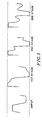
- In a cable equalizer with multiple equalizer stages, each of which clips the signal that it receives to the same, fixed, final level, problems arise in the presence of certain types of input signals. Referring to FIG. 1, if the incoming signal is of good quality, i.e., fairly fast rise times, but an amplitude below the clipping level, the first stage creates an overshoot as it sharpens the high-going transition. This overshoot is clipped, but as it trails off to the correct high level a premature trailing edge is produced. The high frequency gain of the subsequent stages then accentuates this premature trailing edge into a ringing that partially or completely closes the "eye" of the bit interval, causing errors.
- One way to correct this problem is to precede the equalizer with an automatic gain control (AGC) amplifier, see e.g. WO-A-90 13 174, which discloses a system, wherein the gain of a multiplier/amplifier is controlled by calculating the energy value of the input signal. However, this leads to undesirable complexity and excessive power dissipation.
- It is an object of the present invention to provide an alternative way to produce a wide dynamic range of cable equalization in a manner that does not produce overshoots and consequent bit errors, and yet avoids undesirable complexity and excessive power dissipation.
- It is also an object of the present invention to be able to implement the design of the cable equalizer in an integrated circuit (IC) with a minimum of interference between the cable equalization circuitry and other circuitry on the same IC.
- According to this invention there is provided an automatic cable equalizer as claimed in
claim 1 herein. - In the invention, there is provided a multiple section cable equalizer with a signal level detector that produces a clipping control signal for amplifiers in each equalizer section, so that a variable level input signal is restored to an equalized output signal that is undistorted and free of bit errors. A fixed reference clipping stage after the last equalizing stage produces a signal clipped to a final output level. A feedback path limits DC drift in the presence of excess data in either state. A test output stage permits monitoring of the operation of the equalizer stages.
- In a preferred embodiment, the signal level detector contains (in series) a differential amplifier with low pass filtering, a balanced modulator detector, a voltage amplifier, a comparator and peak detector, a transconductance amplifier and a plurality of current mirrors operatively connected to determine a difference current from the output of the transconductance amplifier and convert this to a clipping control signal voltage level. A defeat comparator monitors the output of the comparator and peak detector and replaces the variable difference current with a fixed reference current when an external capacitor used by the peak detector appears to be shorted.
- The subject matter of the present invention is particularly pointed out and distinctly claimed in the concluding portion of this specification. However, both the organization and method of operation, together with further advantages and objects thereof, may best be understood by reference to the following detailed description and accompanying drawings.
-
- FIG. 1 is an illustration of how cable equalizers with fixed clipping thresholds can treat certain types of input signals inappropriately;
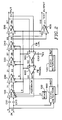
- FIG. 2 is a block diagram of the equalizer portion of the level independent automatic cable equalizer of the present invention;
- FIG. 3 is a block diagram of the level detection portion of the level independent automatic cable equalizer of the present invention;
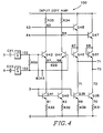
- FIG. 4 is a schematic diagram of the unity gain differential amplifier;
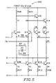
- FIG. 5 is a schematic diagram of one of the three identical equalizer stages;
- FIG. 6 is a schematic diagram of the limiting differential stage with ECL level shift circuitry;
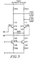
- FIG. 7 is a schematic diagram of the test output stage;
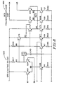
- FIG. 8 is a schematic diagram of the feedback limiting stage and the feedback transconductance amplifier;
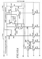
- FIG. 9 is a schematic diagram of the input low pass filter and differential amplifier and the balanced modulator detector;
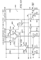
- FIG. 10 is a schematic diagram of the voltage amplifier, the comparator and the peak detector;
- FIG. 11 is a schematic diagram of the voltage reference generator;
- FIG. 12 is a schematic diagram of the transconductance amplifier and two current mirrors;
- FIG. 13 is a schematic diagram of the current mirror and output current source; and
- FIG. 14 is a schematic diagram of the defeat comparator.
- Referring to FIG. 2, a differential input signal, or a single-ended input signal and ground, are applied across DC blocking capacitors CXl and CX2 to the plus and minus inputs of input
differential amplifier 100. Inputdifferential amplifier 100 also receives a fixed reference signal REF fromfixed reference circuitry 140, a BIAS signal frombias circuit 120 and plus and minus sides of a feedback signal. Thedifferential amplifier stage 100 serves to convert any single-ended inputs into differential signals before they reach thefirst equalizer stage 200. Node numbers, such as 5 and 6 on the input to the inputdifferential amplifier 100, can largely be ignored temporarily in the block level discussion which follows immediately, but will prove very useful in tying together the schematic level discussion which follows further below. - The outputs of
differential amplifier 100 are applied to the first of threeidentical equalizer stages equalizer stage level detection circuitry 900. - The differential outputs of the
third equalizer stage 240 are applied to the plus and minus inputs of both limitingdifferential stage 300 andtest output stage 400. Limitingstage 300 andtest output stage 400 both receive the fixed reference signal REF, but not the variable reference signal VREF. Thetest output stage 400 has unity gain and its outputs provide a view for test purposes into the behavior of theequalizer stages limiting stage 300. The output of limitingstage 300 is limited to the full output signal level, regardless of the level of variable limiting that theequalizer stages - The differential outputs of the
limiting stage 300 are also monitored byfeedback limiting stage 500 which operates in response to VREF to limit to the same level as theequalizer stages feedback limiting stage 500 are applied to the plus and minus inputs offeedback transconductance amplifier 600, which produces feedback currents that are then supplied to the unity gaindifferential amplifier stage 100. Thedifferential amplifier stage 100 sums these currents into its output to maintain a suitable DC level in the presence of data containing significantly more of one logic state than another. (This type of feedback circuitry has also sometimes been called "quantized feedback circuitry".) - The variable reference signal VREF is produced by the
level detection circuitry 900, which is shown in detail in FIG. 3. FIG. 3 illustrates a lowpass filteringdifferential amplifier 700 whose inputs are DC coupled to the input signals atnodes differential amplifier 700 are applied to the inputs of abalanced modulator detector 710. Thebalanced modulator detector 710 full-wave rectifies both sides of the signal on its inputs and produces two levels whose difference represents the amplitude of the low frequency component of the input signal. "Low frequency" as used in connection with this invention refers to frequencies below 50 MHz, since this is the highest frequency that is not significantly affected by cable losses. - The output levels from the
balanced modulator detector 710 are applied to differential inputs ofvoltage amplifier 720, which produces a single output voltage that is proportional to the difference in the output levels of thebalanced modulator detector 710. This voltage is applied to a comparator andpeak detector 730. The comparator portion of the comparator andpeak detector 730 provides a fast charging path for the peak detector portion. The peak detection is very fast, but the relaxation of the detected value is relatively very slow. - The output of the comparator and peak detector 730 (node 37) is applied to the input of a
transconductance amplifier 740. Thetransconductance amplifier 740 converts this voltage to a pair of differential currents (nodes 49 and 48). Each of these output currents from thetransconductance amplifier 740 is applied to a current mirror,node 49 tocurrent mirror 750 andnode 48 tocurrent mirror 760. The summer portion of current mirror andsummer 770 sums the current from its internal current mirror, reflecting the current fromcurrent mirror 760, with the current fromcurrent mirror 750 to produce an output current atnode 59 that is equivalent to the difference between the pair of differential currents at the output of the trans-conductance amplifier 740. - The output of current mirror and
summer 770,node 59, is an input to variable referencevoltage output circuitry 800. The variable referencevoltage output circuitry 800 produces a final output voltage VREF that is proportional to the current from the output of the current mirror and summer 770 (node 59). This reference voltage is proportional to the amplitude of the low frequency content of the input signal. -
Fixed voltage generator 780 produces at node 99 a reference voltage required bycurrent mirrors voltage output circuitry 800. - The output of the comparator and peak detector 730 (node 37) is also applied to one of the inputs of
defeat comparator 790. The other input to thedefeat comparator 790 is a reference voltage (node 96) that is generated by a reference voltage generator that is internal to thetransconductance amplifier 740. From these two inputs thedefeat comparator 790 ascertains whether or not the comparator andpeak detector 730 appears to be working properly. If it appears to thedefeat comparator 790 that the comparator andpeak detector 730 is not functioning properly, the defeat comparator shuts off the output (node 59) of the current mirror and summer 770 (via node 50) and causes the variable reference voltage output circuitry 800 (via node 51) to produce a default variable reference VREF that is equal to the fixed reference REF. - Before referring to the schematic level Figures, it will be helpful to define the levels associated with several circuit nodes that are used throughout the various schematics:
TABLE OF COMMON NODE VALUES Node No. Name Typical Voltage 0 VEE 0.0 V 1 VCC +5.0 V 102,103 BIAS +2.75 V 3 REF +0.6 V + V BE4 VREF +0.3 V + VBE
to +1.2 V + VBE - Referring now to FIG. 4 in conjunction with FIG. 2, the input signal is AC coupled through the external capacitors CXl and CX2, and applied to the inputs of a differential amplifier comprising transistors Q42 and Q43. The value of R29 in conjunction with values of the collector resistors R35 and R34 establishes the gain to be approximately unity. The bases of the differential pair Q42 and Q43 are biased to 2.75 Volts by BIAS signals on
nodes node 3 establishes the maximum current available to the emitters of differential amplifier pair Q42,Q43. - As will be further explained below, the currents on
nodes feedback transconductance amplifier 600, are summed with the currents from the collectors of Q42 and Q43, respectively, by the collector resistors R35 and R34, to produce the actual output voltages of the differential pair. When the input data has on average as many ones as zeros, the currents supplied tonodes nodes differential amplifier stage 100 atnodes - Referring now to FIG. 5, a schematic diagram of the
first equalizer stage 200, the outputs from thedifferential amplifier stage 100 appearing onnodes equalizer stage 200 is significantly increased, becoming about 10 dB at frequencies around 135 MHz; 135 MHz being the theoretical minimum bandwidth for DI. (DI is the fastest of the current video standards.) - The maximum current available to the transistors Q34,Ql0 of the differential pair, and therefore the maximum output voltages that can be developed across the collector resistors R25 and R24, is determined by the variable reference voltage, VREF. The output voltages from the differential pair Q34,Q10 are buffered and level shifted down two base-emitter voltage drops by Q33,Q9 and Q14,Q7, respectively, to produce the final output of the
equalizer stage 200. The second and third equalizer stages 220 and 240 are identical to thefirst equalizer stage 200. The overall equalizer with three stages provides up to 30 dB of high frequency signal boosting, capable of compensating for the high frequency losses due to 300 meters of cable. - Referring now to FIG. 6 in conjunction with FIG. 2, the output of the
third equalizer stage 240 is presented to the limitingstage 300 atnodes stage 300 are directly coupled together, so that these transistors operate as a switch to switch the current from Q49 between the collector resistors R40 and R39 to produce an output that has minimum rise and fall times. Q49 is controlled by the fixed reference voltage REF onnode 3, and the relative values of its emitter resistor R37 and the collector resistors R40 and R39 of transistors Q59 and Q5l are selected to produce the desired ECL output level swing of the final output of the overall cable equalizer. As in the preceding stages, the output voltage swings of this differential amplifier are then buffered and level shifted down two base-emitter voltage drops by Q52,Q54 and Q59,Q55 to produce the output signals atnodes nodes - Referring to FIG. 7, as well as FIG. 2, the output of the
third equalizer stage 240 is also presented to thetest output stage 400 atnodes - Referring now to FIG. 8 in conjunction with FIG. 2, the output of the limiting
stage 300, atnodes feedback limiting stage 500.Nodes - A second current source formed by Q63 and R65 is controlled by the variable reference signal VREF. The voltage developed across R46 by the current from the latter current source is applied to the base of another emitter follower Q72. The emitters of Q73 and Q72 are connected to the bases of a differential pair of transistors Q62 and Q60, respectively, which form the
feedback transconductance amplifier 600. Note that R45 is twice as large as R44. - To illustrate the operation of the
feedback limiting stage 500 andtransconductance amplifier 600, let us first imagine that the NRZ data passing through the cable equalizer has been a long string of one, zero, one, zero, etc. Under these contitions Q64 is fully conducting half of the time. Because R44 is half of the size of R45, the average current through Q64 is the same as the constant current through Q63. The RC time of CX3 and R47 is long compared with the bit data rate, so the voltage on CX3 and the base of Q73 is equal to the voltage on the base of Q72. Therefore, under these circumstances, the currents through Q62 and Q60 of thefeedback transconductance amplifier 600 are balanced and no net steering of the DC level of the output of the inputdifferential amplifier 100 connected tonodes - When different data arrives, such as one, one, zero, one, one, zero, etc., the average current through Q64 will differ from the current through Q63, and the charge on CX3 and the voltage on the base of Q73 will become different from the constant voltage on the base of Q72. The resulting voltage difference of the bases of Q62 and Q60 will cause a difference in the currents being supplied to
nodes differential amplifier 100 occurs. In this way, the difference current supplied by thefeedback transconductance amplifier 600 restores any DC component lost by AC coupling through coupling capacitors CX1 and CX2 at the input of the inputdifferential amplifier 100. - For correct restoration of the DC component lost by AC coupling through capacitors CX1 and CX2, the time constant of CX3 and R47 should be equal to the time constant associated with CX1, CX2, R58 (FIG. 4) and the two 18000 Ohm bias source resistors (not shown), and the loop gain through the feedback path should be near unity. In this implementation, the time constants of both of these circuits correspond to a frequency of about 2 MHz and the loop gain is about 0.9. The loop gain is determined by the selection of the value of R43 between the emitters of Q62 and Q60. In practice it is prudent to design toward a gain of about 0.9, rather than 1.0, since it is safer to under-compensate than to over-compensate, given that an amplifier with a gain in excess of 1.0 may become unstable and process and temperature variations must be anticipated and guarded against.
- FIGS. 9 through 14 illustrate in schematic diagrams the circuitry shown in block diagram form in FIG. 3, all of which is shown as
block 900 in FIG. 2. The node numbers in FIGS. 9 through 14 in many cases duplicate the node numbers used in FIGS. 4 through 8, but they are different and should not be confused with their counterparts in the other set of schematics. - Referring to FIG. 9, the input low-pass filtering
differential amplifier stage 700 is DC coupled to the input signal onnodes - The differential amplifier consisting of Q50 and Q49 has about unity gain, its main function being to ensure for the circuitry downstream that the input signal is differential in the event that the input is being driven by a single-ended signal. The outputs of this stage are buffered and dropped one base-emitter voltage by Q55 and Q54 and input (at
nodes 15 and 16) to the upper portion of thebalanced modulator detector 710, consisting of switching differential pairs Q36,Q37 and Q38,Q39. These outputs of the input low-pass filtering differential amplifier stage Q50,Q49 are further dropped an additional two base-emitter voltages by diode connected transistors Q48,Q46 and Q47,Q45, and then applied (atnodes 19 and 20) to the inputs of a current modulating differential pair Q42,Q33. The current outputs of the balanced modulator detector (atnodes 27 and 28) are full-wave rectified versions of the input signals. These are then buffered and dropped two base-emitter voltage drops by emitter followers Q35 and Q66 and diode connected transistors Q74 and Q69, and then appear athigh output node 77 andlow output node 80. - Referring next to FIG. 10, as well as FIG. 3, the outputs of the
balanced modulator detector 710,nodes voltage amplifier 720 on the bases of transistors Q70 and Q68. The voltage amplifier develops its output across resistor R36. The voltage developed across the 4K resistor R36 is applied to the base of transistor Q77 through 50K resistor R42. Emitter follower transistor Q77 buffers this signal and drops it by one base-emitter voltage drop and applies it to the base of transistor Q60, one side of the comparator portion of comparator andpeak detector 730. - The other side of the comparator, transistor Q6l, receives its input from the
node 36 output of the peak detector portion of the comparator andpeak detector 730.Node 36 is the emitter of emitter follower transistor Q53 whose base is connected to VCC through a 50K resistor R43 and a 4K resistor R12. Note that these resistors on the base of Q53 have the same values as the resistors on the base of Q77. The matching of these resistors within the same IC process ensures that even in the presence of process and temperature variations, the relative resistance in the base circuits of transistors Q53 and Q77 will remain equivalent. - The comparator Q60,Q61 is then monitoring and comparing the output of the voltage amplifier at
node 79 with the charge on the external 200 pF capacitor CX4 atnode 32 in the peak detector. When the voltage atnode 86 is more positive than the voltage atnode 32, Q60 conducts and Q6l does not. Thus,node 66 is lower thannode 67, and these relative voltages, after they are buffered and dropped two base-emitter voltage drops through emitter followers Q58 and Q57 and diode connected transistors Q59 and Q56, cause Q30 to be shut off and the current from Q29 to go through Q3l, and the charge on CX4 to remain approximately the same. - When the voltage from the voltage amplifier at
node 86 becomes more negative than the charge on CX4, Q61 conducts and Q60 does not.Node 67 is then lower thannode 66, causing Q31 to shut off and the current from Q29 to go through Q30, charging CX4. The detected peak output voltage is buffered and dropped one base-emitter voltage drop by emitter follower Q53 to provide the signal to the base of Q61, and dropped another base-emitter voltage drop by diode connected transistor Q21 to produce the output of the comparator andpeak detector 730 atnode 37. - The discharge path for CX4 through the 54K resistance path of resistors R43 and R12 is quite slow compared with the data being monitored. The RC time of this 200 pF, 54K Ohm discharge path is 10.8 microseconds, compared with the incoming data rate of about 100 MHz (10 ns). Transistors Q29 and Q30 each have a large emitter area and therefore have a low emitter resistance. Consequently, the RC time of the charging path of CX4 is determined by the 700 Ohm emitter resistor of Q29 and is about 140 ns. Thus, the peak detector is fast attack and slow release.
- When there is no signal input to
nodes node 77 andnode 80 inputs to thevoltage amplifier 720 are in balance and the current available to Q70 is determined by REF onnode 3. Recalling that REF is 0.6 Volts plus one base-emitter voltage, the voltage across R38 on the emitter of transistor Q72 is 0.6 Volts and the current that flows is about 214 uA. That current produces a voltage drop of about 0.86 Volts across R36 with its 4K Ohm value. The comparator andpeak detector 730 then ensure that that voltage is also maintained on CX4. - Referring now to FIG. 11 as well as FIG. 3, the fixed
voltage generator 780 produces a reference voltage from current source transistor Q131 and its emitter resistor R93 that is two base-emitter voltage drops down from VCC as a result of diode connected transistors Q128 and Q147. Capacitor C2 provides some decoupling to ground. This reference voltage is supplied tocurrent mirrors voltage output circuitry 800 which also contains a current mirror. - Referring now to FIG. 12 as well as FIG. 3, the
node 37 output of the comparator andpeak detector 730 is the input totransconductance amplifier 740 on the base of Q18. The other side of differential pair Q18,Q17, the base of transistor Q17, receives a locally derived reference voltage generated by the application of the current from transistor Q24 and its emitter resistor R27 to the 4K collector path consisting of the two 2K resistors R48 and R5, after it has been buffered and dropped two base-emitter voltage drops by emitter follower Q22 and diode connected transistor Q15. - Note that the circuit composed of transistor Q24, emitter resistor R27, collector resistors R5 and R48 and emitter follower Q22 with its base resistor R44 closely matches, with respect to resistance values and emitter areas, the circuit in the voltage amplifier 720 (FIG. 10) composed of transistors Q70 and Q72, emitter resistor R38, collector resistor R36 and emitter follower Q77 with its base resistor R42. Therefore, when produced within the same IC and process these two circuits will be well matched, even in the presence of process and temperature variations.
- Referring now to FIG. 10 as well as FIG. 12, if no input signal is present, the operation of the comparator and
peak detector 730drives node 36 to the same voltage level asnode 87. Sincenode 37 is one base-emitter voltage drop belownode 36 andnode 45 is one base-emitter voltage drop belownode 44,nodes transconductance amplifier 740 are balanced. Further,node 43 will be at the same voltage level asnode 86, or -0.86 V relative to VCC, andnode 96 will be at -0.43 V relative to VCC. - When a signal input is present, the voltage on
node 37 will vary in proportion to the level of the low frequency component of that signal, as described above, and theother node 45 of thetransconductance amplifier 740 will remain fixed at the level that was present in the absence of a signal. Accordingly, the current output onnode 49 to PNPcurrent mirror 750 will increase, while the current output onnode 48 to PNPcurrent mirror 760 decreases by the same amount. - The bases of both Ql40 on the right side of PNP
current mirror 750 and Ql36 on the right side of PNPcurrent mirror 760 are connected to the output of the fixedvoltage generator 780 onnode 99. Looking for example at the first PNPcurrent mirror 750, as the current throughnode 49 increases, the differential pair Q144 and Q140 operates to increase conduction through Q142 causing both of the PNP transistors, Q143 and Q142, to turn on to holdnode 49 at the same voltage as the reference onnode 99. Thus, the output current throughnode 60 increases, mirroring the current innode 49. - The output of the first PNP
current mirror 750 is one input to the NPNcurrent mirror 770. As the voltage on the base of transistor Q34 attempts to change in response to changing current throughnode 60, this change is transmitted by the emitter following action of Q34 to the base of transistor Q8, which in response alters its conduction to permit the new amount of current to flow. Because the base of transistor Q7 is tied to the same node (29) as the base of transistor Q8 and both transistors have the same emitter areas, a current is produced through Q7 that is the same as the current through Q8. - The second PNP
current mirror 760 operates in the same way as the first PNPcurrent mirror 750, producing a current atnode 58 that is the same as the current atnode 48. The output of the second PNPcurrent mirror 760 is applied tonode 58, where it is partially cancelled by the current from the NPN current mirror output transistor Q7. The difference in these two currents is supplied by a diode connected transistor Q135, since transistor Q152 is normally off. Thenode 59 current that flows through Ql35 is the difference between the two current outputs of thetransconductance amplifier 740, and provides the input to the variable referencevoltage output circuitry 800. - In a semiconductor process that is generally optimized for NPN transistors, PNP transistors can best be implemented as lateral PNP transistors. However, lateral PNP transistors are typically slow and have low beta values. In the process used for an actual implementation, a beta of 20 was achieved, but the low speed of the lateral PNP transistors tended to cause oscillations. To eliminate this tendency,
current mirror 750 includes a pole-zero compensation network consisting of R105 and C4. The exact optimum values used for this network depend on process details and the exact type of NPN transistors being employed. Resistor R98 provides a path for the collector current of Q142 so that the currents through the differential pair Q144 and Q140 are more closely matched. Otherwise, the only current on the Q142 side would be the emitter currents of the PNP transistors Q143 and Q142. R98 also contributes to the stability of the circuit's operation, and thereby assists the compensation network of R105 and C4 in preventing oscillations. - Referring now to FIG. 13 as well as FIG. 3, the
node 59 input to the variable referencevoltage output circuitry 800 is applied to one side of an amplifying NPNcurrent mirror 810 that produces the variable reference voltage output VREF. This current flows through transistor Q5 under the control of feedback through emitter follower transistor Q65 and a current 25% larger flows through transistor Q6 due to the relationship between the values of resistors R2 and Rl. The VREF output, which is the voltage on the bases of the NPN current mirror transistors Q5 and Q6, appears onnode 75. The output voltage VREF is the voltage developed across R2 by the difference current onnode 59 plus one VBE. - For a nominal input voltage 0.8 Volt peak-to-peak on
nodes node 75, the VREF output. For the maximum expected peak-to-peak input voltage of 1.6 Volts the output is 1.2 Volts plus one VBE. And, for the minimum input signal of 0.4 Volts peak-to-peak the output is 0.3 Volts plus one VBE. In general, VREF = 3/4*VIN + VBE. - The variable reference
voltage output circuitry 800 also includes a PNPcurrent mirror 805, the operation of which will be described in connection with the discussion of FIG. 14. - Referring to FIG. 14 and to FIG. 3, the
defeat comparator 790 compares the voltage onnode 37 with that onnode 111, which is the voltage level onnode 96 dropped two base-emitter voltage drops by emitter follower transistor Q78 and diode connected transistor Q79.Node 37 is the peak detector output at node 32 (see FIG. 10) dropped two base-emitter voltage drops. Thus, a comparison betweennodes nodes - If
node 37 is more negative thannode 111, which will always be the case in normal operation, Q80 will conduct and Q81 will not. The higher voltage on the base of Q149 causes it to shut off, while the lower voltage on the base of Q150 causes it to conduct. With Q149 off, the voltage onnode 50 goes low, while with Q150 on, the voltage onnode 51 goes high. - Referring now to FIG. 12, the low voltage level on
node 50 keeps Q152 off and current flows through Q135 andnode 59 normally, as described above. Referring now to FIG. 13, the high voltage level onnode 51 keeps Q151 turned on and the output of the PNPcurrent mirror 805 in the variablevoltage output circuitry 800 is shunted tonode 0, VEE. - Referring now to FIGS. 10, 12 and 14, the only time that
node 37 will be positive relative tonode 111 is if the external capacitor is shorted to VCC, either intentionally or inadvertently. When this has occurred, the situation just described is reversed. That is,node 50 goes high andnode 51 goes low. A high onnode 50 causes Q152 to conduct causing the summed currents from the threecurrent mirrors node 51 shuts off Q151 eliminating the shunt path for the current from the PNPcurrent mirror 805. With this shunt path eliminated, the current being produced by Q134 in the PNP current mirror flows through diode connected transistor Q127. - The base of Q87 is biased with the fixed reference voltage REF at 0.6 Volts plus one base-emitter drop voltage. That causes the emitter of Q87 to produce 0.6 Volts, which causes 125 uA to flow through R76, the 4800 Ohm emitter resistor. The flow of this 125 uA through the 20K Ohm collector resistor R62 provides a bias voltage on the base of Q93 that is -2.5 Volt relative to VCC. The base of Ql08, the other side of that differential pair, is tied to the collector of output transistor Q6, which is identical in its size and its emitter and collector resistor values with Q87. Thus, the differential pair Q93 and Q108 will only be in balance when the current through Q6 equals the current through Q87. The output of the differential pair Q93 and Q108 regulates the current through Q6 necessary to achieve this balance via the output of the PNP current mirror consisting of transistors Q133, Q132, Q138 and Q134 and its output path through diode connected transistor Q127 and the other side of the amplifying NPN
current mirror 810 that Q6 is part of. - Thus, when the output of the
defeat comparator 790 switches to the "defeat" state, indicating that the external capacitor CX4 has been shorted, this PNPcurrent mirror 805 causes the variable reference voltage VREF to go to the same voltage level as the fixed voltage reference REF, i.e., 0.6 Volts plus one base-emitter voltage drop. - By relying on the use of the ratios between resistors, rather than the absolute values of resistors, the design described above is made robust in the face of process and temperature variations.
- By the use of variable clipping levels, as derived and applied above, the automatic cable equalizer of the present invention is able to accept a variable input signal and produce an equalized output signal that is free of distortion and attendant bit errors.
- While a preferred embodiment of the present invention has been shown and described, it will be apparent to those skilled in the art that many changes and modifications may be made without departing from the invention in its broader aspects. The claims that follow are therefore intended to cover all such changes and modifications as fall within the true scope of the invention.
Claims (10)
- An automatic cable equalizer for compensating for a variable level input signal (5, 6) with possibly degraded rise and fall times, the automatic cable equalizer being of the type having multiple equalizer stages (200, 220, 240), wherein:each equalizer stage (200, 220, 240) has an input and an output, with the input coupled to the output of the prior equalizer stage, the input of the first equalizer stage (200) being coupled to receive the variable level input signal and the output of the last equalizer stage (240) providing an equalized signal for the variable level input signal, each equalizer stage further contains amplifying means (Q34, Q10), high frequency gain boosting means (R7, C1, R8) and clipping means with the clipping means having a clipping control input (4) coupled to receive a clipping control signal; andsignal level detecting means (700-800) are coupled to monitor the variable level input signal and for producing the clipping control signal, the clipping control signal being proportional to the peak level of the rectified low frequency content of the variable level input signal (5, 6).
- An automatic cable equalizer according to claim 1 further comprising:an AC coupling capacitor (CX1,CX2) coupled to the equalizer input (5,6); andfeedback means (500,600,CX3) having an input and an output, with the input (87,88) coupled to receive the output of the equalizer section and with the output (64,63) coupled to restore the DC lost by AC coupling.
- An automatic cable equalizer according to claim 2, wherein an RC time (CX1,R58,R49,R50,CX2) associated with the AC coupling capacitor is approximately equal to an RC time (R47,CX3) associated with the feedback means (500,600,CX3).
- An automatic cable equalizer according to claim 1 further comprising a limiting section (300) having an input and an output, with the input coupled to receive the output (21,22) of the equalizer section (200), the limiting section limiting to a fixed (3) clipping level.
- An automatic cable equalizer according to claim 1 further comprising a test output stage (400) having approximately unity voltage gain, a high impedance input and a low impedance output, with the input coupled to the output of the equalizer (21,22).
- An automatic cable equalizer according to claim 1, wherein the signal level detecting means (700-800) comprises:low pass filtering means (700) coupled to receive the variable level input signal (5,6) and produce a low frequency content signal (13,14);rectifying means (710,720) coupled to receive the low frequency content signal (13,14) and producing a rectified low frequency content signal (87);peak holding means (730,CX4) coupled to receive the rectified low frequency content signal (87) and producing a maximum low frequency content signal (37); andscaling means (740-800) coupled to receive the maximum low frequency content signal (37) and producing the clipping control signal (4) proportionally to the maximum low frequency content signal (37).
- An automatic cable equalizer according to claim 6, wherein the peak holding means (730) comprises:charge storing means (CX4) for holding a peak charge;comparator means (Q60,Q61) having a first input (87), a second input (36) and an output (70,71), with the first input (87) coupled to receive the rectified low frequency content signal and the second input coupled to receive an indication of the peak charge (32), the output (70,71) indicating when the first input is larger than the second input; andcharge adding means (Q31,Q30) responsive to the output (70,71) of the comparator means (Q60,Q61) for adding to the peak charge (CX4) when the rectified low frequency content signal (87) exceeds the present peak charge.
- An automatic cable equalizer according to claim 6, wherein the scaling means (740-800) comprises:transconductance amplifying means (740-770) having an input and an output, the input being coupled to receive the maximum low frequency content signal (37) and the output (59) being a current proportional to the magnitude of the maximum low frequency content signal (37); andsignal producing means (800) for receiving the output current (59) from the transconductance amplifier (740) and producing the clipping control signal (4) proportionally to the received output current (59).
- An automatic cable equalizer according to claim 8, wherein the transconductance amplifying means (750-770) comprises:a transconductance amplifier (740) having an input and two outputs, the input being coupled to receive the maximum low frequency content signal (37) and the outputs (48,49) being two currents whose difference is proportional to the magnitude of the maximum low frequency content signal (37); anda plurality of current mirrors (750,760,770) receiving the output currents (48,49) from the transconductance amplifier (740) operatively connected (60,58) to establish the difference current (59).
- An automatic cable equalizer according to claim 8, wherein the scaling means further comprises defeat comparator means having first and second inputs and an output, with the first input coupled to receive the maximum low frequency content signal (37) and the second input coupled to receive a reference signal (96), and producing at the output a selection signal (50,51) selecting the difference current (59) or a fixed current (800) as a basis for establishing the level of the clipping control signal (4).
Applications Claiming Priority (2)
| Application Number | Priority Date | Filing Date | Title |
|---|---|---|---|
| US691898 | 1991-04-26 | ||
| US07/691,898 US5124673A (en) | 1991-04-26 | 1991-04-26 | Level independent automatic cable equalizer |
Publications (3)
| Publication Number | Publication Date |
|---|---|
| EP0510976A2 EP0510976A2 (en) | 1992-10-28 |
| EP0510976A3 EP0510976A3 (en) | 1993-07-07 |
| EP0510976B1 true EP0510976B1 (en) | 1997-05-28 |
Family
ID=24778417
Family Applications (1)
| Application Number | Title | Priority Date | Filing Date |
|---|---|---|---|
| EP92303664A Expired - Lifetime EP0510976B1 (en) | 1991-04-26 | 1992-04-23 | Level independent automatic cable equalizer |
Country Status (5)
| Country | Link |
|---|---|
| US (1) | US5124673A (en) |
| EP (1) | EP0510976B1 (en) |
| JP (1) | JPH0662273A (en) |
| CA (1) | CA2063350A1 (en) |
| DE (1) | DE69219947T2 (en) |
Families Citing this family (28)
| Publication number | Priority date | Publication date | Assignee | Title |
|---|---|---|---|---|
| US5483552A (en) * | 1992-10-27 | 1996-01-09 | Matsushita Electric Industrial Co., Ltd. | Adaptive equalizing apparatus for controlling the input signal level of quantized feedback |
| KR0157711B1 (en) * | 1995-07-12 | 1998-11-16 | 김광호 | Equalizing method in data communication terminal |
| US5978417A (en) * | 1996-02-23 | 1999-11-02 | National Semiconductor Corporation | Adaptive cable equalizer |
| US5708389A (en) * | 1996-03-15 | 1998-01-13 | Lucent Technologies Inc. | Integrated circuit employing quantized feedback |
| US6150875A (en) * | 1998-04-17 | 2000-11-21 | Advanced Micro Devices, Inc. | Apparatus and method for equalizing received network signals using a transconductance controlled single zero single pole filter |
| JP3948116B2 (en) * | 1998-05-11 | 2007-07-25 | ソニー株式会社 | DC recovery circuit |
| US6259302B1 (en) * | 1998-10-22 | 2001-07-10 | National Semiconductor Corporation | Gain control signal generator that tracks operating variations due to variations in manufacturing processes and operating conditions by tracking variations in DC biasing |
| US6466626B1 (en) | 1999-02-23 | 2002-10-15 | International Business Machines Corporation | Driver with in-situ variable compensation for cable attenuation |
| CA2368432C (en) * | 1999-04-06 | 2008-08-12 | Adc Telecommunications, Inc. | Dsx module with removable jack |
| US7031420B1 (en) * | 1999-12-30 | 2006-04-18 | Silicon Graphics, Inc. | System and method for adaptively deskewing parallel data signals relative to a clock |
| US6956905B1 (en) * | 2000-03-23 | 2005-10-18 | Xilinx, Inc. | Peak detector circuit |
| US6490466B1 (en) * | 2000-09-21 | 2002-12-03 | Mallinckrodt Inc. | Interconnect circuit between non-compatible oximeter and sensor |
| DE10142612A1 (en) * | 2001-08-31 | 2003-04-03 | Siemens Ag | Method and device for single-core, local transmission of PCM signals without a transmitter |
| US20030099307A1 (en) * | 2001-11-13 | 2003-05-29 | Narad Networks, Inc. | Differential slicer circuit for data communication |
| US6784698B1 (en) * | 2003-06-11 | 2004-08-31 | Agere Systems Inc. | Sense amplifier with improved common mode rejection |
| US7620121B1 (en) | 2004-12-09 | 2009-11-17 | Xilinx, Inc. | DC balance compensation for AC-coupled circuits |
| US7961817B2 (en) * | 2006-09-08 | 2011-06-14 | Lsi Corporation | AC coupling circuit integrated with receiver with hybrid stable common-mode voltage generation and baseline wander compensation |
| US8213638B2 (en) * | 2007-02-20 | 2012-07-03 | Texas Instruments Incorporated | Equalizer |
| US8085839B2 (en) * | 2007-08-01 | 2011-12-27 | Gennum Corporation | Adaptive equalization system and method having a lock-up-free quantized feedback DC restoration circuit |
| TWI392364B (en) * | 2008-02-29 | 2013-04-01 | Analog Devices Inc | Feedback system and apparatus for video compensation |
| US8335249B1 (en) * | 2009-11-25 | 2012-12-18 | Altera Corporation | Receiver equalizer circuitry with offset voltage compensation for use on integrated circuits |
| US8295336B2 (en) * | 2010-03-16 | 2012-10-23 | Micrel Inc. | High bandwidth programmable transmission line pre-emphasis method and circuit |
| US8379702B2 (en) * | 2010-03-16 | 2013-02-19 | Micrel, Inc. | High bandwidth programmable transmission line pre-emphasis method and circuit |
| US8379701B2 (en) * | 2010-03-16 | 2013-02-19 | Micrel, Inc. | High bandwidth dual programmable transmission line pre-emphasis method and circuit |
| US8817863B2 (en) * | 2011-02-09 | 2014-08-26 | Rambus Inc. | Linear equalizer with passive network and embedded level shifter |
| US9661248B2 (en) * | 2013-12-13 | 2017-05-23 | Cista System Corp. | Integrated circuit having flexible reference |
| JP6226945B2 (en) * | 2015-12-11 | 2017-11-08 | アンリツ株式会社 | Multiband equalizer, error rate measurement system using the same, error rate measurement device, and path selection method |
| US10063253B1 (en) * | 2017-06-22 | 2018-08-28 | Intel Corporation | Summer circuit including linearized load |
Citations (1)
| Publication number | Priority date | Publication date | Assignee | Title |
|---|---|---|---|---|
| US534016A (en) * | 1895-02-12 | smithley |
Family Cites Families (8)
| Publication number | Priority date | Publication date | Assignee | Title |
|---|---|---|---|---|
| US3529244A (en) * | 1967-03-13 | 1970-09-15 | Columbia Broadcasting Syst Inc | Method and apparatus for frequency sensitive amplitude limiting |
| US3568100A (en) * | 1967-12-26 | 1971-03-02 | Bell Telephone Labor Inc | Automatic equalizer for digital transmission systems |
| JPS5313927B2 (en) * | 1971-12-31 | 1978-05-13 | ||
| US3983381A (en) * | 1974-12-18 | 1976-09-28 | International Business Machines Corporation | Digital automatic gain control circuit |
| FR2520174A1 (en) * | 1982-01-15 | 1983-07-22 | Lignes Telegraph Telephon | SYSTEM FOR TRANSMITTING DIGITAL SIGNALS ON OPTICAL FIBER |
| US4606043A (en) * | 1984-10-09 | 1986-08-12 | At&T Bell Laboratories | Programmable automatic cable equalizer |
| JPS63316571A (en) * | 1987-06-19 | 1988-12-23 | Sony Corp | Video signal processing circuit |
| US5016205A (en) * | 1989-04-27 | 1991-05-14 | Motorola, Inc. | Digital signal processor based AGC |
-
1991
- 1991-04-26 US US07/691,898 patent/US5124673A/en not_active Expired - Lifetime
-
1992
- 1992-03-18 CA CA002063350A patent/CA2063350A1/en not_active Abandoned
- 1992-04-23 DE DE69219947T patent/DE69219947T2/en not_active Expired - Fee Related
- 1992-04-23 EP EP92303664A patent/EP0510976B1/en not_active Expired - Lifetime
- 1992-04-25 JP JP4131876A patent/JPH0662273A/en active Pending
Patent Citations (1)
| Publication number | Priority date | Publication date | Assignee | Title |
|---|---|---|---|---|
| US534016A (en) * | 1895-02-12 | smithley |
Also Published As
| Publication number | Publication date |
|---|---|
| DE69219947T2 (en) | 1997-11-20 |
| US5124673A (en) | 1992-06-23 |
| EP0510976A2 (en) | 1992-10-28 |
| EP0510976A3 (en) | 1993-07-07 |
| JPH0662273A (en) | 1994-03-04 |
| CA2063350A1 (en) | 1992-10-27 |
| DE69219947D1 (en) | 1997-07-03 |
Similar Documents
| Publication | Publication Date | Title |
|---|---|---|
| EP0510976B1 (en) | Level independent automatic cable equalizer | |
| US6501792B2 (en) | Serial digital data communications receiver with improved automatic cable equalizer, AGC system, and DC restorer | |
| US5699386A (en) | System and method for data signal communication using a high-pass function before a low-pass function with quantized feedback technique | |
| JPH08223228A (en) | Equalization amplifier and receiver and preamplifier using same | |
| EP0656164B1 (en) | Television receiver | |
| US5337091A (en) | Video IF amplifier with auxiliary IF amplifier for intercarrier sound & AFT | |
| KR0183114B1 (en) | Using d-c feedback with on-chip filtering to balance i-f drive to second detector in monolithic ic | |
| US5140603A (en) | Overmodulation protection for amplitude modulated laser diode | |
| US5717716A (en) | Quasi-adaptive analog equalization method and apparatus | |
| US4851911A (en) | Video signal noise reduction circuit | |
| US3205442A (en) | Automatic adjustable equalizer for signal amplitude variations | |
| US4156854A (en) | Differential amplifier balancing system | |
| US3829626A (en) | Telephone line equalizer | |
| US7769057B2 (en) | High speed serial link output stage having self adaptation for various impairments | |
| EP0640256B1 (en) | Local area network amplifier for twisted pair lines | |
| US4281346A (en) | Complementary pre-emphasis and de-emphasis circuits for a video signal transfer channel | |
| US4306256A (en) | Preemphasis and clipping apparatus for reducing distortions | |
| EP0271954A2 (en) | Television signal processing apparatus including rise time normalization and noise reduction | |
| US4388647A (en) | Predictably biased DC coupled video signal peaking control system | |
| EP1445903A2 (en) | Serial digital data communications receiver with improved automatic cable equalizer and DC restorer | |
| GB2044587A (en) | Preemphasis and clipping apparatus for reducing distortions | |
| JPH01137468A (en) | Digital signal restoring circuit | |
| CA2283916A1 (en) | Serial digital data communications receiver with improved automatic cable equalizer, agc systems and dc restorer | |
| JPS589415A (en) | Automatic equalizer | |
| JPH06276489A (en) | Dropout detector |
Legal Events
| Date | Code | Title | Description |
|---|---|---|---|
| PUAI | Public reference made under article 153(3) epc to a published international application that has entered the european phase |
Free format text: ORIGINAL CODE: 0009012 |
|
| AK | Designated contracting states |
Kind code of ref document: A2 Designated state(s): DE ES FR GB |
|
| PUAL | Search report despatched |
Free format text: ORIGINAL CODE: 0009013 |
|
| AK | Designated contracting states |
Kind code of ref document: A3 Designated state(s): DE ES FR GB |
|
| 17P | Request for examination filed |
Effective date: 19930621 |
|
| 17Q | First examination report despatched |
Effective date: 19960115 |
|
| GRAG | Despatch of communication of intention to grant |
Free format text: ORIGINAL CODE: EPIDOS AGRA |
|
| GRAH | Despatch of communication of intention to grant a patent |
Free format text: ORIGINAL CODE: EPIDOS IGRA |
|
| GRAH | Despatch of communication of intention to grant a patent |
Free format text: ORIGINAL CODE: EPIDOS IGRA |
|
| GRAA | (expected) grant |
Free format text: ORIGINAL CODE: 0009210 |
|
| AK | Designated contracting states |
Kind code of ref document: B1 Designated state(s): DE ES FR GB |
|
| PG25 | Lapsed in a contracting state [announced via postgrant information from national office to epo] |
Ref country code: FR Effective date: 19970528 Ref country code: ES Free format text: THE PATENT HAS BEEN ANNULLED BY A DECISION OF A NATIONAL AUTHORITY Effective date: 19970528 |
|
| REF | Corresponds to: |
Ref document number: 69219947 Country of ref document: DE Date of ref document: 19970703 |
|
| EN | Fr: translation not filed | ||
| PLBE | No opposition filed within time limit |
Free format text: ORIGINAL CODE: 0009261 |
|
| STAA | Information on the status of an ep patent application or granted ep patent |
Free format text: STATUS: NO OPPOSITION FILED WITHIN TIME LIMIT |
|
| 26N | No opposition filed | ||
| PGFP | Annual fee paid to national office [announced via postgrant information from national office to epo] |
Ref country code: GB Payment date: 19990323 Year of fee payment: 8 |
|
| PGFP | Annual fee paid to national office [announced via postgrant information from national office to epo] |
Ref country code: DE Payment date: 19990326 Year of fee payment: 8 |
|
| PG25 | Lapsed in a contracting state [announced via postgrant information from national office to epo] |
Ref country code: GB Free format text: LAPSE BECAUSE OF NON-PAYMENT OF DUE FEES Effective date: 20000423 |
|
| GBPC | Gb: european patent ceased through non-payment of renewal fee |
Effective date: 20000423 |
|
| PG25 | Lapsed in a contracting state [announced via postgrant information from national office to epo] |
Ref country code: DE Free format text: LAPSE BECAUSE OF NON-PAYMENT OF DUE FEES Effective date: 20010201 |