EP0510895B1 - Information processor - Google Patents
Information processor Download PDFInfo
- Publication number
- EP0510895B1 EP0510895B1 EP92303508A EP92303508A EP0510895B1 EP 0510895 B1 EP0510895 B1 EP 0510895B1 EP 92303508 A EP92303508 A EP 92303508A EP 92303508 A EP92303508 A EP 92303508A EP 0510895 B1 EP0510895 B1 EP 0510895B1
- Authority
- EP
- European Patent Office
- Prior art keywords
- deflection
- recording medium
- probe
- cantilever
- elastic member
- Prior art date
- Legal status (The legal status is an assumption and is not a legal conclusion. Google has not performed a legal analysis and makes no representation as to the accuracy of the status listed.)
- Expired - Lifetime
Links
Images


Classifications
-
- G—PHYSICS
- G11—INFORMATION STORAGE
- G11B—INFORMATION STORAGE BASED ON RELATIVE MOVEMENT BETWEEN RECORD CARRIER AND TRANSDUCER
- G11B9/00—Recording or reproducing using a method not covered by one of the main groups G11B3/00 - G11B7/00; Record carriers therefor
- G11B9/12—Recording or reproducing using a method not covered by one of the main groups G11B3/00 - G11B7/00; Record carriers therefor using near-field interactions; Record carriers therefor
- G11B9/14—Recording or reproducing using a method not covered by one of the main groups G11B3/00 - G11B7/00; Record carriers therefor using near-field interactions; Record carriers therefor using microscopic probe means, i.e. recording or reproducing by means directly associated with the tip of a microscopic electrical probe as used in Scanning Tunneling Microscopy [STM] or Atomic Force Microscopy [AFM] for inducing physical or electrical perturbations in a recording medium; Record carriers or media specially adapted for such transducing of information
- G11B9/1418—Disposition or mounting of heads or record carriers
- G11B9/1427—Disposition or mounting of heads or record carriers with provision for moving the heads or record carriers relatively to each other or for access to indexed parts without effectively imparting a relative movement
-
- G—PHYSICS
- G11—INFORMATION STORAGE
- G11B—INFORMATION STORAGE BASED ON RELATIVE MOVEMENT BETWEEN RECORD CARRIER AND TRANSDUCER
- G11B9/00—Recording or reproducing using a method not covered by one of the main groups G11B3/00 - G11B7/00; Record carriers therefor
- G11B9/12—Recording or reproducing using a method not covered by one of the main groups G11B3/00 - G11B7/00; Record carriers therefor using near-field interactions; Record carriers therefor
- G11B9/14—Recording or reproducing using a method not covered by one of the main groups G11B3/00 - G11B7/00; Record carriers therefor using near-field interactions; Record carriers therefor using microscopic probe means, i.e. recording or reproducing by means directly associated with the tip of a microscopic electrical probe as used in Scanning Tunneling Microscopy [STM] or Atomic Force Microscopy [AFM] for inducing physical or electrical perturbations in a recording medium; Record carriers or media specially adapted for such transducing of information
-
- B—PERFORMING OPERATIONS; TRANSPORTING
- B82—NANOTECHNOLOGY
- B82Y—SPECIFIC USES OR APPLICATIONS OF NANOSTRUCTURES; MEASUREMENT OR ANALYSIS OF NANOSTRUCTURES; MANUFACTURE OR TREATMENT OF NANOSTRUCTURES
- B82Y10/00—Nanotechnology for information processing, storage or transmission, e.g. quantum computing or single electron logic
-
- Y—GENERAL TAGGING OF NEW TECHNOLOGICAL DEVELOPMENTS; GENERAL TAGGING OF CROSS-SECTIONAL TECHNOLOGIES SPANNING OVER SEVERAL SECTIONS OF THE IPC; TECHNICAL SUBJECTS COVERED BY FORMER USPC CROSS-REFERENCE ART COLLECTIONS [XRACs] AND DIGESTS
- Y10—TECHNICAL SUBJECTS COVERED BY FORMER USPC
- Y10S—TECHNICAL SUBJECTS COVERED BY FORMER USPC CROSS-REFERENCE ART COLLECTIONS [XRACs] AND DIGESTS
- Y10S977/00—Nanotechnology
- Y10S977/84—Manufacture, treatment, or detection of nanostructure
- Y10S977/849—Manufacture, treatment, or detection of nanostructure with scanning probe
- Y10S977/86—Scanning probe structure
- Y10S977/874—Probe tip array
-
- Y—GENERAL TAGGING OF NEW TECHNOLOGICAL DEVELOPMENTS; GENERAL TAGGING OF CROSS-SECTIONAL TECHNOLOGIES SPANNING OVER SEVERAL SECTIONS OF THE IPC; TECHNICAL SUBJECTS COVERED BY FORMER USPC CROSS-REFERENCE ART COLLECTIONS [XRACs] AND DIGESTS
- Y10—TECHNICAL SUBJECTS COVERED BY FORMER USPC
- Y10S—TECHNICAL SUBJECTS COVERED BY FORMER USPC CROSS-REFERENCE ART COLLECTIONS [XRACs] AND DIGESTS
- Y10S977/00—Nanotechnology
- Y10S977/902—Specified use of nanostructure
- Y10S977/932—Specified use of nanostructure for electronic or optoelectronic application
- Y10S977/943—Information storage or retrieval using nanostructure
- Y10S977/947—Information storage or retrieval using nanostructure with scanning probe instrument
Definitions
- the present invention relates to an information processor having a high density and a large capacity.
- a cantilever an elastic member supporting a probe which is brought close to a position 1 nanometer or less distant from the surface of a sample is deflected by a force generated between the sample and the probe.
- This force is conversely measured from the deflection, and the surface of the sample is then scanned, while the distance between the sample and the probe is controlled so that the force may be constant, thereby observing the three-dimensional shape of the surface with a resolution of a nanometer or less [Binnig et al., Phys. Rev. Lett. 56 , 930, (l986)].
- the sample to which AFM can be applied does not have to be conductive, in contrast to a sample for a scanning tunneling microscope (hereinafter referred to as "STM").
- STM scanning tunneling microscope
- an insulating sample particularly a semiconductor resist surface or a biopolymer can be observed in an atomic/molecular order, and so it is expected that AFM will be utilized in many fields.
- an optical lever method which comprises radiating light from the back side of the cantilever, measuring a position deviation of its reflected light spot, and then calculating the lever deflection from the measured position derivation; and a tunnel current method which comprises bringing a conductive probe close to the back surface of the cantilever, controlling the position of the conductive probe so that the tunnel current flowing therebetween may be constant, and then calculating the cantilever deflection from a control variable.
- One information processor to which AFM is applied is a high-density large-capacity information processor.
- This is one of reproduction methods corresponding to a high-density large-capacity recording process in which the shape of a recording medium surface is locally changed.
- This kind of high-density large-capacity information processor utilizes the principle of the above-mentioned AFM, and in this processor, the cantilever supporting the probe brought close to the site where the shape change locally occurs is deflected in the influence of a force generated between the local site and the probe, and the deflection is then detected, whereby the reproduction is carried out.
- a recording detector in which the principle of AFM is applied to the position control of the probe in the high-density large-capacity information processor having the principle of STM.
- EP-A-0397416 discloses an apparatus for imaging of macromolecules, the apparatus including a plurality of probes arranged to face the surface carrying the macromolecule to be imaged. The vertical movement of each probe is monitored by a further probe driven by a piezoelectric bar. An energizing signal is applied to the piezoelectric bar such that the current flow from the piezoelectric bar is maintained constant.
- GB-A-2157838 discloses a microdeflector based probe for detecting charges on a surface in which electrostatic deflection of the probe is detected optically.
- EP-A-0334677 discloses an STM apparatus in which the displacement of the probe is detected by a tunnel current detecting electrode.
- Patent Abstracts of Japan, Vol 11, No. 328, (p-629) (2775) and corresponding Japanese patent application JP-A-62-112242 discloses an optical disc system in which information signals optically recorded on the disc are reproduced optically.
- the present invention is directed to a high-density large-capacity information processor in which a plurality of probes are used to locally change the shape of a recording medium surface, whereby recording is achieved, and this change is determined by detecting a force generated between the plural probes and the medium surface, whereby reproduction is achieved. Furthermore, in the processor of the present invention, a displacement detecting means for elastic members which are force-displacement transducers each supporting a probe is miniaturized, so that the whole of the apparatus is made small-sized.
- a light beam scanning mechanism is added to a conventional displacement detecting means for elastic members using the light beam
- the displacement detecting means is miniaturized/integrated and unified into the elastic members by using an optical integration technique and a micromachine technology.
- an apparatus for reproducing information recorded on a recording medium comprising:
- Fig. 1 is a constitutional view of a recording/reproducing device.
- Fig. 2 is a constitutional view of a second recording/reproducing device.
- Fig. 3 is a constitutional view of an optically integrated cantilever deflection sensor in the device of Figure 2.
- Fig. 4 is a constitutional view of a recording/reproducing device regarding an embodiment of the present invention.
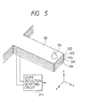
- Fig. 5 is a constitutional view of an integrated piezoelectric unimorph cantilever deflection sensor in the embodiment of the present invention.
- Fig. 1 show a first example of a recording/reproducing device.
- a plurality of conductive probe electrodes 104 supported by a plurality of cantilevers 101 comprising elastic members are disposed in the vicinity of a recording medium 107 so as to face to the medium 107.
- the multi-cantilevers 101 having the probe electrodes 104 which can be used herein can be formed as follows:
- An SiO 2 film having a thickness of 0.3 ⁇ m is produced on the surface of an Si substrate by thermal oxidation, and a multi-cantilever shape having a length of 100 ⁇ m and a width of 20 ⁇ m is then patterned thereon.
- an electric signal wiring pattern to probe electrodes is formed thereon, followed by anisotropic etching from the back surface of the substrate with a KOH solution to form the desired multi-cantilevers.
- probe electrodes having a height of 5 ⁇ m are disposed at the tips of the cantilevers in accordance with an electron beam deposition method using carbon or the like.
- the elastic constant to the deflection of each tip of the thus prepared multi-cantilevers is about 0.01 N/m.
- the unevenness of the heights of the probe electrodes on the basis of a multi-cantilever supporting member 102 is about 1 pm. Furthermore, the undulation of the recording medium surface is required to be about 1 ⁇ m or less.
- the recording medium 107 When the recording medium 107 is brought close to the plurality of probe electrodes 104 by a lengthwise driving element 108, the recording medium 107 applies a force to the nearest probe electrode, next the second nearest probe electrode, ..., and finally the farthest probe electrode of the plurality of probe electrodes 104.
- the probe electrode to which the force is applied by the medium and the strength of the applied force can be determined by detecting the deflection of the respective cantilevers (a manner for detecting the deflection of the cantilevers will be described hereinafter).
- the cantilever which is the elastic member for supporting the probe electrode is deflected. This deflection is directly proportional to the strength of the functional force.
- the strength of the force generated between the respective probe electrodes and the recording medium can be uniformized in the certain range and can be decreased so as to be in the range.
- the above-mentioned method can prevent the force of a threshold value or more of the breakage from being applied thereto, so that the recording medium and the probe electrodes can be protected from the breakage during recording and reproducing.
- a recording process will be described which is carried out by the probe electrodes 104 brought close to the recording medium 107 in the above-mentioned way.
- a horizontal position control signal is applied from a position control circuit 109 to a horizontal driving element 110, and the tip of the probe electrode 104 is moved to a desired position on the recording medium 107 at which recording should be made.
- a recording voltage signal from a voltage application circuit 111 for recording is applied to the probe electrode 104 selected by a switching circuit 112.
- the recording medium there can be used one such as to bring about a local shape change by the local application of voltage, electric field, or current.
- Examples of the recording medium include thin films of metals and metallic compounds, and typical examples include Au, Al, a Rh-Zr alloy mentioned in Appl. Phys. Lett. 51 , 244(1987) (Staufer et al.), a Te-Ti alloy, a Te-Se alloy, and Te-C, H type materials, and semiconductor thin films such as amorphous silicon and the like.
- examples of the material of the probe electrodes include tungsten, Pt-Ir and Pt.
- an etching process which comprises applying a voltage pulse onto the graphite surface, as shown in Appl. Phys. Lett. 55 , 1727 (1989) [Albrecht et al.].
- a light beam from a laser 114 is collected by a lens 115, and then allowed to fall upon a rotating polygon mirror 116.
- the rotational speed of the polygon mirror 116 is controlled by a rotational speed control circuit 117, and as the polygon mirror 116 is rotated, the reflected beam of the above-mentioned incident light beam scans the back surface of each of the plural cantilevers 101.
- the mirror surface of the polygon mirror 116 is inclined from the direction vertical with reference to the paper surface of Fig. 1, not only the cantilevers arranged in a horizontal direction on the paper surface of Fig.
- the cantilevers arranged in the vertical direction can be scanned.
- the position of the reflected light beam from the back surface of the cantilever is detected by a position detecting element 118.
- the length of the cantilever is represented by l and the distance between the back surface of the cantilever and the position detecting element is represented by L, and if the tip of the cantilever is deflected as much as ⁇ z, the position of the light spot of the reflected light beam from the back surface of the cantilever on the position detecting element 118 deviates as much as a distance of 2L l ⁇ z .
- the deflection (displacement) of the tip of each cantilever can be determined by detecting the deviated position of the light spot on the basis of the signal from the position detecting element 118 by a position detecting signal processing circuit 119.
- the scanning can be carried out with the light beam by the polygon mirror 116, and the deflection ⁇ z of the tip of each of the plural cantilevers 101 can be detected on the basis of the signal from the rotational speed control circuit 117 by time sharing.
- the surface of the recording medium 107 is two-dimensionally scanned by the plurality of probe electrodes 104, and when the probe electrode reaches a recording position, its local shape change leads to the change of the force which the probe electrode 104 receives from the recording medium 107, to change the deflection of the cantilever 101 supporting the probe electrode 104.
- This change of the deflection is successively detected on the plurality of cantilevers 101 by time sharing, whereby recorded bits are detected, i.e., they are reproduced.
- Fig. 2 shows a second recording/reproducing device.
- the arrangement of the multi-cantilevers 101, the approach way of the recording medium 107 to the plurality of probe electrodes 104, the recording way and the recording medium are the same as in Example 1.
- the distinctive features of the present example reside in a deflection detecting manner (i.e., reproduction) of the multi-cantilevers 101 and a constitution of the detection means. They will be described.
- An optically integrated deflection sensor 208 for detecting the deflection of each lever is integrally attached to the back surface of the multi-cantilevers 101.
- the optically integrated deflection sensor 208 is mainly composed of a semiconductor laser 209, an optical waveguide 216, a grating coupler 210 which is an optical path modulating element, and a photodiode 213, and the deflection of each cantilever 101 is detected on the basis of an output of the corresponding photodiode 213 by a lever deflection detecting circuit 217. Since the deflection detecting system is compactly integrated with the cantilevers, the positioning of the respective cantilevers to the deflection detecting system is not necessary any more, and operating efficiency can be improved. In addition, the whole of the apparatus can be miniaturized, and the influence of an outer turbulence can be inhibited. In consequence, the detection resolution can be improved, and the reliability of the recording/ reproducing apparatus can be also heightened.
- a semiconductor laser 209 attached to one edge of an SiO 2 302/Si substrate 303 provided on the surface thereof with the thin film optical waveguide 216 is driven by a semiconductor laser driving circuit 313 to introduce the laser light into the optical waveguide 216.
- the introduced laser light is collimated by a Fresnel lens 305 and then reflected by a reflecting mirror 306 to fall upon the grating coupler 210.
- a part of the light is taken out from the optical waveguide on the grating coupler 210 as shown by A, reflected on the back surface of the cantilever 101, returned to the optical waveguide on a grating coupler 210', and then synthesized with a light B straight delivered through the optical waveguide.
- the thus synthesized light C is reflected on a reflecting mirror 306', and then detected by the photodiode 213.
- the probe electrode 104 formed on the cantilever 101 detects the force generated between the probe electrode 104 and the recording medium, and the tip of the cantilever 101 is deflected in the direction of z in the drawing.
- this light intensity change permits determining the deflection ⁇ z of the tip of the cantilever 101 in the z direction.
- This light intensity change signal is amplified by an amplifying circuit 314 to obtain a z-direction deflection signal.
- a PIN photodiode 213 is formed on the Si substrate 303 by a usual silicon process, and an Si 3 N 4 protective film having a thickness of 0.1 ⁇ m is then formed thereon by an LPCVD method.
- an SiO 2 film 302 having a thickness of 2.5 ⁇ m is formed on another opening by thermal oxidation, and the Si 3 N 4 film is then removed by plasma etching.
- a Fresnel lens 305 and the grating couplers 210 and 210' are prepared in the waveguide by the utilization of a refractive index change by ion exchange or ion injection.
- another Si substrate 316 having an SiO 2 film 315 thereon is patterned into a cantilever shape, and after the formation of an A1 wiring 317 and the probe electrode 104, a chip having the multi-cantilevers formed by anisotropic etching is mounted on the glass thin film waveguide by anodic bonding. After cleavage and polishing, a metal such as A1 is vapor deposited on edges of the chip to provide the reflecting mirrors 306 and 306', and the semiconductor laser 209 is attached to the another edge of the chip.
- Fig. 4 is a drawing showing an embodiment of the present invention.
- the arrangement of the multi-cantilevers, the approach way of the recording medium 107 to the plurality of probe electrodes 104, the recording way and the recording medium are the same as in Example 1.
- the distinctive features of the present example reside in a deflection detecting manner (i.e., reproduction) of the multi-cantilevers 101 and the constitution of the detection means. They will be described.
- Deflection sensors 408 each comprising metallic electrodes and a piezoelectric layer sandwiched therebetween are integrally mounted on the back surfaces of the respective cantilevers 101.
- Each deflection sensor 408 has a piezoelectric unimorph structure associated with a constitutional member of the cantilever, as shown in Fig. 5.
- the probe electrode 104 detects the force generated between the probe electrode 104 and the recording medium 107, so that the tip of the cantilever 101 deflects in the z direction in the drawing.
- the piezoelectric layer 505 strains, with the result that a potential difference takes place between the Au electrodes 504 and 506.
- the cantilever 101 has a length of 100 ⁇ m and a width of 20 ⁇ m and when the Au electrode 502, an SiO 2 layer 503, the Au electrode 504, the piezoelectric layer (ZnO) 505 and the Au electrode 506 are 0.1 pm, 1 ⁇ m, 0.1 ⁇ m, 1 ⁇ m and 0.1 ⁇ m thick, respectively, and if the deflection ⁇ z of the cantilever is 1 nm, a potential difference of about 1 mV is generated. Therefore, the deflection of the cantilever tip can be determined by detecting this potential difference by the lever deflection detecting circuit 217.
- the preparation method of such piezoelectric unimorph cantilevers While the Si substrate is successively patterned into cantilever shapes thereon, the Au thin film (thickness 0.1 ⁇ m) is formed by a vapor deposition method and the ZnO thin film (thickness 1 ⁇ m) and the SiO 2 thin film (thickness 1 ⁇ m) are formed by a sputtering method so as to be alternately laminated. Afterward, a conductive material is vapor deposited by an electron beam deposition method to prepare probe electrodes. In the final step, an isotropic etching is carried out by the use of KOH from the back surface of the substrate to form the desired cantilevers.
- an information processor having a high reliability can be achieved by a micromachine technology into each of the cantilevers, whereby the deflections of plural cantilevers can be detected without enlarging the constitution of the whole apparatus, and the reproduction time can be shortened.
Abstract
Description
Claims (6)
- An apparatus for reproducing information recorded on a recording medium comprising:a plurality of probes (104) arranged to face the recording medium (107);a plurality of elastic members (101) each arranged to support a respective one of said plurality of probes (104), each elastic member (101) being susceptible to deflection by a functional force generated between the associated probe (104) and said recording medium (107);a plurality of detecting means (408) each effective to detect the deflection of a respective elastic member (101); anda signal forming means (217) for forming a reproduction signal representing the recorded information on the basis of an output signal from said plurality of detecting means (408),said apparatus being characterised in that a respective one of said detecting means (408) is integrated into each elastic member (101); and in thateach said detecting means (408) comprises a pair of electrodes (504,506) with piezoelectric material (505) sandwiched therebetween, such that the deflection of the corresponding elastic member (101) may be measured by the potential difference between said pair of electrodes (504,506) generated by the strain produced in said piezoelectric material (505) by the deflection of the corresponding elastic member (101).
- An apparatus according to claim 1, wherein said detecting means (408) has a piezoelectric unimorph structure.
- An apparatus according to claim 1 or claim 2, further comprising means (111) for applying a voltage between the recording medium (107) and the probes (104).
- An apparatus according to any one of the preceding claims, wherein each elastic member (101) is a cantilever.
- An apparatus according to any one of the preceding claims, wherein the electrodes (504,506) comprise Au and the piezoelectric material (505) sandwiched therebetween comprises ZnO.
- An apparatus according to any one of the preceding claims including means (111) for recording information on the recording medium (107) using at least one of said plurality of probes (104).
Applications Claiming Priority (2)
| Application Number | Priority Date | Filing Date | Title |
|---|---|---|---|
| JP116545/91 | 1991-04-22 | ||
| JP3116545A JP3000492B2 (en) | 1991-04-22 | 1991-04-22 | Information processing device |
Publications (3)
| Publication Number | Publication Date |
|---|---|
| EP0510895A2 EP0510895A2 (en) | 1992-10-28 |
| EP0510895A3 EP0510895A3 (en) | 1994-06-01 |
| EP0510895B1 true EP0510895B1 (en) | 1998-10-28 |
Family
ID=14689770
Family Applications (1)
| Application Number | Title | Priority Date | Filing Date |
|---|---|---|---|
| EP92303508A Expired - Lifetime EP0510895B1 (en) | 1991-04-22 | 1992-04-21 | Information processor |
Country Status (6)
| Country | Link |
|---|---|
| US (1) | US5260926A (en) |
| EP (1) | EP0510895B1 (en) |
| JP (1) | JP3000492B2 (en) |
| AT (1) | ATE172810T1 (en) |
| CA (1) | CA2066343C (en) |
| DE (1) | DE69227397T2 (en) |
Families Citing this family (33)
| Publication number | Priority date | Publication date | Assignee | Title |
|---|---|---|---|---|
| JPH041949A (en) * | 1990-04-18 | 1992-01-07 | Canon Inc | Information input and/or output device |
| JPH041948A (en) * | 1990-04-18 | 1992-01-07 | Canon Inc | Information recorder, information reproducer and their applied information recording and reproducing device |
| JPH05282717A (en) * | 1992-03-31 | 1993-10-29 | Canon Inc | Manufacture of recording medium, and recording medium and information processor |
| JP2895694B2 (en) * | 1992-12-08 | 1999-05-24 | シャープ株式会社 | Information recording / reproducing slider, method of manufacturing information recording / reproducing slider, and information recording / reproducing apparatus |
| JP3384009B2 (en) * | 1992-12-25 | 2003-03-10 | キヤノン株式会社 | Digital television receiver |
| DE4310349C2 (en) * | 1993-03-30 | 2000-11-16 | Inst Mikrotechnik Mainz Gmbh | Sensor head and method for its production |
| JP3162883B2 (en) * | 1993-09-29 | 2001-05-08 | キヤノン株式会社 | Information recording / reproducing device |
| US5633455A (en) * | 1993-10-05 | 1997-05-27 | Board Of Trustees Of The Leland Stanford, Jr. University | Method of detecting particles of semiconductor wafers |
| US20020053734A1 (en) | 1993-11-16 | 2002-05-09 | Formfactor, Inc. | Probe card assembly and kit, and methods of making same |
| US5453616A (en) * | 1994-10-18 | 1995-09-26 | Seiko Instruments, Inc. | Probe microscope having error correction piezoelectric scanner |
| US20100065963A1 (en) | 1995-05-26 | 2010-03-18 | Formfactor, Inc. | Method of wirebonding that utilizes a gas flow within a capillary from which a wire is played out |
| US5874668A (en) * | 1995-10-24 | 1999-02-23 | Arch Development Corporation | Atomic force microscope for biological specimens |
| JPH09196933A (en) * | 1996-01-19 | 1997-07-31 | Canon Inc | Probe, its production, probe unit, and data recording and reproducing apparatus using the same |
| US8033838B2 (en) | 1996-02-21 | 2011-10-11 | Formfactor, Inc. | Microelectronic contact structure |
| JPH10246730A (en) * | 1997-03-04 | 1998-09-14 | Canon Inc | Probe and its production, and information-processing apparatus with the probe |
| US6139759A (en) | 1997-07-08 | 2000-10-31 | International Business Machines Corporation | Method of manufacturing silicided silicon microtips for scanning probe microscopy |
| US7304486B2 (en) * | 1998-07-08 | 2007-12-04 | Capres A/S | Nano-drive for high resolution positioning and for positioning of a multi-point probe |
| US6708556B1 (en) * | 1999-06-05 | 2004-03-23 | Daewoo Electronics Corporation | Atomic force microscope and driving method therefor |
| US6525307B1 (en) * | 1999-09-16 | 2003-02-25 | Ut-Battelle, Llc | Integrated optical interrogation of micro-structures |
| US7262611B2 (en) | 2000-03-17 | 2007-08-28 | Formfactor, Inc. | Apparatuses and methods for planarizing a semiconductor contactor |
| US6729019B2 (en) | 2001-07-11 | 2004-05-04 | Formfactor, Inc. | Method of manufacturing a probe card |
| EP1575058A1 (en) * | 2004-03-08 | 2005-09-14 | Consejo Superior De Investigaciones Cientificas | System and method for detecting the displacement of a plurality of micro- and nanomechanical elements, such as micro-cantilevers |
| US7571638B1 (en) * | 2005-05-10 | 2009-08-11 | Kley Victor B | Tool tips with scanning probe microscopy and/or atomic force microscopy applications |
| US9423693B1 (en) | 2005-05-10 | 2016-08-23 | Victor B. Kley | In-plane scanning probe microscopy tips and tools for wafers and substrates with diverse designs on one wafer or substrate |
| US7136215B1 (en) * | 2005-05-18 | 2006-11-14 | Avago Technologies Fiber Ip (Singapore) Pte. Ltd. | Piezoelectrically-activated cantilevered spatial light modulator |
| US7622780B2 (en) * | 2006-12-21 | 2009-11-24 | Intel Corporation | Seek-scan probe (SSP) including see-saw scan probe with redundant tip |
| JP4946763B2 (en) * | 2007-10-01 | 2012-06-06 | ブラザー工業株式会社 | Bending detector |
| JP2010156682A (en) * | 2008-12-04 | 2010-07-15 | Kinki Univ | Potential measuring instrument for live object and measurement method using the same |
| WO2010085768A1 (en) * | 2009-01-26 | 2010-07-29 | Nanoink,Inc. | Large area, homogeneous array fabbrication including leveling with use of bright spots |
| US9835591B2 (en) | 2011-02-25 | 2017-12-05 | Panorama Synergy Ltd | Optical cantilever based analysis |
| US20130205455A1 (en) * | 2012-02-07 | 2013-08-08 | University Of Western Australia | System and method of performing atomic force measurements |
| US9057706B2 (en) | 2011-02-25 | 2015-06-16 | University Of Western Australia | Optical cantilever based analyte detection |
| US9778572B1 (en) | 2013-03-15 | 2017-10-03 | Victor B. Kley | In-plane scanning probe microscopy tips and tools for wafers and substrates with diverse designs on one wafer or substrate |
Family Cites Families (14)
| Publication number | Priority date | Publication date | Assignee | Title |
|---|---|---|---|---|
| US3609002A (en) * | 1969-12-30 | 1971-09-28 | Bell Telephone Labor Inc | Multiple element optical memory structures using fine grain ferroelectric ceramics |
| JPS60143462A (en) * | 1983-12-29 | 1985-07-29 | Fuji Photo Film Co Ltd | Method and device for reproducing magnetic recording information |
| DE3509710C2 (en) * | 1984-04-13 | 1996-03-28 | Xerox Corp | Electrostatic voltmeter |
| JPS62112242A (en) * | 1985-11-11 | 1987-05-23 | Hitachi Ltd | Multi-reproduction light pick-up |
| JP2756254B2 (en) * | 1988-03-25 | 1998-05-25 | キヤノン株式会社 | Recording device and playback device |
| JPH02187944A (en) * | 1989-01-13 | 1990-07-24 | Sharp Corp | Reproducing device |
| GB8910566D0 (en) * | 1989-05-08 | 1989-06-21 | Amersham Int Plc | Imaging apparatus and method |
| JP2628790B2 (en) * | 1989-06-23 | 1997-07-09 | ザ ボード オブ トラスティーズ オブ ザ リーランド スタンフォード ジュニア ユニバーシティ | Method and apparatus for storing digital information in the form of stored charges |
| DE68903951T2 (en) * | 1989-08-16 | 1993-07-08 | Ibm | METHOD FOR PRODUCING MICROMECHANICAL PROBE FOR AFM / STM PROFILOMETRY AND MICROMECHANICAL PROBE HEAD. |
| US5144128A (en) * | 1990-02-05 | 1992-09-01 | Hitachi, Ltd. | Surface microscope and surface microscopy |
| US5065103A (en) * | 1990-03-27 | 1991-11-12 | International Business Machines Corporation | Scanning capacitance - voltage microscopy |
| US5187367A (en) * | 1990-08-14 | 1993-02-16 | Canon Kabushiki Kaisha | Cantilever type probe, scanning tunneling microscope and information processing device equipped with said probe |
| JPH04115103A (en) * | 1990-09-05 | 1992-04-16 | Canon Inc | Cantilever type probe, scanning type tunnel microscope using the probe, precise positioning apparatus and information processing apparatus |
| US5166520A (en) * | 1991-05-13 | 1992-11-24 | The Regents Of The University Of California | Universal, microfabricated probe for scanning probe microscopes |
-
1991
- 1991-04-22 JP JP3116545A patent/JP3000492B2/en not_active Expired - Fee Related
-
1992
- 1992-04-16 CA CA002066343A patent/CA2066343C/en not_active Expired - Lifetime
- 1992-04-17 US US07/870,335 patent/US5260926A/en not_active Expired - Lifetime
- 1992-04-21 AT AT92303508T patent/ATE172810T1/en not_active IP Right Cessation
- 1992-04-21 EP EP92303508A patent/EP0510895B1/en not_active Expired - Lifetime
- 1992-04-21 DE DE69227397T patent/DE69227397T2/en not_active Expired - Fee Related
Also Published As
| Publication number | Publication date |
|---|---|
| DE69227397D1 (en) | 1998-12-03 |
| EP0510895A3 (en) | 1994-06-01 |
| ATE172810T1 (en) | 1998-11-15 |
| EP0510895A2 (en) | 1992-10-28 |
| CA2066343C (en) | 1995-10-03 |
| JPH04321955A (en) | 1992-11-11 |
| US5260926A (en) | 1993-11-09 |
| CA2066343A1 (en) | 1992-10-23 |
| DE69227397T2 (en) | 1999-04-29 |
| JP3000492B2 (en) | 2000-01-17 |
Similar Documents
| Publication | Publication Date | Title |
|---|---|---|
| EP0510895B1 (en) | Information processor | |
| EP0791803B1 (en) | Cantilever unit and atomic force microscope, magnetic force microscope, reproducing apparatus and information processing apparatus using the cantilever unit | |
| US5247186A (en) | Integrated optical displacement sensor | |
| US5231286A (en) | Scanning probe microscope utilizing an optical element in a waveguide for dividing the center part of the laser beam perpendicular to the waveguide | |
| EP1061510B1 (en) | Near-field optical head and production method thereof | |
| US5908981A (en) | Interdigital deflection sensor for microcantilevers | |
| US5412641A (en) | Information recording/reproducing apparatus for recording/reproducing information with probes | |
| US5506829A (en) | Cantilever probe and apparatus using the same | |
| US7182876B2 (en) | Cantilever microstructure and fabrication method thereof | |
| JPH09269329A (en) | Method of manufacturing probe having minute opening, composite device of scanning proximity field optical microscope and scanning tunnel microscope using the probe and recorder/reproducer using the probe | |
| US5717680A (en) | Information processing apparatus with mechanism for adjusting interval between substrate for supporting a plurality of probes and recording medium | |
| EP0452851B1 (en) | Information recording/reproducing apparatus | |
| JP3069923B2 (en) | Cantilever probe, atomic force microscope, information recording / reproducing device | |
| JPH0721968A (en) | Cantilever type displacement element, cantilever type probe using the displacement element, and scanning type probe microscope and data processer using the probe | |
| EP0722077B1 (en) | Information processing apparatus effecting probe position control with electrostatic forces | |
| JP3203433B2 (en) | Displacement element, detection element using the same, scanning tunnel microscope using the detection element, information processing apparatus | |
| Egawa et al. | High‐speed scanning by dual feedback control in SNOM/AFM | |
| JPH085642A (en) | Integrated multifunction spm sensor | |
| CA2031733C (en) | Method for forming probe and apparatus therefor | |
| JPH04131710A (en) | Scanning type probe microscope | |
| JPH0875761A (en) | Scanning probe microscope as well as processing apparatus using the microscope and data-processing apparatus | |
| JPH0571951A (en) | Interatomic power microscope and information processor | |
| JP3234952B2 (en) | Probe unit, scanning tunneling microscope and information processing apparatus using the same | |
| JPH08146015A (en) | Cantilever of scanning type probe microscope | |
| JPH117667A (en) | Device and method for recording/reproducing |
Legal Events
| Date | Code | Title | Description |
|---|---|---|---|
| PUAI | Public reference made under article 153(3) epc to a published international application that has entered the european phase |
Free format text: ORIGINAL CODE: 0009012 |
|
| AK | Designated contracting states |
Kind code of ref document: A2 Designated state(s): AT BE CH DE DK ES FR GB GR IT LI LU NL PT SE |
|
| PUAL | Search report despatched |
Free format text: ORIGINAL CODE: 0009013 |
|
| AK | Designated contracting states |
Kind code of ref document: A3 Designated state(s): AT BE CH DE DK ES FR GB GR IT LI LU NL PT SE |
|
| 17P | Request for examination filed |
Effective date: 19941013 |
|
| 17Q | First examination report despatched |
Effective date: 19960710 |
|
| GRAG | Despatch of communication of intention to grant |
Free format text: ORIGINAL CODE: EPIDOS AGRA |
|
| GRAG | Despatch of communication of intention to grant |
Free format text: ORIGINAL CODE: EPIDOS AGRA |
|
| GRAH | Despatch of communication of intention to grant a patent |
Free format text: ORIGINAL CODE: EPIDOS IGRA |
|
| GRAH | Despatch of communication of intention to grant a patent |
Free format text: ORIGINAL CODE: EPIDOS IGRA |
|
| GRAA | (expected) grant |
Free format text: ORIGINAL CODE: 0009210 |
|
| AK | Designated contracting states |
Kind code of ref document: B1 Designated state(s): AT BE CH DE DK ES FR GB GR IT LI LU NL PT SE |
|
| PG25 | Lapsed in a contracting state [announced via postgrant information from national office to epo] |
Ref country code: CH Free format text: LAPSE BECAUSE OF FAILURE TO SUBMIT A TRANSLATION OF THE DESCRIPTION OR TO PAY THE FEE WITHIN THE PRESCRIBED TIME-LIMIT Effective date: 19981028 Ref country code: LI Free format text: LAPSE BECAUSE OF FAILURE TO SUBMIT A TRANSLATION OF THE DESCRIPTION OR TO PAY THE FEE WITHIN THE PRESCRIBED TIME-LIMIT Effective date: 19981028 Ref country code: GR Free format text: LAPSE BECAUSE OF NON-PAYMENT OF DUE FEES Effective date: 19981028 Ref country code: ES Free format text: THE PATENT HAS BEEN ANNULLED BY A DECISION OF A NATIONAL AUTHORITY Effective date: 19981028 Ref country code: NL Free format text: LAPSE BECAUSE OF FAILURE TO SUBMIT A TRANSLATION OF THE DESCRIPTION OR TO PAY THE FEE WITHIN THE PRESCRIBED TIME-LIMIT Effective date: 19981028 Ref country code: BE Free format text: LAPSE BECAUSE OF FAILURE TO SUBMIT A TRANSLATION OF THE DESCRIPTION OR TO PAY THE FEE WITHIN THE PRESCRIBED TIME-LIMIT Effective date: 19981028 Ref country code: AT Free format text: LAPSE BECAUSE OF FAILURE TO SUBMIT A TRANSLATION OF THE DESCRIPTION OR TO PAY THE FEE WITHIN THE PRESCRIBED TIME-LIMIT Effective date: 19981028 |
|
| REF | Corresponds to: |
Ref document number: 172810 Country of ref document: AT Date of ref document: 19981115 Kind code of ref document: T |
|
| REG | Reference to a national code |
Ref country code: CH Ref legal event code: EP |
|
| REF | Corresponds to: |
Ref document number: 69227397 Country of ref document: DE Date of ref document: 19981203 |
|
| ET | Fr: translation filed | ||
| PG25 | Lapsed in a contracting state [announced via postgrant information from national office to epo] |
Ref country code: SE Free format text: LAPSE BECAUSE OF FAILURE TO SUBMIT A TRANSLATION OF THE DESCRIPTION OR TO PAY THE FEE WITHIN THE PRESCRIBED TIME-LIMIT Effective date: 19990128 Ref country code: PT Free format text: LAPSE BECAUSE OF FAILURE TO SUBMIT A TRANSLATION OF THE DESCRIPTION OR TO PAY THE FEE WITHIN THE PRESCRIBED TIME-LIMIT Effective date: 19990128 Ref country code: DK Free format text: LAPSE BECAUSE OF FAILURE TO SUBMIT A TRANSLATION OF THE DESCRIPTION OR TO PAY THE FEE WITHIN THE PRESCRIBED TIME-LIMIT Effective date: 19990128 |
|
| NLV1 | Nl: lapsed or annulled due to failure to fulfill the requirements of art. 29p and 29m of the patents act | ||
| PG25 | Lapsed in a contracting state [announced via postgrant information from national office to epo] |
Ref country code: LU Free format text: LAPSE BECAUSE OF NON-PAYMENT OF DUE FEES Effective date: 19990421 |
|
| REG | Reference to a national code |
Ref country code: CH Ref legal event code: PL |
|
| PLBE | No opposition filed within time limit |
Free format text: ORIGINAL CODE: 0009261 |
|
| STAA | Information on the status of an ep patent application or granted ep patent |
Free format text: STATUS: NO OPPOSITION FILED WITHIN TIME LIMIT |
|
| 26N | No opposition filed | ||
| REG | Reference to a national code |
Ref country code: GB Ref legal event code: IF02 |
|
| PGFP | Annual fee paid to national office [announced via postgrant information from national office to epo] |
Ref country code: DE Payment date: 20090430 Year of fee payment: 18 Ref country code: IT Payment date: 20090417 Year of fee payment: 18 Ref country code: FR Payment date: 20090424 Year of fee payment: 18 |
|
| PGFP | Annual fee paid to national office [announced via postgrant information from national office to epo] |
Ref country code: GB Payment date: 20090428 Year of fee payment: 18 |
|
| GBPC | Gb: european patent ceased through non-payment of renewal fee |
Effective date: 20100421 |
|
| REG | Reference to a national code |
Ref country code: FR Ref legal event code: ST Effective date: 20101230 |
|
| PG25 | Lapsed in a contracting state [announced via postgrant information from national office to epo] |
Ref country code: FR Free format text: LAPSE BECAUSE OF NON-PAYMENT OF DUE FEES Effective date: 20100430 |
|
| PG25 | Lapsed in a contracting state [announced via postgrant information from national office to epo] |
Ref country code: DE Free format text: LAPSE BECAUSE OF NON-PAYMENT OF DUE FEES Effective date: 20101103 |
|
| PG25 | Lapsed in a contracting state [announced via postgrant information from national office to epo] |
Ref country code: IT Free format text: LAPSE BECAUSE OF NON-PAYMENT OF DUE FEES Effective date: 20100421 Ref country code: GB Free format text: LAPSE BECAUSE OF NON-PAYMENT OF DUE FEES Effective date: 20100421 |