EP0510482A1 - Procédé et dispositif d'adressage de périphériques pour le partage d'un canal de transmission de données entre les périphériques - Google Patents
Procédé et dispositif d'adressage de périphériques pour le partage d'un canal de transmission de données entre les périphériques Download PDFInfo
- Publication number
- EP0510482A1 EP0510482A1 EP92106371A EP92106371A EP0510482A1 EP 0510482 A1 EP0510482 A1 EP 0510482A1 EP 92106371 A EP92106371 A EP 92106371A EP 92106371 A EP92106371 A EP 92106371A EP 0510482 A1 EP0510482 A1 EP 0510482A1
- Authority
- EP
- European Patent Office
- Prior art keywords
- addressing
- peripherals
- signal
- management unit
- interface
- Prior art date
- Legal status (The legal status is an assumption and is not a legal conclusion. Google has not performed a legal analysis and makes no representation as to the accuracy of the status listed.)
- Withdrawn
Links
Images

Classifications
-
- G—PHYSICS
- G06—COMPUTING; CALCULATING OR COUNTING
- G06F—ELECTRIC DIGITAL DATA PROCESSING
- G06F12/00—Accessing, addressing or allocating within memory systems or architectures
- G06F12/02—Addressing or allocation; Relocation
- G06F12/06—Addressing a physical block of locations, e.g. base addressing, module addressing, memory dedication
- G06F12/0646—Configuration or reconfiguration
- G06F12/0653—Configuration or reconfiguration with centralised address assignment
- G06F12/0661—Configuration or reconfiguration with centralised address assignment and decentralised selection
Definitions
- the field of the invention is that of methods and devices for addressing peripherals. More specifically, the present invention relates to a time-division multiplexed addressing method and device for sharing a transmission channel between a certain number of peripherals, particularly applicable in the field of telephone and / or data communications.
- addressing of a peripheral by a management unit for example by a microprocessor, can be carried out in three different ways.
- the first, most commonly used, is to distribute an address bus on each device.
- the management unit sends on this bus the address of the peripheral which will be affected by the data circulating on the data bus.
- Each device then locally has its own address decoding means, typically logic gates, which determine whether the corresponding device is addressed or not.
- This addressing structure is costly in terms of links, in decoding means, and has a large bulk due to the size of the bus and the location occupied by the decoding means. The possibilities of extending such addressing are further reduced, since it is not easy to add a large number of peripherals to those already existing, for reasons of current load of the bus. Finally, it is not possible to address with such a structure simultaneously more than one device. For this, it is necessary to carry out successive addressing, costly in time.
- the second addressing system is to provide each device with an address wire.
- the addressing of a peripheral is then carried out by modifying the logical state of the line, for example by generating a high logic level on the line. Typically, this logic level corresponds to a "Chip Select".
- this structure also requires a large number of wires, this number increasing with the number of peripherals.
- the third addressing system consists in removing the address bus and in addressing a device by the data bus, before sending data.
- This structure corresponds to that of an Ethernet type bus where the messages transmitted are in the form of packets.
- Each packet comprises, in the transmission order, a header indicating in particular the destination of the data, the data to be transmitted and an indication of end of packet with possibly a cyclic redundancy code (CRC).
- CRC cyclic redundancy code
- the present invention aims in particular to overcome these drawbacks.
- one of the objectives of the present invention is to provide a device and a method for addressing peripherals which does not require protocol management on the transmission channel and which completely frees the transmission channel for the data.
- Another object of the present invention is to provide such a device which has only a reduced structure and thus facilitates wiring.
- An additional objective of the invention is to allow simultaneous addressing of several peripherals.
- the device could thus operate in multi-addressing mode.
- a complementary objective of the invention is to achieve, using such a method and device, communication between a PABX and PABX-telephone terminal interface cards, which can be adapted to already existing automatic branch exchange devices without calling into question the original items.
- a device addressing method of the type consisting in generating an addressing signal intended to address at least one device, the addressing signal being generated by a management unit controlling the peripherals, said method consisting in assigning, during a programming phase, a separate number to each interface corresponding to a determined rank of time interval composing said addressing signal, and in addressing, during an addressing phase, the peripherals whose numbers correspond respectively to activated time slots of the addressing signal.
- the peripherals are validated for the duration of a frame following the frame during which they were addressed.
- the invention also relates to an addressing device implementing such a method, the device comprising a single address wire connected between the management unit and each of the peripherals, the single conductive wire carrying the addressing signal.
- the peripherals are interfaces between a data transmission channel common to the interfaces and terminals.
- the terminals are telephone and / or telematic terminals.
- each of the peripherals comprises means for comparing a reference clock signal with the address signal, the comparison means generating a validation signal when the address signal comprises an activated time interval corresponding to the number program.
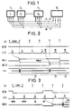
- Figure 1 is a block diagram of the device according to the present invention.
- the device comprises a management unit 10 communicating with peripherals 11, 12, 13 respectively called I1, I2, I n .
- the number n of peripherals has been deliberately limited to three in this figure for reasons of clarity, but the number n is in theory not limited.
- the management unit 10 is the single master, while the peripherals I1, I2 I n are the slaves.
- Each peripheral is connected to the management unit 10 by four links 14, 15, 16, 17.
- Link 14 is a bidirectional data transmission channel.
- the peripherals I1, I2, and I n are peripherals between the transmission channel 14 and telephone and / or telematic stations not shown.
- the device of Figure 1 is for example located in a private branch exchange of the PABX type.
- the link 14 is then organized in time intervals.
- the link 15 is constituted, according to the invention, by a single wire intended to convey addressing information, as will be described below with reference to FIG. 2.
- the link 16 is also formed by a single wire carrying a read / write signal.
- the link 17 carries a bit clock signal and a frame clock signal.
- the bit clock has a frequency of 2.048 MHz and the frame clock has a frequency of 8 KHz.
- This embodiment corresponds to addressing using a MIC type frame as will be explained below.
- Data exchanges between the management unit 10 and the interfaces I1, I2, I n are done from point to multipoint in the master to slave direction (from 1 to n recipients) without any protocol.
- FIG. 2 is a timing diagram illustrating a phase of writing from the management unit to one then two peripherals.
- This timing diagram includes the following signals: the signal SY is the frame clock signal also called frame synchronization signal. It has a frequency of 8 KHz and two synchronization signals are therefore separated by 125 ⁇ s.
- the RW signal is the read / write signal. In the case of FIG. 2, this signal is in a writing phase.
- the signal S15 is an addressing signal conveyed on the addressing link 15 (FIG. 1).
- the signals VAL 4 and VAL 20 correspond respectively to the validation of the interfaces 4 and 20, as will be explained below.
- the signal S14 is a digital signal conveyed by the data transmission channel 14.
- each interface is programmed with a unique time slot number which makes it possible to generate a validation window when the management unit positions this same number on the signal addressing, during an addressing phase.
- Each addressing phase has, according to a preferred embodiment, a duration of 125 ⁇ s.
- This is subdivided, according to one embodiment, into 32 equal time intervals. By positioning each of these 32 time slots in the active or inactive state, it is possible to address between 0 and 32 interfaces at each addressing phase.
- the addressing signal S15 positions its fourth time interval in the active state. This positioning is for example achieved by setting to the state "1" the eight bits of the fourth time interval.
- the interface which was programmed during the initialization phase with the number 4 detects this active state and is ready to receive data. This interface is called I4.
- the signal VAL4 internal to the interface I4 is automatically activated for the duration of a frame.
- the management unit 10 then generates on the transmission channel 14 data intended for I4 (signal S14).
- the interface I4 is kept active for four successive frames, ie 500 ⁇ s.
- the interface I20 is also addressed by the management unit 10, that is to say that the twentieth time interval of the addressing signal S15 is activated.
- the interface I20 is then activated from the start of the fifth frame of the signal S15.
- the fifth addressing frame no longer has a fourth active time slot and the interface I4 is deactivated at the end of the fifth frame.
- the period 21 of the signal S14 is received by the interface I4, the period 22 by the interfaces I4 and I20 and period 23 via the I20 interface only.
- the method of the invention therefore makes it possible to address simultaneously and selectively as many interfaces as there are time intervals in a frame of the addressing signal.
- the addressing performed has the particular advantage of not including any protocol. This addressing makes it possible to write in an interface but also to read data coming from the interfaces.
- FIG. 3 is a timing diagram illustrating a reading phase of the data management unit originating from a peripheral.
- Reading the data coming from an interface supposes the implementation of a protocol intended to detect the interface wanting to transmit. This protocol consists in cyclically interrogating the interfaces to recognize the one which wishes to send a message to the management unit 10.
- the direction of data propagation is represented by the variable SENS.
- SENS The direction of data propagation is represented by the variable SENS.
- the transmission has instead of an interface to the management unit 10 while a low state signifies a data transmission from the management unit 10 to an interface.
- the management unit 10 switches to read mode at the start of a frame of the signal SY and successively addresses the interfaces 1 to n.
- Addressing consists in validating the time interval of a frame of the addressing signal, the successive time intervals of successive frames being validated.
- the interface I1 transmits a REST code signaling to the management unit 10 that it has no message to send.
- the management unit addresses, by activating the second time interval of a second frame, the interface I2.
- the latter also sends a REPOS code via the transmission channel 14 to the management unit 10.
- the offsets of a frame between the addressing of an interface and its validation are not shown for reasons of ease of understanding. .
- the management unit 10 then interrupts the scanning of the interfaces and goes into write mode at the start of the fourth frame. It addresses the I3 interface and sends it an AE code meaning Authorization to Send.
- the management unit 10 then switches to read mode and the AE code is read by the interface I3 (fifth frame). Since the interface I3 is always addressed, the latter then sends its message M3 to the management unit 10.
- FIG. 4 is a block diagram of an embodiment of the management unit.
- the management unit 10 comprises a microprocessor 40, a transceiver 41, a timepiece 42, a counter-comparator 43 and synchronization means 44.
- the microprocessor 40 dialogues with the transceiver 41 and the counter-comparator 43 using an internal bus 45. It is controlled by the clock 42 which makes it possible to obtain the bit clock signal H and the frame clock SY. H and SY allow the management unit 10 to control the interfaces In synchronously.
- the microprocessor 40 defines the interface In to be selected and transmits the number of the interface to the counter-comparator 43 which generates the address signal Sn.
- the counter-comparator 43 divides the frame signal of duration 125 ⁇ s into 32 equal time intervals, each time interval also being divided into 8 zones.
- the 8 zones of a time interval are put in the logical state "1" for the addressing of an interface.
- a comparison between H, SY and the addressing signal Sn makes it possible to determine whether or not the interface is addressed.
- the synchronization means 44 generate, from an R / W signal coming from the microprocessor 40, the R / W read-write signal synchronized with the frame clock SY.
- the data present on the transmission channel 14 is routed to the microprocessor 40 by means of the transceiver 41 as a function of the R / W signal synchronized with SY.
- the management unit 10 manages the cyclic scanning of the interfaces In when data messages can come from the interfaces.
- FIG. 5 is a block diagram of an embodiment of a peripheral constituted by an interface between a transmission channel and a telephone and / or telematic station.
- Each interface In comprises a counter-comparator 50, a transceiver 51, a buffer 52 and a line interface 53.
- the interfaces In also include management means, not shown.
- the counter-comparator 50 compares the signals H, SY, and Sn and validates the transceiver 51, with a delay of a frame, if the time interval corresponding to the time slot number assigned to the interface is activated .
- the comparison carried out corresponds to a sampling of the addressing signal, the sampling being carried out when the time interval programmed is reached.
- the sampling carried out at the interface makes it possible to simply decode the addressing signal. It actually consists in examining a very precise time window corresponding to the number assigned to the interface.
- the transceiver 51 is validated by the signal VALn as long as the interface In is addressed, with an offset frame period (see FIG. 2).
- the transceiver 51 is controlled by the R / W signal synchronized with the frame clock SY.
- the data conveyed on the transmission channel 14 are directed towards the line interface 53 via the buffer 52.
- the line interface 53 can for example be connected to a telephone set 55 via a two-wire connection 54. Any other type of terminal is also suitable.
- the data can be routed from the terminal 55 to the management unit 10.
- the buffer 52 is used to store data to be transmitted from the management unit 10 to the terminal 55 or from the terminal 55 to the management unit 10. This buffer makes it possible to adapt the data rates.
- the number programmed in the interface is stored in storage means (not shown) cooperating with the counter-comparator 50 to allow sampling of the address signal during the time interval corresponding to this number.
- the programming of the interfaces can be carried out by software, for example at the initialization of the device, by means of a bus not shown of the Ethernet type.
- This programming can also be of the physical type, that is to say that each interface comprises switches of the DIL type making it possible to distinguish each of the interfaces.
- the means for memorizing the number assigned to each interface are therefore no longer necessary since it suffices to read the configuration. switches to find out the number of an interface.
- the device of the invention can therefore operate in writing and in reading. It is of course possible to keep only one direction of transmission of the management unit information to the interface. This embodiment has the advantage of requiring only receivers at the interface level and no communication protocol since the entire device operates synchronously. It is also possible to establish a bidirectional connection using an additional bus on which the write request protocol would be made.
- Another embodiment of the invention consists in managing the address link and the data bus to send data to a peripheral from the time interval following its addressing. An appreciable time saving is obtained, however involving a more complex management of the device.
- the data transmission channel is divided into a number of intervals multiple of that of the frame of the address signal.
- the transmissions carried out be synchronous with the addressing signal.
- the data transmission channel and the address signal are both divided into 32 time intervals (conventional MIC link) with a bit H clock of 2.048 MHz.
- the bit clock of the data transmission channel has a frequency twice that of the addressing signal.
- the present invention preferably applies to the management of communications between a PABX and telephone and / or telematic stations via interfaces of type In.
- the device of the invention is advantageously included in a PABX operating with MIC links.
- the clock 42 of the management unit 10 (FIG. 4) can then not be included in the management unit and come directly from the automatic exchange.
- This switch includes a central control unit which controls the CPUs 40 of each management unit dedicated to a specific application.
- the management unit 10 can for example be assigned to a imaging application.
- This embodiment makes it possible to integrate the device of the invention in already existing systems, at low cost and without calling into question the means already used.
- the invention can also be applied to the control of printers controllers, graphic controllers, etc.
- the transmitted data can be different depending on the device addressed and do not require the generation of codes identifying the type of data sent, as in an Ethernet type transmission.
- the data carried on the transmission channel can for example be moving image data.
- the number of peripherals connectable to the single-line address link is theoretically unlimited and the period of an addressing frame can be modified according to the number of peripherals connected to the central unit.
- the invention makes it possible to eliminate the management of a protocol on the transmission channel and to dedicate this channel to the transmission of data.
- the addressing carried out by a time-multiplexed signal limits the wiring to a single wire and it is possible to carry out point-to-point and multipoint addressing.
Landscapes
- Engineering & Computer Science (AREA)
- Theoretical Computer Science (AREA)
- Physics & Mathematics (AREA)
- General Engineering & Computer Science (AREA)
- General Physics & Mathematics (AREA)
- Time-Division Multiplex Systems (AREA)
Applications Claiming Priority (2)
| Application Number | Priority Date | Filing Date | Title |
|---|---|---|---|
| FR9104856 | 1991-04-19 | ||
| FR9104856A FR2675605A1 (fr) | 1991-04-19 | 1991-04-19 | Procede et dispositif d'adressage de peripheriques pour le partage d'un canal de transmission de donnees entre les peripheriques. |
Publications (1)
| Publication Number | Publication Date |
|---|---|
| EP0510482A1 true EP0510482A1 (fr) | 1992-10-28 |
Family
ID=9412056
Family Applications (1)
| Application Number | Title | Priority Date | Filing Date |
|---|---|---|---|
| EP92106371A Withdrawn EP0510482A1 (fr) | 1991-04-19 | 1992-04-13 | Procédé et dispositif d'adressage de périphériques pour le partage d'un canal de transmission de données entre les périphériques |
Country Status (3)
| Country | Link |
|---|---|
| EP (1) | EP0510482A1 (xx) |
| AU (1) | AU1491892A (xx) |
| FR (1) | FR2675605A1 (xx) |
Citations (4)
| Publication number | Priority date | Publication date | Assignee | Title |
|---|---|---|---|---|
| US4024509A (en) * | 1975-06-30 | 1977-05-17 | Honeywell Information Systems, Inc. | CCD register array addressing system including apparatus for by-passing selected arrays |
| EP0105755A2 (en) * | 1982-09-30 | 1984-04-18 | Fujitsu Limited | Selective accessing in data processing systems |
| US4458357A (en) * | 1981-08-17 | 1984-07-03 | Basic Four Corporation | Circuit board identity generator |
| EP0325080A1 (en) * | 1988-01-22 | 1989-07-26 | International Business Machines Corporation | Protocol and apparatus for the selective scanning of a plurality of lines connected to a communication device |
-
1991
- 1991-04-19 FR FR9104856A patent/FR2675605A1/fr active Granted
-
1992
- 1992-04-13 EP EP92106371A patent/EP0510482A1/fr not_active Withdrawn
- 1992-04-15 AU AU14918/92A patent/AU1491892A/en not_active Abandoned
Patent Citations (4)
| Publication number | Priority date | Publication date | Assignee | Title |
|---|---|---|---|---|
| US4024509A (en) * | 1975-06-30 | 1977-05-17 | Honeywell Information Systems, Inc. | CCD register array addressing system including apparatus for by-passing selected arrays |
| US4458357A (en) * | 1981-08-17 | 1984-07-03 | Basic Four Corporation | Circuit board identity generator |
| EP0105755A2 (en) * | 1982-09-30 | 1984-04-18 | Fujitsu Limited | Selective accessing in data processing systems |
| EP0325080A1 (en) * | 1988-01-22 | 1989-07-26 | International Business Machines Corporation | Protocol and apparatus for the selective scanning of a plurality of lines connected to a communication device |
Also Published As
| Publication number | Publication date |
|---|---|
| FR2675605A1 (fr) | 1992-10-23 |
| FR2675605B1 (xx) | 1994-12-16 |
| AU1491892A (en) | 1992-10-22 |
Similar Documents
| Publication | Publication Date | Title |
|---|---|---|
| EP1074099B1 (fr) | Procede de transmission dans un reseau de communication domestique comportant un canal sans fil | |
| FR2579342A1 (fr) | Reseau local de transmission de donnees et procede d'affectation automatique d'adresses a des dispositifs de traitement de donnees de ce reseau | |
| FR2579341A1 (fr) | Reseau local de transmission de donnees comportant un systeme de detection de signaux, evitant des collisions et procede de transfert de donnees dans un tel reseau | |
| EP0034514A1 (fr) | Installation de commutation numérique à division du temps pour des lignes véhiculant la parole et des paquets de données | |
| EP0752669B1 (fr) | Dispositif de communication entre une pluralité de modules fonctionnels installés dans une unité locale et un bus externe de type ARINC 629 | |
| US4646291A (en) | Synchronization apparatus in transmitting information on a simplex bus | |
| EP0663637A1 (fr) | Support de communication pour équipement électronique à plusieurs processeurs répartis | |
| FR2548506A1 (fr) | Systeme de controle de peripheriques pour systeme de commutation de signaux numeriques | |
| FR2543767A1 (fr) | Dispositif d'echange de messages codes entre stations | |
| EP0120172B1 (fr) | Dispositif d'interface de bus pour un système de traitement de données | |
| EP0141241B1 (fr) | Procédé et dispositif de selection d'une station d'un ensemble de stations dialoguant avec une station principale | |
| EP0487042B1 (fr) | Commutateur temporel à architecture éclatée et module de raccordement pour la constitution d'un tel commutateur | |
| FR2749726A1 (fr) | Dispositif de communication entre une pluralite de modules fonctionnels installes dans une unite locale et un bus externe de type ethernet | |
| EP0510482A1 (fr) | Procédé et dispositif d'adressage de périphériques pour le partage d'un canal de transmission de données entre les périphériques | |
| EP0843931B1 (fr) | Procede de communication sur un bus optique a cohabitation de debits differents | |
| EP0166837B1 (fr) | Dispositif de rebouclage pour un système de communication de données sur une liaison multiplex | |
| EP0018617A1 (fr) | Système d'échange de messages codés entre stations | |
| EP0178205B1 (fr) | Réseau numérique à accès multiples | |
| EP0921662A2 (fr) | Procédé d'allocation de canaux de transmission à une station, en mode paquet | |
| EP1426843B1 (fr) | Réseau local industriel ou domestique | |
| FR2715261A1 (fr) | Procédé et appareil de réduction de la puissance consommée dans des commutateurs de type temporel-spatial. | |
| FR2724079A1 (fr) | Reseau local industriel ou domestique | |
| WO1996015610A9 (fr) | Unite-relais entre station et canal de communication, en particulier pour reseau ethernet | |
| FR2504759A1 (en) | Multiplex and demultiplex transmission system for tropospheric link - has control obtained from microprocessor in frame control circuit acting on frame synchronising and descriptive elements | |
| EP0487373A1 (fr) | Procédé de transmission multi-protocoles et appareil mettant en oeuvre le procédé |
Legal Events
| Date | Code | Title | Description |
|---|---|---|---|
| PUAI | Public reference made under article 153(3) epc to a published international application that has entered the european phase |
Free format text: ORIGINAL CODE: 0009012 |
|
| AK | Designated contracting states |
Kind code of ref document: A1 Designated state(s): AT BE CH DE DK ES FR GB IT LI NL SE |
|
| STAA | Information on the status of an ep patent application or granted ep patent |
Free format text: STATUS: THE APPLICATION IS DEEMED TO BE WITHDRAWN |
|
| 18D | Application deemed to be withdrawn |
Effective date: 19930429 |