EP0509720A1 - Peripheral device address control system - Google Patents
Peripheral device address control system Download PDFInfo
- Publication number
- EP0509720A1 EP0509720A1 EP92303213A EP92303213A EP0509720A1 EP 0509720 A1 EP0509720 A1 EP 0509720A1 EP 92303213 A EP92303213 A EP 92303213A EP 92303213 A EP92303213 A EP 92303213A EP 0509720 A1 EP0509720 A1 EP 0509720A1
- Authority
- EP
- European Patent Office
- Prior art keywords
- address
- bus
- register
- data
- peripheral device
- Prior art date
- Legal status (The legal status is an assumption and is not a legal conclusion. Google has not performed a legal analysis and makes no representation as to the accuracy of the status listed.)
- Granted
Links
Images

Classifications
-
- G—PHYSICS
- G06—COMPUTING; CALCULATING OR COUNTING
- G06F—ELECTRIC DIGITAL DATA PROCESSING
- G06F12/00—Accessing, addressing or allocating within memory systems or architectures
- G06F12/02—Addressing or allocation; Relocation
- G06F12/06—Addressing a physical block of locations, e.g. base addressing, module addressing, memory dedication
- G06F12/0646—Configuration or reconfiguration
- G06F12/0653—Configuration or reconfiguration with centralised address assignment
- G06F12/0661—Configuration or reconfiguration with centralised address assignment and decentralised selection
Definitions
- This invention relates to computer systems of the kind including processor means coupled to an address bus and a data bus, and peripheral device control means coupled to said address bus and including an address register.
- FIG. 1 is a simplified diagram of a computer system.
- An address bus carries a multi-bit address word, generally provided by the processor (CPU).
- the address bus connects to other devices, such as memory and input/output (I/O) devices (such as disc drives), which constantly “listen” to the address bus. When one of the devices "hears" its own address, it responds in an appropriate manner.
- I/O input/output
- the user of the computer will wish to install additional devices, which also connect to the address bus, and which are made by parties other than the maker of the computer.
- the computer maker In order to accommodate this installation, the computer maker generally sets aside a range of empty addresses for the later-installed devices.
- the device makers assign the same address to different devices, which causes a conflict if the different devices are installed in the same computer.
- One solution to the conflict is to allow the user, instead of the third party manufacturer, to select the address, as by setting switches in a DIP switch.
- This solution has the disadvantage that not all people are familiar with operation of DIP switches, nor with the binary number which the settings of the DIP switch represent, and can incorrectly set the switches. In addition, if other DIP switches are present on the device, the user can accidentally set the wrong switches.
- US-A-4 373 181 discloses a dynamic address assignment system for a data processing system which alleviates the problems associated with such use of DIP switches.
- an address bus carries command signals as well as address signals, and, in response to a load address command, the presented address is loaded into the address register of a peripheral control device selected in accordance with a control signal on a control unit select line.
- This control signal is derived from signals provided on the system data bus.
- the known system has the disadvantage of employing a dedicated line for selecting a control unit for address loading.
- a computer system including processor means coupled to an address bus and a data bus, and peripheral device control means coupled to said address bus and including an address register, characterized in that said peripheral device control characterized in that said peripheral device control characterized in that said peripheral device control means includes addressable selector means coupled to said address bus and adapted to receive a first control signal (PROGRAM MODE), and in response to said first control signal and predetermined address signals on said address bus to provide a second control signal (PROGRAM CS); and in that said address register is coupled to said data bus and in response to said second control signal is adapted to store data on said data bus representing a device address for a peripheral device coupled to said peripheral device control means.
- PROGRAM MODE first control signal
- PROGRAM CS second control signal
- address loading is achieved using only the system address and data buses for selection and address loading.
- the address of the SETUP_REGISTER is placed onto the ADDRESS_BUS, and a specific data word is written onto the DATA_BUS, and thus into the SETUP_REGISTER.
- the word is specific in that it contains zeros in the fifth and seventh bit positions (i.e., the word is OXOX XXXX, wherein "X" indicates that the digit in the X's position can be either ZERO or ONE and "0" indicates, of course, that the digit is ZERO).
- the SETUP_REGISTER responds to this specific word by actuating the PROGRAM_MODE line in response. This actuation ultimately allows the ADDRESS_REGISTER to receive data, by way of the following sequence: when PROGRAM_MODE_SELECTOR now receives the proper address on the ADDRESS_BUS, PROGRAM_MODE_SELECTOR applies a signal to the line ADDR_RG_CS (an abbreviation for "address register chip select"), which connects to the chip select (CS) line of the ADDRESS_REGISTER.
- the signal on line CS enables ADDRESS_REGISTER to accept data.
- ADDRESS_REGISTER for receiving data is actually a two-step process: first, PROGRAM_MODE_SELECTOR is actuated into "program mode,” and, after this actuation, receipt of the proper address by PROGRAM_MODE_SELECTOR enables the ADDRESS_REGISTER.
- PROGRAM_MODE_SELECTOR When in "program mode,” PROGRAM_MODE_SELECTOR suspends its normal operation. In normal operation, the PROGRAM MODE SELECTOR inquires whether the data word present on the ADDRESS_BUS is identical to a specific address, namely, that termed MISC_ADDRESS in the Figure. If so, PROGRAM_MODE_SELECTOR actuates the line MISC_ADDRESS_DECODE, which leads to a second device to be enabled (which is distinct from the drive controller in question). During “program mode,” however, MISC_ADDRESS_DECODE is constrained to remain de-actuated, and the second device remains disabled.
- the ADDRESS_REGISTER accepts and stores data from the DATA BUS, which is the system data bus in the computer. This data is the address assigned to the controller.
- the ADDRESS_REGISTER presents this data on the bus labeled PRGMD_ADDR (an abbreviation for "programmed address.")
- the ADDRESS_REGISTER After being loaded, the ADDRESS_REGISTER also produces a signal on the line ENABLE_IF_PROGRAMMED, which indicates to the ADDRESS_COMPARATOR that the ADDRESS_REGISTER contains data. If the ENABLE_IF_PROGRAMMED line produces no signal, then the ADDRESS_COMPARATOR does not perform the comparison operation (later described) because no address for the device is present.
- ADDRESS_REGISTER is not addressed directly by the ADDRESS BUS, as is, for example, the SETUP_REGISTER. Instead, the following sequence of data movements is used to enable the ADDRESS_REGISTER for accepting data:
- ADDRESS_REGISTER the sequence of (a) a predetermined address-write, (b) a predetermined data-write, and (c) a second predetermined address-write enables the ADDRESS_REGISTER.
- the "address" of ADDRESS_REGISTER is that of block PROGRAM_MODE_SELECTOR, when in "program mode.”
- the ADDRESS COMPARATOR continually compares the address carried by the ADDRESS_BUS with that on PRGMD,ADDR (at the proper periodic time intervals, as dictated by the system clock). When the two addresses match, the ADDRESS COMPARATOR actuates the line SPEC_FUN_CS (an abbreviation for "special function chip select,") thereby actuating the controller in the present example.
- SPEC_FUN_CS an abbreviation for "special function chip select,"
- the SETUP_REGISTER is used as a register for holding information to be sent to peripheral devices during set-up operations, as known in the art, and as indicated by the signal lines in the SETUP_BUS. Further, this absence of the word OXOX XXXX causes line PROGRAM_MODE to be inactive, and thus the Chip Select line (abbreviated CS) prevents data from being written to the ADDRESS_REGISTER block.
- CS Chip Select line
- the device which is enabled by SPECIAL_FUNCTION_CS can be of several types. It can be of the type known as an "expansion card" as that term applies to the expansion slots in a Personal Computer. Alternately, the device can be circuitry located on the main system board, and need not be detachable.
- the device can be any special function which needs an address in address space.
- the apparatus of Figure 2 which enables the device, can be contained on the main system board, and yet the special function (which is enabled by the apparatus) need not even be present at the time of manufacture of the main system board. That is, the main system board is equipped with the apparatus of Figure 2, but possibly not with the device which the apparatus is to enable, in anticipation of the later addition of the device. Still further, several apparatus of the type of Figure 2 can be used. In this case, for each, a separate register of the "SETUP_REGISTER" type should be provided, each with a different address [e.g., 93, 94, 95 (hex), etc.]
- the ADDRESS_COMPARATOR produces the SPECIAL_FUNCTION_CS signal when the address on the ADDRESS BUS matches that held by the ADDRESS_REGISTER.
- One type of match occurs when the two addresses are identical. However, other types of match can be envisioned, as when the two addresses differ by one.
- the concept of "matching” involves actuation of the SPECIAL_FUNCTION_CS signal in response to placement of a known address on the ADDRESS_BUS. It is not necessary that this address match that in the ADDRESS_REGISTER bit-for-bit, although such matching is perhaps simplest to understand and implement. Instead, it is important that the user know what particular address word will cause the actuation.
- the ADDRESS_COMPARATOR enables the line SPECIAL_FUNCTION_CS when that address word appears.
- PROGRAM_MODE_SELECTOR Some of the blocks in Figure 2, such as PROGRAM_MODE_SELECTOR, can be said to "reside" at an address in memory, because that address must be present on the ADDRESS_BUS in order to instruct the block to execute an intended function.
- the described embodiment has a particular advantage in that, where devices other than the CPU may have control of the address and data buses, inadvertent device address writing is prevented by virtue of the described multi-step address writing procedure.
Abstract
Description
- This invention relates to computer systems of the kind including processor means coupled to an address bus and a data bus, and peripheral device control means coupled to said address bus and including an address register.
- Figure 1 is a simplified diagram of a computer system. An address bus carries a multi-bit address word, generally provided by the processor (CPU). The address bus connects to other devices, such as memory and input/output (I/O) devices (such as disc drives), which constantly "listen" to the address bus. When one of the devices "hears" its own address, it responds in an appropriate manner.
- In general, the user of the computer will wish to install additional devices, which also connect to the address bus, and which are made by parties other than the maker of the computer. In order to accommodate this installation, the computer maker generally sets aside a range of empty addresses for the later-installed devices. However, sometimes the device makers assign the same address to different devices, which causes a conflict if the different devices are installed in the same computer.
- One solution to the conflict is to allow the user, instead of the third party manufacturer, to select the address, as by setting switches in a DIP switch. This solution has the disadvantage that not all people are familiar with operation of DIP switches, nor with the binary number which the settings of the DIP switch represent, and can incorrectly set the switches. In addition, if other DIP switches are present on the device, the user can accidentally set the wrong switches.
- US-A-4 373 181 discloses a dynamic address assignment system for a data processing system which alleviates the problems associated with such use of DIP switches. According to this known system an address bus carries command signals as well as address signals, and, in response to a load address command, the presented address is loaded into the address register of a peripheral control device selected in accordance with a control signal on a control unit select line. This control signal is derived from signals provided on the system data bus. The known system has the disadvantage of employing a dedicated line for selecting a control unit for address loading.
- It is an object of the present invention to provide a computer system of the kind specified wherein the aforementioned disadvantage is alleviated.
- Therefore, according to the present invention, there is provided a computer system, including processor means coupled to an address bus and a data bus, and peripheral device control means coupled to said address bus and including an address register, characterized in that said peripheral device control characterized in that said peripheral device control means includes addressable selector means coupled to said address bus and adapted to receive a first control signal (PROGRAM MODE), and in response to said first control signal and predetermined address signals on said address bus to provide a second control signal (PROGRAM CS); and in that said address register is coupled to said data bus and in response to said second control signal is adapted to store data on said data bus representing a device address for a peripheral device coupled to said peripheral device control means.
- It will be appreciated that in a computer system according to the present invention, address loading is achieved using only the system address and data buses for selection and address loading.
- One embodiment of the present invention will now be described by way of example, with reference to the accompanying rawings, in which:-
- Figure 1 is a simplified schematic drawing of a computer system, and
- Figure 2 illustrates an address assignment control system in accordance with the present invention.
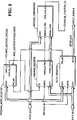
- Referring to Figure 2, the following sequence of events is undertaken for assigning an address to a device whose address is to be programmed. For simplicity, the device will be assumed to be a controller for a disc drive.
- First, the address of the SETUP_REGISTER is placed onto the ADDRESS_BUS, and a specific data word is written onto the DATA_BUS, and thus into the SETUP_REGISTER. The word is specific in that it contains zeros in the fifth and seventh bit positions (i.e., the word is OXOX XXXX, wherein "X" indicates that the digit in the X's position can be either ZERO or ONE and "0" indicates, of course, that the digit is ZERO).
- The SETUP_REGISTER responds to this specific word by actuating the PROGRAM_MODE line in response. This actuation ultimately allows the ADDRESS_REGISTER to receive data, by way of the following sequence: when PROGRAM_MODE_SELECTOR now receives the proper address on the ADDRESS_BUS, PROGRAM_MODE_SELECTOR applies a signal to the line ADDR_RG_CS (an abbreviation for "address register chip select"), which connects to the chip select (CS) line of the ADDRESS_REGISTER. The signal on line CS enables ADDRESS_REGISTER to accept data.
- That is, the "enablement" of ADDRESS_REGISTER for receiving data is actually a two-step process: first, PROGRAM_MODE_SELECTOR is actuated into "program mode," and, after this actuation, receipt of the proper address by PROGRAM_MODE_SELECTOR enables the ADDRESS_REGISTER.
- When in "program mode," PROGRAM_MODE_SELECTOR suspends its normal operation. In normal operation, the PROGRAM MODE SELECTOR inquires whether the data word present on the ADDRESS_BUS is identical to a specific address, namely, that termed MISC_ADDRESS in the Figure. If so, PROGRAM_MODE_SELECTOR actuates the line MISC_ADDRESS_DECODE, which leads to a second device to be enabled (which is distinct from the drive controller in question). During "program mode," however, MISC_ADDRESS_DECODE is constrained to remain de-actuated, and the second device remains disabled.
- At this time, while the ADDRESS,REGISTER is enabled, the ADDRESS_REGISTER accepts and stores data from the DATA BUS, which is the system data bus in the computer. This data is the address assigned to the controller. The ADDRESS_REGISTER presents this data on the bus labeled PRGMD_ADDR (an abbreviation for "programmed address.")
- After being loaded, the ADDRESS_REGISTER also produces a signal on the line ENABLE_IF_PROGRAMMED, which indicates to the ADDRESS_COMPARATOR that the ADDRESS_REGISTER contains data. If the ENABLE_IF_PROGRAMMED line produces no signal, then the ADDRESS_COMPARATOR does not perform the comparison operation (later described) because no address for the device is present.
- The following points of the preceding procedure are emphasized.
- One. The ADDRESS_REGISTER is not addressed directly by the ADDRESS BUS, as is, for example, the SETUP_REGISTER. Instead, the following sequence of data movements is used to enable the ADDRESS_REGISTER for accepting data:
- 1. The SETUP_REGISTER block is addressed (and, of course, write-enabled).
- 2. The specific word OXOX XXXX is written to the SETUP_REGISTER (which actuates line PROGRAM_MODE).
- 3. The block PROGRAM_MODE_SELECTOR is addressed, which actuates line ADDR_RG_CS, because the line PROGRAM_MODE is actuated.
- That is, the sequence of (a) a predetermined address-write, (b) a predetermined data-write, and (c) a second predetermined address-write enables the ADDRESS_REGISTER. In a sense, the "address" of ADDRESS_REGISTER is that of block PROGRAM_MODE_SELECTOR, when in "program mode."
- Two. After the data is written to ADDRESS_REGISTER, the specific word OXOX XXXX is removed from the SETUP_REGISTER, restoring normal functioning of the SETUP_REGISTER.
- During operation of the computer, the ADDRESS COMPARATOR continually compares the address carried by the ADDRESS_BUS with that on PRGMD,ADDR (at the proper periodic time intervals, as dictated by the system clock). When the two addresses match, the ADDRESS COMPARATOR actuates the line SPEC_FUN_CS (an abbreviation for "special function chip select,") thereby actuating the controller in the present example.
- When the word OXOX XXXX is absent from the DATA_BUS, as is the case during normal operation, the SETUP_REGISTER is used as a register for holding information to be sent to peripheral devices during set-up operations, as known in the art, and as indicated by the signal lines in the SETUP_BUS. Further, this absence of the word OXOX XXXX causes line PROGRAM_MODE to be inactive, and thus the Chip Select line (abbreviated CS) prevents data from being written to the ADDRESS_REGISTER block.
- The implementation of the diagram given in Figure 2 is straightforward, as by representing each block (such as the SETUP_REGISTER) by a truth table. Implementation of truth tables in hardware is known in the art. Further, numerous different implementations are possible.
- The device which is enabled by SPECIAL_FUNCTION_CS can be of several types. It can be of the type known as an "expansion card" as that term applies to the expansion slots in a Personal Computer. Alternately, the device can be circuitry located on the main system board, and need not be detachable.
- More generally, the device can be any special function which needs an address in address space. Further, the apparatus of Figure 2, which enables the device, can be contained on the main system board, and yet the special function (which is enabled by the apparatus) need not even be present at the time of manufacture of the main system board. That is, the main system board is equipped with the apparatus of Figure 2, but possibly not with the device which the apparatus is to enable, in anticipation of the later addition of the device. Still further, several apparatus of the type of Figure 2 can be used. In this case, for each, a separate register of the "SETUP_REGISTER" type should be provided, each with a different address [e.g., 93, 94, 95 (hex), etc.]
- In Figure 2, the ADDRESS_COMPARATOR produces the SPECIAL_FUNCTION_CS signal when the address on the ADDRESS BUS matches that held by the ADDRESS_REGISTER. One type of match occurs when the two addresses are identical. However, other types of match can be envisioned, as when the two addresses differ by one.
- That is, the concept of "matching" involves actuation of the SPECIAL_FUNCTION_CS signal in response to placement of a known address on the ADDRESS_BUS. It is not necessary that this address match that in the ADDRESS_REGISTER bit-for-bit, although such matching is perhaps simplest to understand and implement. Instead, it is important that the user know what particular address word will cause the actuation. The ADDRESS_COMPARATOR enables the line SPECIAL_FUNCTION_CS when that address word appears.
- Some of the blocks in Figure 2, such as PROGRAM_MODE_SELECTOR, can be said to "reside" at an address in memory, because that address must be present on the ADDRESS_BUS in order to instruct the block to execute an intended function.
- The described embodiment has a particular advantage in that, where devices other than the CPU may have control of the address and data buses, inadvertent device address writing is prevented by virtue of the described multi-step address writing procedure.
Claims (6)
- A computer system, including processor means coupled to an address bus and a data bus, and peripheral device control means coupled to said address bus and including an address register, characterized in that said peripheral device control means includes addressable selector means coupled to said address bus and adapted to receive a first control signal (PROGRAM MODE), and in response to said first control signal and predetermined address signals on said address bus to provide a second control signal (PROGRAM CS); and in that said address register is coupled to said data bus and in response to said second control signal is adapted to store data on said data bus representing a device address for a peripheral device coupled to said peripheral device control means.
- A computer system according to claim 1, characterized in that said addressable selector means is adapted in the presence of said predetermined address signals on said address bus, and the absence of said first control, to provide an enabling signal for a further device.
- A computer system according to claim 1, or claim 2 characterized in that said peripheral device control means includes addressable register means coupled to said address bus and to said data bus and adapted, in response to address signals on said address bus identifying said addressable register means, and to the presentation of data signals on said data bus representing a predetermined data word (OXOX XXXX), to provide said first control signal.
- A computer system according to claim 3, characterized in that said addressable register means is.adapted, in the presence of said identifying address signals on said address bus, to provide data signals present on said data bus, other than data signals representing said predetermined data word, to said peripheral device during set-up operations.
- A computer system according to any one of the present claims, characterized in that said peripheral device control means includes address comparator means coupled to said address bus and to said address register and adapted, in response to a third control signal provided by said address register when an address is stored therein, to compare addresses provided on said address bus with the address stored in said address register.
- A computer system according to any one of the preceding claims, characterized in that a plurality of said peripheral device control means are provided, response to respective first control signals, to store a respective device address provided on said data bus.
Applications Claiming Priority (2)
| Application Number | Priority Date | Filing Date | Title |
|---|---|---|---|
| US68511991A | 1991-04-15 | 1991-04-15 | |
| US685119 | 1991-04-15 |
Publications (2)
| Publication Number | Publication Date |
|---|---|
| EP0509720A1 true EP0509720A1 (en) | 1992-10-21 |
| EP0509720B1 EP0509720B1 (en) | 1996-04-24 |
Family
ID=24750856
Family Applications (1)
| Application Number | Title | Priority Date | Filing Date |
|---|---|---|---|
| EP19920303213 Expired - Lifetime EP0509720B1 (en) | 1991-04-15 | 1992-04-10 | Peripheral device address control system |
Country Status (3)
| Country | Link |
|---|---|
| EP (1) | EP0509720B1 (en) |
| JP (1) | JPH05173944A (en) |
| DE (1) | DE69210080T2 (en) |
Citations (3)
| Publication number | Priority date | Publication date | Assignee | Title |
|---|---|---|---|---|
| DE2932868A1 (en) * | 1978-08-29 | 1980-03-13 | Schrack Elektrizitaets Ag E | Data processor with central unit connected to peripherals - uses address storage enabling convenient peripheral interchange by use of switching stages each with memory address |
| US4373181A (en) * | 1980-07-30 | 1983-02-08 | Chisholm Douglas R | Dynamic device address assignment mechanism for a data processing system |
| US4964038A (en) * | 1987-10-28 | 1990-10-16 | International Business Machines Corp. | Data processing system having automatic address allocation arrangements for addressing interface cards |
-
1992
- 1992-04-10 DE DE1992610080 patent/DE69210080T2/en not_active Expired - Fee Related
- 1992-04-10 EP EP19920303213 patent/EP0509720B1/en not_active Expired - Lifetime
- 1992-04-14 JP JP11959092A patent/JPH05173944A/en active Pending
Patent Citations (3)
| Publication number | Priority date | Publication date | Assignee | Title |
|---|---|---|---|---|
| DE2932868A1 (en) * | 1978-08-29 | 1980-03-13 | Schrack Elektrizitaets Ag E | Data processor with central unit connected to peripherals - uses address storage enabling convenient peripheral interchange by use of switching stages each with memory address |
| US4373181A (en) * | 1980-07-30 | 1983-02-08 | Chisholm Douglas R | Dynamic device address assignment mechanism for a data processing system |
| US4964038A (en) * | 1987-10-28 | 1990-10-16 | International Business Machines Corp. | Data processing system having automatic address allocation arrangements for addressing interface cards |
Also Published As
| Publication number | Publication date |
|---|---|
| JPH05173944A (en) | 1993-07-13 |
| DE69210080T2 (en) | 1996-12-12 |
| DE69210080D1 (en) | 1996-05-30 |
| EP0509720B1 (en) | 1996-04-24 |
Similar Documents
| Publication | Publication Date | Title |
|---|---|---|
| US5038320A (en) | Computer system with automatic initialization of pluggable option cards | |
| US4373181A (en) | Dynamic device address assignment mechanism for a data processing system | |
| US5274771A (en) | System for configuring an input/output board in a computer | |
| US5524269A (en) | System for activating and configuring an input/output board in a computer | |
| US4964038A (en) | Data processing system having automatic address allocation arrangements for addressing interface cards | |
| EP0281999B1 (en) | Data processing system with pluggable option card | |
| US4080651A (en) | Memory control processor | |
| JP3310006B2 (en) | Computer system | |
| EP0464987A2 (en) | Method and apparatus for initialisation of computer system features | |
| US4080652A (en) | Data processing system | |
| SE9202036D0 (en) | SYSTEM FOR DYNAMICALLY LINKING MODULAR PORTIONS OF COMPUTER SOFTWARE | |
| EP0187453A2 (en) | Program assignable I/O addresses for a computer | |
| EP0545675B1 (en) | Automatic adapter card setup in a computer system | |
| EP0265575B1 (en) | Data processing system having automatic address allocation arrangements for addressing interface cards | |
| US5640594A (en) | Method and system for assigning peripheral device addresses | |
| US6321332B1 (en) | Flexible control of access to basic input/output system memory | |
| EP0509720A1 (en) | Peripheral device address control system | |
| US6205497B1 (en) | System for configuring and input/output board in a computer | |
| JPS5952773A (en) | Dynamically controllable address circuit in automatic test set | |
| JPH0756847A (en) | Portable computer | |
| KR100414922B1 (en) | Device for selecting board of communication module | |
| US4916601A (en) | Means for transferring firmware signals between a control store and a microprocessor means through a reduced number of connections by transfer according to firmware signal function | |
| EP0528773A1 (en) | A system for performing dynamically the configuration of expansion boards on personal computers having a standard bus | |
| EP0488036A1 (en) | Interrupt controller for expansion slots | |
| JPS63197251A (en) | Information processor |
Legal Events
| Date | Code | Title | Description |
|---|---|---|---|
| PUAI | Public reference made under article 153(3) epc to a published international application that has entered the european phase |
Free format text: ORIGINAL CODE: 0009012 |
|
| AK | Designated contracting states |
Kind code of ref document: A1 Designated state(s): DE FR GB |
|
| 17P | Request for examination filed |
Effective date: 19930407 |
|
| 17Q | First examination report despatched |
Effective date: 19930709 |
|
| RAP1 | Party data changed (applicant data changed or rights of an application transferred) |
Owner name: AT&T GLOBAL INFORMATION SOLUTIONS INTERNATIONAL IN |
|
| GRAH | Despatch of communication of intention to grant a patent |
Free format text: ORIGINAL CODE: EPIDOS IGRA |
|
| GRAA | (expected) grant |
Free format text: ORIGINAL CODE: 0009210 |
|
| RIN1 | Information on inventor provided before grant (corrected) |
Inventor name: ISENBERG, W. DAVID |
|
| RAP1 | Party data changed (applicant data changed or rights of an application transferred) |
Owner name: NCR INTERNATIONAL INC. |
|
| AK | Designated contracting states |
Kind code of ref document: B1 Designated state(s): DE FR GB |
|
| REF | Corresponds to: |
Ref document number: 69210080 Country of ref document: DE Date of ref document: 19960530 |
|
| ET | Fr: translation filed | ||
| PLBE | No opposition filed within time limit |
Free format text: ORIGINAL CODE: 0009261 |
|
| STAA | Information on the status of an ep patent application or granted ep patent |
Free format text: STATUS: NO OPPOSITION FILED WITHIN TIME LIMIT |
|
| 26N | No opposition filed | ||
| REG | Reference to a national code |
Ref country code: GB Ref legal event code: IF02 |
|
| REG | Reference to a national code |
Ref country code: GB Ref legal event code: 746 Effective date: 20030402 |
|
| REG | Reference to a national code |
Ref country code: FR Ref legal event code: D6 |
|
| PGFP | Annual fee paid to national office [announced via postgrant information from national office to epo] |
Ref country code: GB Payment date: 20060420 Year of fee payment: 15 |
|
| PGFP | Annual fee paid to national office [announced via postgrant information from national office to epo] |
Ref country code: FR Payment date: 20060428 Year of fee payment: 15 |
|
| PGFP | Annual fee paid to national office [announced via postgrant information from national office to epo] |
Ref country code: DE Payment date: 20060524 Year of fee payment: 15 |
|
| GBPC | Gb: european patent ceased through non-payment of renewal fee |
Effective date: 20070410 |
|
| PG25 | Lapsed in a contracting state [announced via postgrant information from national office to epo] |
Ref country code: DE Free format text: LAPSE BECAUSE OF NON-PAYMENT OF DUE FEES Effective date: 20071101 |
|
| PG25 | Lapsed in a contracting state [announced via postgrant information from national office to epo] |
Ref country code: GB Free format text: LAPSE BECAUSE OF NON-PAYMENT OF DUE FEES Effective date: 20070410 |
|
| PG25 | Lapsed in a contracting state [announced via postgrant information from national office to epo] |
Ref country code: FR Free format text: LAPSE BECAUSE OF NON-PAYMENT OF DUE FEES Effective date: 20070430 |