EP0508073A1 - Cutting insert - Google Patents
Cutting insert Download PDFInfo
- Publication number
- EP0508073A1 EP0508073A1 EP92103105A EP92103105A EP0508073A1 EP 0508073 A1 EP0508073 A1 EP 0508073A1 EP 92103105 A EP92103105 A EP 92103105A EP 92103105 A EP92103105 A EP 92103105A EP 0508073 A1 EP0508073 A1 EP 0508073A1
- Authority
- EP
- European Patent Office
- Prior art keywords
- insert
- chip
- island
- land
- groove
- Prior art date
- Legal status (The legal status is an assumption and is not a legal conclusion. Google has not performed a legal analysis and makes no representation as to the accuracy of the status listed.)
- Granted
Links
- 238000005520 cutting process Methods 0.000 title claims abstract description 49
- 230000007935 neutral effect Effects 0.000 claims description 5
- 238000005245 sintering Methods 0.000 claims description 2
- 239000000463 material Substances 0.000 abstract description 11
- 229910000831 Steel Inorganic materials 0.000 abstract description 5
- 239000010959 steel Substances 0.000 abstract description 5
- 238000003754 machining Methods 0.000 description 9
- 230000008859 change Effects 0.000 description 2
- 230000004048 modification Effects 0.000 description 2
- 238000012986 modification Methods 0.000 description 2
- 230000009471 action Effects 0.000 description 1
- 230000008901 benefit Effects 0.000 description 1
- 238000011161 development Methods 0.000 description 1
- 230000018109 developmental process Effects 0.000 description 1
- 230000000694 effects Effects 0.000 description 1
- 230000006872 improvement Effects 0.000 description 1
- 238000005482 strain hardening Methods 0.000 description 1
Images

Classifications
-
- B—PERFORMING OPERATIONS; TRANSPORTING
- B23—MACHINE TOOLS; METAL-WORKING NOT OTHERWISE PROVIDED FOR
- B23B—TURNING; BORING
- B23B27/00—Tools for turning or boring machines; Tools of a similar kind in general; Accessories therefor
- B23B27/14—Cutting tools of which the bits or tips or cutting inserts are of special material
- B23B27/141—Specially shaped plate-like cutting inserts, i.e. length greater or equal to width, width greater than or equal to thickness
- B23B27/143—Specially shaped plate-like cutting inserts, i.e. length greater or equal to width, width greater than or equal to thickness characterised by having chip-breakers
-
- Y—GENERAL TAGGING OF NEW TECHNOLOGICAL DEVELOPMENTS; GENERAL TAGGING OF CROSS-SECTIONAL TECHNOLOGIES SPANNING OVER SEVERAL SECTIONS OF THE IPC; TECHNICAL SUBJECTS COVERED BY FORMER USPC CROSS-REFERENCE ART COLLECTIONS [XRACs] AND DIGESTS
- Y10—TECHNICAL SUBJECTS COVERED BY FORMER USPC
- Y10T—TECHNICAL SUBJECTS COVERED BY FORMER US CLASSIFICATION
- Y10T407/00—Cutters, for shaping
- Y10T407/23—Cutters, for shaping including tool having plural alternatively usable cutting edges
- Y10T407/235—Cutters, for shaping including tool having plural alternatively usable cutting edges with integral chip breaker, guide or deflector
-
- Y—GENERAL TAGGING OF NEW TECHNOLOGICAL DEVELOPMENTS; GENERAL TAGGING OF CROSS-SECTIONAL TECHNOLOGIES SPANNING OVER SEVERAL SECTIONS OF THE IPC; TECHNICAL SUBJECTS COVERED BY FORMER USPC CROSS-REFERENCE ART COLLECTIONS [XRACs] AND DIGESTS
- Y10—TECHNICAL SUBJECTS COVERED BY FORMER USPC
- Y10T—TECHNICAL SUBJECTS COVERED BY FORMER US CLASSIFICATION
- Y10T407/00—Cutters, for shaping
- Y10T407/24—Cutters, for shaping with chip breaker, guide or deflector
- Y10T407/245—Cutters, for shaping with chip breaker, guide or deflector comprising concave surface in cutting face of tool
Definitions
- the present invention relates to high depth, low force throw away cutting inserts to turn ductile material like steel at low to high cutting speeds and medium to high ranges of feed and depth of cut.
- the present invention further relates to a high depth, low force throw away cutting insert which is capable of withstanding mechanical impact under interrupted machining conditions without effecting the cutting life of the tool.
- the present invention further relates to a high depth, low force throw away cutting insert to turn ductile material which maintains good chip control.
- Chip control inserts are well known in the art where a on the face of the insert adjacent the cutting edge terminates in a ramp shoulder in the flow path of the chip serving to curl an/or break the chip. It is also known in the art to provide a positive rake cutting action serving to decrease power requirements either by tapering the sides extending to the cutting edge or providing a positive rake land on the face perimeter extending from the cutting edge. Special chip breaking effects have been achieved by providing a series of chip deflecting grooves or depressions spaced along the cutting edge such as is disclosed in U.S. Patents Nos. 4,215,957; 4,273,480 and 4,335,984.
- Recess grooves or faces with chip breaking projections are also known in the art, particularly for use in turning operations such as are disclosed in U.S. Patent No. 3,792,514 wherein a uniform concave groove in provided along each cutting edge of the insert for chip breaking in heavy cutting in combination with a nose projection in the concave groove isolated from an island on the insert serving for chip breaking in light cutting operations.
- Another form of such insert is disclosed in U. S. Patent No. 4,214,845 including a pair of chip breaking projections at each corner with another projection on the bisector behind the first projections.
- Another insert is disclosed in U.S. Patent No. 4,626,141 wherein good chip control is achieved, but there is still some improvement to be made in the areas of chip deceleration and wear of the insert during cutting.
- U.S. Patent No. 4,318,645 discloses a polygonal insert of a hard, wear resistant material.
- the insert includes a bump behind each corner of the insert which serves as a chip breaker.
- the bump is separated from the cutting edge land by a lower secondary land which has its maximum height and width in each corner area of the insert. The height and width gradually decrease as the secondary land extends away from the corner area in a direction parallel to the cutting edge.
- U.S. Patent No. 4,626,141 discloses a polygonal shaped chip control insert characterized by a chip control groove extending across the insert corners and along an edge extending from these corners with increasing width away from the cutting corner.
- the groove is formed with a radius extending below a narrow positive rake cutting edge land to a maximum depth tangent with the bottom of the groove.
- the present invention differs from all these developments of the prior art because it offers improved mechanical impact strength which is useful when there are interrupted machining conditions, and allows the insert to turn ductile material such as steel at low to high cutting speeds and medium to high ranges of feed and depth of cut.
- the present invention is directed to a polygonal, throwaway cutting insert which is designed to turn ductile material such as steel at low to high cutting speeds and a medium to high range of feed and depth of cut.
- the insert of the present invention exhibits a chip breaking capability over a wide range of feed and depth of cut.
- the insert may be configured to have a neutral land which is variable in width along the length of the insert.
- the insert is also capable of having a constant land with a concave radius shape instead of the neutral land.
- a cutting insert with a neutral land and variable land width exhibits good wear resistance properties. This is advantageous in that lower cutting forces may be used without sacrificing any machining performance in terms of tool life.
- a cutting insert with a radius land with a variable land width exhibits good impact strength.
- the advantage to that configuration is that the land is well suited to withstand heavy interrupted machining conditions, which conditions induce mechanical impact stress to the insert.
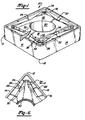
- Figure 1 is a perspective view of the insert of the present invention.
- Figure 2 is a top view of the insert of another embodiment of the present invention using radiused corners.
- Figure 3 is a cut away side view of the insert of the present invention showing the surfaces and chip breakers along line 3-3.
- Figure 4 is a cutaway side view of the insert of the present invention showing the surfaces and chip breakers along line 4-4.
- Figure 5 is a cut away side view of the insert of the present invention showing the surfaces and chip breakers along a line 5-5.
- Figure 6 is a detail of the top view of the embodiment of Figure 1 showing the corner chip breaker surface.
- polygonal lay down indexable insert 10 is configured to have cutting corners 12 and flanks 14.
- Land 16 which may be neutral, variable or contact, may be radiused and runs along the entire perimeter of the insert, thereby forming the initial contact surface to the material to be cut.
- the insert has central island 18 which is provided with a central aperture 20, which is used to secure the insert into position on the tool (not shown) in a manner such as is well known to those of ordinary skill in the art.
- the island may be provided with a countersunk surface proximal to said aperture to minimize the amount of grind stock to be removed as well as to provide minimal warpage of the insert after sintering.
- Entry angle surface 22 is provided around the perimeter of the insert and proximal to land 16.
- the entry angle functions to cause the chip of cutting material along the surface of the insert to start to curl up, thereby providing chip breaking qualities to the insert.
- Groove width variable 24 is located around the periphery of the insert and is proximally located relative to the entry angle 22. Groove width 24 is configured to be of variable width, i.e., narrow towards the corner of the insert and with a wide flank in the middle of the insert.
- Incident angle 26 is provided proximal to chip deceleration pad 28 to aid in chip flow deceleration.
- the deceleration pad aids in controlling the chip.
- the deceleration pad curls and strains the chips at a moderate feed rate and depth of cut to produce acceptable chips during machining. Acceptable chips are those which from during operation which are cut off the work piece and which break off in short pieces so as not to interfere with the machining operation.
- the chip deceleration pad provides an added protection against chipping and cratering of the main island under heavy and interrupted machining conditions.
- the chip deceleration pad is higher off the groove width 24 than the entry angle, and preferably .003 inches higher than the groove.
- the island is provided with an incident angle 30 which serves to break chips formed during the machining operation and further serves to protect the island from fracture, cratering and wear.
- the island surface 32 is higher than the incident angle 30 relative to the groove 24, and preferably is .004 inches higher than the land and .011 higher than the groove.
- the island is further refined by the island primary chip breaker area 34.
- Area 34 is capable of withstanding high mechanical pressure from decelerated chips and its sharp contours serve to break the chips formed during the cutting operation into small, manageable "6" and "9” shaped chips.
- Figure 2 depicts the top plan view of the insert which is contemplated for use when breakage and chipping is a primary feature.
- the corner is provided with a radiused nose portion 36, which gives excellent mechanical strength and is particularly suited for use where there is interrupted machining.
- the entry angle 22 is .022 inches in width
- the corner has an entry angle 38 which is .016 inches in width. It has been surprising that this variation in geometry provides excellent cutting under the conditions previously described, and still affords good mechanical properties.
- the present invention is directed to a polygonal throwaway insert to turn ductile material such as steel at low to high cutting speeds and medium to high ranges of feed and depth of cut.
- the chip breaking capability range of this new insert is somewhere in the range of about 0.014 to 0.040 ipr for feed rate, and 0.040 to 0.350 inches for depth of cut.
- the chip breaker profile taken at the nose portion along line 3-3 is seen in Figure 3.
- the chip breaker consists of a primary positive land 40 and an entry angle which is followed by a secondary positive land 42 and a secondary entry angle. Each entry angle may be any angle, and are, in the present invention, 12 and 27 degrees respectively.
- the purpose of the double land is to provide additional strength to the cutting edge.
- the primary positive land is to lift up the chip at very low ranges of feed and depth of cut. At higher the ranges of feed, the land with the steep entry angles serves to guide the chip into the decleration pad and interrupt its continuous motion for further curling.
- This positive land also functions to minimize friction wear, generating lower cutting forces, lower cutting temperatures, especially when compared to negative rake by other forms of chip breakers.
- Both of these land sections may be either flat or have a radius shape and both sections may form two sides of a triangle or rectangle.
- the width of the whole land is in the range of 0.0185 starting from the cutting edge to the end of the secondary positive land.
- the groove width is 0.0215 inches wide and has a flat bottom.
- the flat bottom may have a radiused shape to form a convex or concave surface.
- the groove serves to change the curling motion of the chip, hence changing its strain hardening level for further breakage.
- the first primary section intersects with the groove bottom at a primary exit angle and intersects with the secondary section to form a secondary exit angle.
- the back wall exists only at the nose section of the cutting point.
- the back wall with its steep differential slope functions to change the chip's strain level in order to curl the chip in a way that the radius of curl is large enough to cause breakage, and the shear stresses are exactly equal to the break stresses, thereby producing acceptable chips at low range of feed and depth of cut.
- the back wall adds strength to the nose area.
- the nose has a symmetrical ridge through the center of the insert at the nose.
- the ridge functions to add strength to the nose section and in some cases aids in curling chips away from the insert.
- the ridge may have rectangular, triangular, cone or convex shape.
- the flank area has the same configuration as that of Figure 3, with the following modification.
- the double positive land forces the chip to undergo different levels of deformation for good chip breakability over the widest applicable ranges of feed and depth of cut.
Landscapes
- Engineering & Computer Science (AREA)
- Mechanical Engineering (AREA)
- Cutting Tools, Boring Holders, And Turrets (AREA)
- Milling Processes (AREA)
Abstract
Description
- The present invention relates to high depth, low force throw away cutting inserts to turn ductile material like steel at low to high cutting speeds and medium to high ranges of feed and depth of cut.
- The present invention further relates to a high depth, low force throw away cutting insert which is capable of withstanding mechanical impact under interrupted machining conditions without effecting the cutting life of the tool.
- The present invention further relates to a high depth, low force throw away cutting insert to turn ductile material which maintains good chip control.
- Chip control inserts are well known in the art where a on the face of the insert adjacent the cutting edge terminates in a ramp shoulder in the flow path of the chip serving to curl an/or break the chip. It is also known in the art to provide a positive rake cutting action serving to decrease power requirements either by tapering the sides extending to the cutting edge or providing a positive rake land on the face perimeter extending from the cutting edge. Special chip breaking effects have been achieved by providing a series of chip deflecting grooves or depressions spaced along the cutting edge such as is disclosed in U.S. Patents Nos. 4,215,957; 4,273,480 and 4,335,984.
- Recess grooves or faces with chip breaking projections are also known in the art, particularly for use in turning operations such as are disclosed in U.S. Patent No. 3,792,514 wherein a uniform concave groove in provided along each cutting edge of the insert for chip breaking in heavy cutting in combination with a nose projection in the concave groove isolated from an island on the insert serving for chip breaking in light cutting operations. Another form of such insert is disclosed in U. S. Patent No. 4,214,845 including a pair of chip breaking projections at each corner with another projection on the bisector behind the first projections. Another insert is disclosed in U.S. Patent No. 4,626,141 wherein good chip control is achieved, but there is still some improvement to be made in the areas of chip deceleration and wear of the insert during cutting.
- McCreery, U.S. Patent No. 4,318,645 discloses a polygonal insert of a hard, wear resistant material. The insert includes a bump behind each corner of the insert which serves as a chip breaker. The bump is separated from the cutting edge land by a lower secondary land which has its maximum height and width in each corner area of the insert. The height and width gradually decrease as the secondary land extends away from the corner area in a direction parallel to the cutting edge.
- Malaker et al., U.S. Patent No. 4,626,141 discloses a polygonal shaped chip control insert characterized by a chip control groove extending across the insert corners and along an edge extending from these corners with increasing width away from the cutting corner. The groove is formed with a radius extending below a narrow positive rake cutting edge land to a maximum depth tangent with the bottom of the groove.
- The present invention differs from all these developments of the prior art because it offers improved mechanical impact strength which is useful when there are interrupted machining conditions, and allows the insert to turn ductile material such as steel at low to high cutting speeds and medium to high ranges of feed and depth of cut.
- It has long been a problem in the art to arrive at a disposable cutting insert which is capable of turning ductile materials and yet be affordable, and offer different feed rates and depths of cut. The present invention meets these long felt needs and offers a chip breaking capability range which is surprising, especially in view of the different feed rates at which the insert is designed to operate.
- It is therefore an object of the present invention to provide for a disposable insert to turn ductile material at low to high cutting speeds and medium to high ranges of feed and depth of cut.
- It is a further object of the present invention to provide a disposable cutting insert which exhibits excellent chip breaking capability over a wide range of feed rates and depths of cut, an lower consumption of cutting forces and horsepower.
- It is a further object of the present invention to provide a cutting insert which exhibits improved wear resistance.
- It is a further object of the present invention to provide for a cutting insert which has excellent impact strength.
- It is a further object of the present invention to provide an insert with a double step island to minimize insert chipping and provide superior chip breaking capabilities.
- Other objects and uses for the cutting inserts of the present invention will become apparent to those of ordinary skill in the art after a reading of the specification and claims.
-
- The present invention is directed to a polygonal, throwaway cutting insert which is designed to turn ductile material such as steel at low to high cutting speeds and a medium to high range of feed and depth of cut. The insert of the present invention exhibits a chip breaking capability over a wide range of feed and depth of cut. The insert may be configured to have a neutral land which is variable in width along the length of the insert. The insert is also capable of having a constant land with a concave radius shape instead of the neutral land. According to the present invention, a cutting insert with a neutral land and variable land width exhibits good wear resistance properties. This is advantageous in that lower cutting forces may be used without sacrificing any machining performance in terms of tool life. A cutting insert with a radius land with a variable land width, as also described by the present invention, exhibits good impact strength. The advantage to that configuration is that the land is well suited to withstand heavy interrupted machining conditions, which conditions induce mechanical impact stress to the insert.
- Figure 1 is a perspective view of the insert of the present invention.
- Figure 2 is a top view of the insert of another embodiment of the present invention using radiused corners.
- Figure 3 is a cut away side view of the insert of the present invention showing the surfaces and chip breakers along line 3-3.
- Figure 4 is a cutaway side view of the insert of the present invention showing the surfaces and chip breakers along line 4-4.
- Figure 5 is a cut away side view of the insert of the present invention showing the surfaces and chip breakers along a line 5-5.
- Figure 6 is a detail of the top view of the embodiment of Figure 1 showing the corner chip breaker surface.
- Turning now to the drawings, wherein like numerals depict like structures, polygonal lay down indexable insert 10 is configured to have cutting
corners 12 andflanks 14.Land 16, which may be neutral, variable or contact, may be radiused and runs along the entire perimeter of the insert, thereby forming the initial contact surface to the material to be cut. The insert hascentral island 18 which is provided with acentral aperture 20, which is used to secure the insert into position on the tool (not shown) in a manner such as is well known to those of ordinary skill in the art. The island may be provided with a countersunk surface proximal to said aperture to minimize the amount of grind stock to be removed as well as to provide minimal warpage of the insert after sintering. -
Entry angle surface 22 is provided around the perimeter of the insert and proximal to land 16. The entry angle functions to cause the chip of cutting material along the surface of the insert to start to curl up, thereby providing chip breaking qualities to the insert.Groove width variable 24 is located around the periphery of the insert and is proximally located relative to theentry angle 22.Groove width 24 is configured to be of variable width, i.e., narrow towards the corner of the insert and with a wide flank in the middle of the insert. -
Incident angle 26 is provided proximal tochip deceleration pad 28 to aid in chip flow deceleration. The deceleration pad aids in controlling the chip. The deceleration pad curls and strains the chips at a moderate feed rate and depth of cut to produce acceptable chips during machining. Acceptable chips are those which from during operation which are cut off the work piece and which break off in short pieces so as not to interfere with the machining operation. In addition, the chip deceleration pad provides an added protection against chipping and cratering of the main island under heavy and interrupted machining conditions. The chip deceleration pad is higher off thegroove width 24 than the entry angle, and preferably .003 inches higher than the groove. - The island is provided with an
incident angle 30 which serves to break chips formed during the machining operation and further serves to protect the island from fracture, cratering and wear. Theisland surface 32 is higher than theincident angle 30 relative to thegroove 24, and preferably is .004 inches higher than the land and .011 higher than the groove. - The island is further refined by the island primary
chip breaker area 34.Area 34 is capable of withstanding high mechanical pressure from decelerated chips and its sharp contours serve to break the chips formed during the cutting operation into small, manageable "6" and "9" shaped chips. - Two embodiments are contemplated within the present invention. Figure 2 depicts the top plan view of the insert which is contemplated for use when breakage and chipping is a primary feature. The corner is provided with a radiused nose portion 36, which gives excellent mechanical strength and is particularly suited for use where there is interrupted machining. By way of example, where the
entry angle 22 is .022 inches in width, the corner has an entry angle 38 which is .016 inches in width. It has been surprising that this variation in geometry provides excellent cutting under the conditions previously described, and still affords good mechanical properties. - The present invention is directed to a polygonal throwaway insert to turn ductile material such as steel at low to high cutting speeds and medium to high ranges of feed and depth of cut. The chip breaking capability range of this new insert is somewhere in the range of about 0.014 to 0.040 ipr for feed rate, and 0.040 to 0.350 inches for depth of cut.
- The chip breaker profile taken at the nose portion along line 3-3 is seen in Figure 3. The chip breaker consists of a primary positive land 40 and an entry angle which is followed by a secondary positive land 42 and a secondary entry angle. Each entry angle may be any angle, and are, in the present invention, 12 and 27 degrees respectively. The purpose of the double land is to provide additional strength to the cutting edge. The primary positive land is to lift up the chip at very low ranges of feed and depth of cut. At higher the ranges of feed, the land with the steep entry angles serves to guide the chip into the decleration pad and interrupt its continuous motion for further curling. This positive land also functions to minimize friction wear, generating lower cutting forces, lower cutting temperatures, especially when compared to negative rake by other forms of chip breakers. Both of these land sections may be either flat or have a radius shape and both sections may form two sides of a triangle or rectangle.
- The width of the whole land is in the range of 0.0185 starting from the cutting edge to the end of the secondary positive land. The groove width is 0.0215 inches wide and has a flat bottom. The flat bottom may have a radiused shape to form a convex or concave surface. The groove serves to change the curling motion of the chip, hence changing its strain hardening level for further breakage. The first primary section intersects with the groove bottom at a primary exit angle and intersects with the secondary section to form a secondary exit angle. The back wall exists only at the nose section of the cutting point. The back wall, with its steep differential slope functions to change the chip's strain level in order to curl the chip in a way that the radius of curl is large enough to cause breakage, and the shear stresses are exactly equal to the break stresses, thereby producing acceptable chips at low range of feed and depth of cut. In addition, the back wall adds strength to the nose area.
- Turning to Figure 4, it can be seen that the nose has a symmetrical ridge through the center of the insert at the nose. The ridge functions to add strength to the nose section and in some cases aids in curling chips away from the insert. The ridge may have rectangular, triangular, cone or convex shape.
- Turning to Figure 5, the flank area has the same configuration as that of Figure 3, with the following modification. The double positive land forces the chip to undergo different levels of deformation for good chip breakability over the widest applicable ranges of feed and depth of cut.
- Various modifications will no doubt occur to those of ordinary skill in the art without departing from the scope and spirit of the invention.
Claims (17)
- A high depth, low force lay down indexable cutting insert, comprising:(a) a polygonal body having cutting corners, flanks and a land along the top periphery of the body;(b) an entry angle surface proximal to said land and extending around the perimeter of the body adjacent to said land;(c) a variable width groove proximal to said entry angle, said groove being progressively narrower toward the corners of the polygonal body and being lower than said land;(d) a polygonal planar island supported on the insert body and raised above the variable width groove, said island having a central aperture therethrough to facilitate securing of the insert onto a tool, said island having a chip breaking angle around its periphery and a primary chip breaker at each of the corners of the polygonal island; and(e) chip deceleration pads at each of said corners of the island, said chip deceleration pad being raised above the variable width groove and lower than said island, said chip deceleration pad abutting said chip breaking angle at the corners of the island on one side and joining the variable land by means of a chip deceleration angle on the other,Whereby, a chip is cut from a work piece at the cutting corner of the insert, enters the insert along the entry angle, is forced against the chip deceleration angle and onto the chip deceleration pad and then onto the chip breaking angle of the island and then into the primary chip breaker area of the island, thereby breaking the chip.
- The insert of claim 1, wherein said cutting corner is radiused to impart improved mechanical impact strength to the insert during operation.
- The insert of claim 1, wherein said land is neutral.
- The insert of claim 1, wherein said land is variable.
- The insert of claim 1, wherein said chip deceleration pad is about .003 inches higher than said groove.
- The insert of claim 1, wherein said island is about .011 inches higher than said groove.
- The insert of claim 1, wherein said island is higher than said land.
- The insert of claim 7, wherein said island is about .004 inches higher than said land.
- The insert of claim of claim 2, wherein said entry angle around the radiused portion is about .016 inches in width and the entry angle around the remainder of the insert is about .022 inches in width.
- The insert of claim 1, wherein said insert operates at a rate of feed of from about 0.014 to 0.040 ipr, and about 0.040 to 0.350 inches for depth of cut.
- The insert of claim 1, wherein said entry angle is about 12 degrees.
- The insert of claim 1, wherein said chip deceleration angle and said chip breaking angle are about 27 degrees.
- The insert of claim 1, wherein said groove is 0.0215 inches wide at it widest point and narrows progressively toward the cutting corners.
- The insert of claim 1, wherein said groove has a flat bottom having a radiused shape.
- The insert of claim 14, wherein said groove bottom radiused shape forms a convex surface.
- The insert of claim 14, wherein said groove bottom forms a concave surface.
- The insert of claim 1, wherein said island is provided with a countersunk surface proximal to said aperture, thereby reducing the grind stock to be removed from the island surface and minimizing warpage to the insert after sintering.
Applications Claiming Priority (2)
| Application Number | Priority Date | Filing Date | Title |
|---|---|---|---|
| US07/664,016 US5193947A (en) | 1991-03-04 | 1991-03-04 | High depth, low force cutting insert |
| US664016 | 1991-03-04 |
Publications (2)
| Publication Number | Publication Date |
|---|---|
| EP0508073A1 true EP0508073A1 (en) | 1992-10-14 |
| EP0508073B1 EP0508073B1 (en) | 1995-05-17 |
Family
ID=24664162
Family Applications (1)
| Application Number | Title | Priority Date | Filing Date |
|---|---|---|---|
| EP92103105A Expired - Lifetime EP0508073B1 (en) | 1991-03-04 | 1992-02-24 | Cutting insert |
Country Status (7)
| Country | Link |
|---|---|
| US (1) | US5193947A (en) |
| EP (1) | EP0508073B1 (en) |
| JP (1) | JP3084317B2 (en) |
| AU (1) | AU1096492A (en) |
| BR (1) | BR9200349A (en) |
| DE (1) | DE69202508T2 (en) |
| ZA (1) | ZA919883B (en) |
Cited By (3)
| Publication number | Priority date | Publication date | Assignee | Title |
|---|---|---|---|---|
| EP0582981A1 (en) * | 1992-08-10 | 1994-02-16 | VALENITE Inc. | Insert for light feed, light depth of cut |
| US5476346A (en) * | 1992-07-02 | 1995-12-19 | Sandvik Ab | Cutting insert for chipforming machining |
| CN104203462A (en) * | 2012-04-17 | 2014-12-10 | 伊斯卡有限公司 | Cutting insert chip-control arrangement |
Families Citing this family (30)
| Publication number | Priority date | Publication date | Assignee | Title |
|---|---|---|---|---|
| DE4136417A1 (en) * | 1991-11-05 | 1993-05-06 | Krupp Widia Gmbh, 4300 Essen, De | CUTTING INSERT |
| SE509362C2 (en) * | 1994-03-18 | 1999-01-18 | Sandvik Ab | Diamond coated body |
| IL111367A0 (en) * | 1994-10-23 | 1994-12-29 | Iscar Ltd | An exchangeable cutting insert |
| US5549424A (en) * | 1994-11-25 | 1996-08-27 | Valenite Inc. | Indexable threading and turning insert with pressed-in chip breakers |
| US5807031A (en) * | 1995-03-10 | 1998-09-15 | Mitsubishi Materials Corp. | Throw-away tip and throw-away type cutter |
| US6026719A (en) * | 1996-10-09 | 2000-02-22 | Li; Xiao Ping | Method of breaking chips and apparatus therefor |
| JP3383543B2 (en) * | 1997-01-31 | 2003-03-04 | 京セラ株式会社 | Cutting insert |
| DE19901456B4 (en) * | 1998-01-19 | 2009-07-09 | Mitsubishi Materials Corp. | Indexable insert |
| USD416917S (en) * | 1998-04-03 | 1999-11-23 | Valenite Inc. | Polygonal indexable cutting insert |
| USD412335S (en) * | 1998-12-18 | 1999-07-27 | Kennametal Inc. | Cutting tool insert |
| US6599061B1 (en) | 2000-08-17 | 2003-07-29 | Kennametal Inc. | Cutting insert with radially aligned chip forming grooves |
| JP3812473B2 (en) * | 2001-11-20 | 2006-08-23 | 三菱マテリアル株式会社 | Throwaway tip |
| WO2008053633A1 (en) * | 2006-10-31 | 2008-05-08 | Kyocera Corporation | Cutting insert |
| JP5239316B2 (en) * | 2007-11-30 | 2013-07-17 | 株式会社タンガロイ | Throwaway tip |
| US8251618B2 (en) * | 2008-11-21 | 2012-08-28 | Kyocera Corporation | Cutting insert, cutting tool, and cutting method using cutting tool |
| AT11676U1 (en) * | 2009-10-02 | 2011-03-15 | Ceratizit Austria Gmbh | CUTTING INSERT FOR A CUTTING TOOL |
| CA2774671A1 (en) * | 2009-10-15 | 2011-04-21 | Tungaloy Corporation | Cutting insert |
| US8967920B2 (en) * | 2011-09-13 | 2015-03-03 | Iscar, Ltd. | Cutting insert and chip-control arrangement therefor |
| US9409237B2 (en) | 2013-09-16 | 2016-08-09 | Iscar, Ltd. | Finish depth turning insert comprising a chip control arrangement |
| CN105899316B (en) * | 2014-03-17 | 2017-10-17 | 住友电工硬质合金株式会社 | Cutting tool |
| US9796024B2 (en) | 2014-04-07 | 2017-10-24 | Kennametal India Limited | Cutting insert with enhanced chip breaking performance |
| US10076788B2 (en) | 2014-05-20 | 2018-09-18 | Iscar, Ltd. | Cutting insert with chip-control arrangement |
| USD739449S1 (en) * | 2014-06-20 | 2015-09-22 | Nicholson Manufacturing Ltd. | Knife tip |
| JP5967330B1 (en) * | 2015-09-25 | 2016-08-10 | 三菱日立ツール株式会社 | Cutting insert and cutting edge exchangeable rotary cutting tool |
| US10583501B2 (en) | 2016-02-05 | 2020-03-10 | Kyocera Corporation | Insert, cutting tool, and method for manufacturing cutting workpiece |
| US10710167B2 (en) | 2017-08-02 | 2020-07-14 | Iscar, Ltd. | Negative finish turning insert with chip forming arrangement |
| US11911828B2 (en) * | 2018-03-27 | 2024-02-27 | Kyocera Corporation | Cutting insert, cutting tool, and method for manufacturing machined product |
| WO2019235084A1 (en) * | 2018-06-08 | 2019-12-12 | 三菱日立ツール株式会社 | Cutting insert and cutting edge replacement type cutting tool |
| WO2020017548A1 (en) * | 2018-07-18 | 2020-01-23 | 京セラ株式会社 | Cutting insert, cutting tool, and method for manufacturing cut workpiece |
| JP6648392B1 (en) * | 2018-09-06 | 2020-02-14 | 住友電工ハードメタル株式会社 | Cutting insert |
Citations (3)
| Publication number | Priority date | Publication date | Assignee | Title |
|---|---|---|---|---|
| DE1912203A1 (en) * | 1968-03-13 | 1969-11-20 | Wickman Wimet Ltd | Cutting insert |
| DE3601759A1 (en) * | 1985-01-23 | 1986-07-24 | GTE Valeron Corp., Danvers, Mass. | CHIP CONTROL |
| EP0332085A2 (en) * | 1987-08-03 | 1989-09-13 | Gte Valenite Corporation | Polygonal cutting insert |
Family Cites Families (12)
| Publication number | Priority date | Publication date | Assignee | Title |
|---|---|---|---|---|
| US3381349A (en) * | 1966-04-25 | 1968-05-07 | Newcomer Prod Inc | Cutting tool |
| JPS4815470U (en) * | 1971-06-29 | 1973-02-21 | ||
| US3947937A (en) * | 1973-11-16 | 1976-04-06 | Karl Hertel | Control groove in cutting elements for metal working tools |
| GB2004477B (en) * | 1977-08-05 | 1982-03-10 | Sumitomo Electric Industries | Throw away insert |
| SE7710434L (en) * | 1977-09-19 | 1979-03-20 | Sandvik Ab | HAPPENS FOR SPANISH WORKING |
| JPS5464384U (en) * | 1977-10-17 | 1979-05-07 | ||
| IL58861A (en) * | 1979-12-04 | 1981-11-30 | Iscar Ltd | Interchangeable insert with a chip breaker |
| US4318645A (en) * | 1980-09-02 | 1982-03-09 | Kennametal Inc. | Cutting insert |
| US4335984A (en) * | 1980-11-05 | 1982-06-22 | Raymond Zweekly | Metalcutting insert for roughing and finishing |
| GB2116082A (en) * | 1982-02-26 | 1983-09-21 | Gen Electric | Inserts for cutting tools |
| USRE32636E (en) * | 1982-09-30 | 1988-04-05 | Gte Valenite Corporation | Cutting insert with chip control |
| US4941780A (en) * | 1987-11-24 | 1990-07-17 | Sumitomo Electric Industries, Ltd. | Indexable cutting insert |
-
1991
- 1991-03-04 US US07/664,016 patent/US5193947A/en not_active Expired - Lifetime
- 1991-12-17 ZA ZA919883A patent/ZA919883B/en unknown
-
1992
- 1992-01-23 BR BR929200349A patent/BR9200349A/en not_active Application Discontinuation
- 1992-02-14 AU AU10964/92A patent/AU1096492A/en not_active Abandoned
- 1992-02-24 DE DE69202508T patent/DE69202508T2/en not_active Expired - Fee Related
- 1992-02-24 EP EP92103105A patent/EP0508073B1/en not_active Expired - Lifetime
- 1992-03-03 JP JP04080346A patent/JP3084317B2/en not_active Expired - Fee Related
Patent Citations (3)
| Publication number | Priority date | Publication date | Assignee | Title |
|---|---|---|---|---|
| DE1912203A1 (en) * | 1968-03-13 | 1969-11-20 | Wickman Wimet Ltd | Cutting insert |
| DE3601759A1 (en) * | 1985-01-23 | 1986-07-24 | GTE Valeron Corp., Danvers, Mass. | CHIP CONTROL |
| EP0332085A2 (en) * | 1987-08-03 | 1989-09-13 | Gte Valenite Corporation | Polygonal cutting insert |
Cited By (4)
| Publication number | Priority date | Publication date | Assignee | Title |
|---|---|---|---|---|
| US5476346A (en) * | 1992-07-02 | 1995-12-19 | Sandvik Ab | Cutting insert for chipforming machining |
| EP0582981A1 (en) * | 1992-08-10 | 1994-02-16 | VALENITE Inc. | Insert for light feed, light depth of cut |
| CN104203462A (en) * | 2012-04-17 | 2014-12-10 | 伊斯卡有限公司 | Cutting insert chip-control arrangement |
| CN104203462B (en) * | 2012-04-17 | 2017-09-12 | 伊斯卡有限公司 | Cutting tip chip control arrangement |
Also Published As
| Publication number | Publication date |
|---|---|
| DE69202508D1 (en) | 1995-06-22 |
| BR9200349A (en) | 1993-01-12 |
| ZA919883B (en) | 1993-06-04 |
| JP3084317B2 (en) | 2000-09-04 |
| US5193947A (en) | 1993-03-16 |
| JPH05104310A (en) | 1993-04-27 |
| EP0508073B1 (en) | 1995-05-17 |
| DE69202508T2 (en) | 1996-02-08 |
| AU1096492A (en) | 1992-09-10 |
Similar Documents
| Publication | Publication Date | Title |
|---|---|---|
| EP0508073B1 (en) | Cutting insert | |
| CA1253329A (en) | Chip control insert | |
| JPH052244Y2 (en) | ||
| US7121772B2 (en) | Cutting insert | |
| US5743681A (en) | Cutting insert with chip control protrusion on a chip surface | |
| US5577867A (en) | Cutter insert | |
| US6234726B1 (en) | Indexable insert | |
| US4507024A (en) | Cutting insert with chip control | |
| US5584616A (en) | Cutting insert | |
| US4685844A (en) | Cutting insert | |
| EP0046874B2 (en) | Cutting insert | |
| US5897272A (en) | Cutting insert having a micro ridge chip breaker | |
| US5000626A (en) | Cutting insert for low ranges of feed and depth of cut | |
| JP3335048B2 (en) | Cutting insert | |
| EP0589265B1 (en) | High sheer, ultra light duty insert | |
| JPS6314964Y2 (en) | ||
| CA2073248C (en) | Cutting insert for light feed rate | |
| GB2035859A (en) | Cutting insert | |
| US5599141A (en) | Chip control insert | |
| CA1176827A (en) | Cutting insert | |
| CA2062125C (en) | High depth, low force cutting insert | |
| CA1210927A (en) | Cutting insert with chip control | |
| USRE32636E (en) | Cutting insert with chip control | |
| JP3782856B2 (en) | Throwaway tip | |
| JPH08294804A (en) | Cutting insert |
Legal Events
| Date | Code | Title | Description |
|---|---|---|---|
| PUAI | Public reference made under article 153(3) epc to a published international application that has entered the european phase |
Free format text: ORIGINAL CODE: 0009012 |
|
| AK | Designated contracting states |
Kind code of ref document: A1 Designated state(s): BE DE FR GB IT NL SE |
|
| 17P | Request for examination filed |
Effective date: 19930224 |
|
| 17Q | First examination report despatched |
Effective date: 19931119 |
|
| RAP1 | Party data changed (applicant data changed or rights of an application transferred) |
Owner name: VALENITE INC. |
|
| GRAA | (expected) grant |
Free format text: ORIGINAL CODE: 0009210 |
|
| AK | Designated contracting states |
Kind code of ref document: B1 Designated state(s): BE DE FR GB IT NL SE |
|
| ET | Fr: translation filed | ||
| REF | Corresponds to: |
Ref document number: 69202508 Country of ref document: DE Date of ref document: 19950622 |
|
| ITF | It: translation for a ep patent filed | ||
| PLBI | Opposition filed |
Free format text: ORIGINAL CODE: 0009260 |
|
| PLBF | Reply of patent proprietor to notice(s) of opposition |
Free format text: ORIGINAL CODE: EPIDOS OBSO |
|
| 26 | Opposition filed |
Opponent name: SANDVIK AKTIEBOLAG MAGNUS ASPEBY PATENT DEPT. Effective date: 19960219 |
|
| NLR1 | Nl: opposition has been filed with the epo |
Opponent name: SANDVIK AKTIEBOLAG MAGNUS ASPEBY PATENT DEPT. |
|
| PLBF | Reply of patent proprietor to notice(s) of opposition |
Free format text: ORIGINAL CODE: EPIDOS OBSO |
|
| PLBF | Reply of patent proprietor to notice(s) of opposition |
Free format text: ORIGINAL CODE: EPIDOS OBSO |
|
| PLBO | Opposition rejected |
Free format text: ORIGINAL CODE: EPIDOS REJO |
|
| PLBN | Opposition rejected |
Free format text: ORIGINAL CODE: 0009273 |
|
| STAA | Information on the status of an ep patent application or granted ep patent |
Free format text: STATUS: OPPOSITION REJECTED |
|
| 27O | Opposition rejected |
Effective date: 19970509 |
|
| NLR2 | Nl: decision of opposition | ||
| PGFP | Annual fee paid to national office [announced via postgrant information from national office to epo] |
Ref country code: NL Payment date: 20010213 Year of fee payment: 10 |
|
| PGFP | Annual fee paid to national office [announced via postgrant information from national office to epo] |
Ref country code: BE Payment date: 20010309 Year of fee payment: 10 |
|
| REG | Reference to a national code |
Ref country code: GB Ref legal event code: IF02 |
|
| PG25 | Lapsed in a contracting state [announced via postgrant information from national office to epo] |
Ref country code: BE Free format text: LAPSE BECAUSE OF NON-PAYMENT OF DUE FEES Effective date: 20020228 |
|
| BERE | Be: lapsed |
Owner name: VALENITE INC. Effective date: 20020228 |
|
| PG25 | Lapsed in a contracting state [announced via postgrant information from national office to epo] |
Ref country code: NL Free format text: LAPSE BECAUSE OF NON-PAYMENT OF DUE FEES Effective date: 20020901 |
|
| NLV4 | Nl: lapsed or anulled due to non-payment of the annual fee |
Effective date: 20020901 |
|
| PGFP | Annual fee paid to national office [announced via postgrant information from national office to epo] |
Ref country code: FR Payment date: 20030210 Year of fee payment: 12 |
|
| PGFP | Annual fee paid to national office [announced via postgrant information from national office to epo] |
Ref country code: SE Payment date: 20040204 Year of fee payment: 13 |
|
| PG25 | Lapsed in a contracting state [announced via postgrant information from national office to epo] |
Ref country code: FR Free format text: LAPSE BECAUSE OF NON-PAYMENT OF DUE FEES Effective date: 20041029 |
|
| REG | Reference to a national code |
Ref country code: FR Ref legal event code: ST |
|
| PGFP | Annual fee paid to national office [announced via postgrant information from national office to epo] |
Ref country code: DE Payment date: 20050217 Year of fee payment: 14 |
|
| PGFP | Annual fee paid to national office [announced via postgrant information from national office to epo] |
Ref country code: GB Payment date: 20050223 Year of fee payment: 14 |
|
| PG25 | Lapsed in a contracting state [announced via postgrant information from national office to epo] |
Ref country code: IT Free format text: LAPSE BECAUSE OF NON-PAYMENT OF DUE FEES;WARNING: LAPSES OF ITALIAN PATENTS WITH EFFECTIVE DATE BEFORE 2007 MAY HAVE OCCURRED AT ANY TIME BEFORE 2007. THE CORRECT EFFECTIVE DATE MAY BE DIFFERENT FROM THE ONE RECORDED. Effective date: 20050224 |
|
| PG25 | Lapsed in a contracting state [announced via postgrant information from national office to epo] |
Ref country code: SE Free format text: LAPSE BECAUSE OF NON-PAYMENT OF DUE FEES Effective date: 20050225 |
|
| REG | Reference to a national code |
Ref country code: FR Ref legal event code: RN |
|
| REG | Reference to a national code |
Ref country code: FR Ref legal event code: FC |
|
| EUG | Se: european patent has lapsed | ||
| PG25 | Lapsed in a contracting state [announced via postgrant information from national office to epo] |
Ref country code: GB Free format text: LAPSE BECAUSE OF NON-PAYMENT OF DUE FEES Effective date: 20060224 |
|
| PG25 | Lapsed in a contracting state [announced via postgrant information from national office to epo] |
Ref country code: DE Free format text: LAPSE BECAUSE OF NON-PAYMENT OF DUE FEES Effective date: 20060901 |
|
| GBPC | Gb: european patent ceased through non-payment of renewal fee |
Effective date: 20060224 |