EP0506925B1 - LOGIK-SYNTHESE mit Analyse des kritischen Pfads - Google Patents
LOGIK-SYNTHESE mit Analyse des kritischen Pfads Download PDFInfo
- Publication number
- EP0506925B1 EP0506925B1 EP91918982A EP91918982A EP0506925B1 EP 0506925 B1 EP0506925 B1 EP 0506925B1 EP 91918982 A EP91918982 A EP 91918982A EP 91918982 A EP91918982 A EP 91918982A EP 0506925 B1 EP0506925 B1 EP 0506925B1
- Authority
- EP
- European Patent Office
- Prior art keywords
- design
- gates
- logic
- gate
- level
- Prior art date
- Legal status (The legal status is an assumption and is not a legal conclusion. Google has not performed a legal analysis and makes no representation as to the accuracy of the status listed.)
- Expired - Lifetime
Links
Images







Classifications
-
- G—PHYSICS
- G06—COMPUTING OR CALCULATING; COUNTING
- G06F—ELECTRIC DIGITAL DATA PROCESSING
- G06F30/00—Computer-aided design [CAD]
- G06F30/30—Circuit design
-
- G—PHYSICS
- G06—COMPUTING OR CALCULATING; COUNTING
- G06F—ELECTRIC DIGITAL DATA PROCESSING
- G06F7/00—Methods or arrangements for processing data by operating upon the order or content of the data handled
Definitions
- the present invention relates generally to computer-aided design and more particularly to a computerized system for designing logic circuits.
- a computerized logic synthesis system for synthesizing a logic circuit design from a functional outline, the system comprising: computer means including means for receiving a functional outline from an operator, a plurality of tunable module generators, each operative to produce a design of one general type of circuits, and critical path analysis means, characterized in that the critical path analysis means comprises means for generating a topology graph with nets drawn as straight lines between gates, the graph depicting a critical path through a synthesized logic circuit, such that in the topology graph, the horizontal coordinate of a gate is set to be proportional to the delay of the longest path from the inputs of the logic circuit to that gate.
- the present invention provides a high level computerized logic synthesis system that synthesizes a complete circuit design based on a functional outline provided by a system designer.
- a system according to the invention includes:
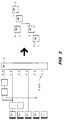
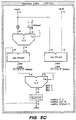
- FIGURE 1 is an illustration of optimization rules utilized by module generators according to the present invention. Optimization rules are pairs of patterns. If the first pattern of a rule matches a fragment of the design, the fragment is repolaced by the second pattern.
- FIG. 2 is an illustration of providing a synthesized, realizable network to replace a functionally-designed logic gate having excess fan-in by means of technology backend according to the present invention.
- a single gate with excessive fan-in is replace by a tree of gates the by the technology backend.
- the fan-in limit is two. The shape of the tree and the points where nets enter it are carefully chosen to avoid increasing delay.
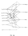
- FIG. 3 illustrates topology graphs showing critical paths through synthesized logic networks.
- delay increases with the x dimension. Displayed are unmapped 16-bit shifters with orgainizations of (16), (4 4), and (2 2 2 2) respectively.
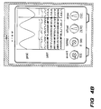
- FIG. 4 illustrates two virtual instruments as presented on a visual display screen of a system according to the invention. Two virtual instruments, the data generator and the data viewer are shown. Presently, the data viewer can present a data bus as an analog wave form or a digital logic scope display.
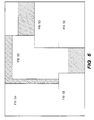
- FIG. 5 illustrates a logic synthesis environment according to the invention.
- the environment illustrates the design and simulation of a digital low-pass filter in this example.
- Logic Synthesis is a new system for digital hardware design which includes many features to speed the development of new products. Design entry and simulation environments have been created which focus the designers attention at the application-level add hide low-level implementation details. Designs, captured as technology-independent block diagrams, are automatically translated to gate-level designs by a collection of module generators plus supporting tools. The high speed of Logic Synthesis encourages experimentation and an iterative design approach.
- Logic Synthesis assists and automates the process of refining digital designs from high level, abstract conceptions to low-level, concrete specifications for their physical implementation.
- Input to Logic Synthesis is expressed as block diagrams, composed of adders, multiplexers, shifters, register files, and so forth.
- Logic Synthesis transforms block diagrams into efficient, electrically and functionally correct, net lists which can be implemented in various technologies.
- Logic Synthesis reduces the time needed to develop a new product. In a competitive market, the time needed to develop a product often has a higher influence on profitability than the product's performance or factory cost. In addition to reducing the design phase of the development schedule, Logic Synthesis can also reduce the debugging and testing phases by eliminating the errors that inevitably occur when a gate-level design is produced manually.
- a disadvantage of the traditional digital design process is that designs are not captured precisely until they have been refined to too low a level of abstraction. At this point, technological dependencies have been introduced and high-level functions have been obscured. Experience has shown that these designs can almost never be reused to take advantage of faster and cheaper technologies when they become available. In contrast, HPLS accepts a high-level, technology-independent design, and automatically maps it to the target technology. Reusing an old design can be as simple as rerunning the synthesis tools.
- Logic Synthesis The initial focus of Logic Synthesis is to assist the design of application specific integrated circuits. ASIC vendors typically provide low-level tools for placement and routing, rule checking, add so forth. Logic Synthesis is intended to complement and augment such tools, rather than duplicate them. Thus, the output of Logic Synthesis is the set of files which a vendor needs to produce an integrated circuit.
- module generators expand the blocks into a generic net list of simple gates.
- a technology backend manipulates the generic net list into a new net list which satisfies the design rules of the target technology, and exploits the technology's special features.
- the heart of Logic Synthesis is a library of module generators, each of which can translate blocks of a single functional type into a collection of simple generic gates.
- the library contains module generators for all the kinds of blocks which are typically used to construct computer data-paths and control logic.
- module generators including: Adders, ALU'S, Comparators, Decrementers, Decoders, Dividers, Encoders, Incrementers, Multipliers, Multiplexers, Random Logic, Register Files, Selectors, Shifters, and State Machines.
- the library is not composed of fixed designs, as are standard cell and gate array libraries; instead, it is composed of generators which can produce an endless variety of fixed designs. For example, blocks are synthesized with exactly the desired operand lengths. By adjusting the parameters given to the module generators, the designer tunes the synthesized circuit to achieve the project's cost and performance objectives. The speed of the synthesis process permits many design choices to be tried, with actual cost and performance data gathered for each. To produce a product upgrade, the current design can be reused, with blocks regenerated using synthesis parameters which yield higher performance. The new product is functionally equivalent to the first; consequently, the need for simulation and testing is reduced.
- the module library includes ripple-carry adders, carry look-ahead adders, and conditional sum adders.
- Multipliers can be synthesized using iterative cellular arrays, or carry-save adder arrays. Best of all, the designer needs little understanding of the alternatives since an are functionally the same and since fast synthesis provides a quick comparison of cost and performance.
- a 16-bit one directional shifter will be considered in detail.
- the shifter has 16-bit input and output data buses. There are also four weighted shift-amount inputs and a shift-in input.
- the library has only one algorithm--it will be implemented as a collection of n-to-l multiplexers.
- the multiplexers There are many possible structural arrangements of the multiplexers, however, which will produce the desired shifter.
- the shifter could be structured as one level of sixteen 16-to-1 multiplexers, or two levels, each composed of sixteen 4-to-1 multiplexers.
- each factorization of the number sixteen yields a different way to structure the shifter.
- the factorization (2 8) corresponds to a shifter with a level of 2-to-1 multiplexers and a level of 8-to-1 multiplexers.
- Table 1 contains data for a selection of structures for the shifter.
- the speed advantage of the (16) structure which is significant in the technology-independent form, becomes less pronounced after the technology back end corrects the excessive fan-in and fan-out.
- Good compromises between gate count and speed are offered by both (2 2 2 2) and (4 4); (2 2 2 2) may be favored in a technology providing only 2-input gates.
- Module generators provide designers with custom produced functional blocks with exactly the required operand sizes. Designers may choose from a large number of functions. Given a function, a number of algorithmic and structural choices are usually available.
- the technology back ends perform two functions: optimization and mapping. Optimization improves the cost and performance of a circuit. Mapping converts the net list of generic gates, produced by the module generators, into an electrically correct net list of gates which can be implemented in the target technology. Mapping is necessary be cause the module generators use gates chosen from a fixed set of functions which may be different from those available in the target technology. Also, the module generators assume gates may have unlimited fan-in and fan-out.
- the technology back ends allow Logic Synthesis to realize an important goal: the ability to implement one design efficiently in multiple technologies.
- Logic Synthesis designs are, in fact, nearly optimal before they reach the technology back ends. Because the implementation of data-path structures, like adders, has evolved to a very high art, and because our module generators have captured that art, circuits produced by the generators typically have excellent fan-in, fan-out, and cost-performance characteristics . For control logic, Logic Synthesis uses generators which include their own optimization algorithms. Since these blocks typically contain relatively few gates, the optimization performed by the module generators is quick and effective.
- a gate with excessive fan-in must be replaced, by the technology backends, with trees of low fan-in gates which implement the same function.
- nets on the critical path should enter the fan-in tree at its root while nets with plenty of slack can enter the tree at a deeper level.
- Slack is a measure of how critical the timing is at a gate or net, with zero slack being most critical. It is defined as the difference between the length of the longest path through the gate or net and the length of the critical path.
- a block diagram object can be a wire or bus connecting two or more modules, the actual module itself, or even a list of logic equations. It may seem ironic that we are encouraging users to use a textual method to specify control logic. We feel, simply, that control logic is more efficiently entered and understood by others as logic equations. Future versions of Logic Synthesis will allow fastidious users to alter the graphical presentation of any block diagram object. In addition, tuning parameters for modules are also specified via the block diagram editor.
- the topology graph presents a gestalt of the design where the entire design is plotted in a single window with nets drawn as straight lines between the gates. Color or line-style is used to indicate slack on the nets, with the critical path highlighted the most.
- Figure 3 is an example of a topology graph.
- a topology graph is constructed in the following manner: Circuit inputs are placed in a column on the left side of the schematic.
- the horizontal coordinate of a gate is set to be proportional to the delay of the longest path from the inputs to that gate.
- Registers appear twice on the diagram. First they are drawn in the input column with only the register outputs shown. They appear again, with only the register inputs drawn, at the right end point of one or more paths through the circuit.
- the Topology Graph is viewed with a Topology Viewer.
- the Topology Viewer allows the designer to view the entire Topology Graph or zoom-in to examine specific regions. High-resolution hard copy can also be obtained. Future versions of the Topology Viewer will allow a designer to point at a specific node (i.e., gate) on the graph and determine what module generated that gate.
- a description of the algorithm used for topology plotting is appended to the specification as Appendix I.
- An integral component of Logic Synthesis is a compiled gate-level simulator that assumes unit delay through all elements.
- the objective of the Simulator is to provide the designer with the means to rapidly verify the logical correctness of the design.
- the performance of the simulator is roughly 1,000,000 gate evaluations per second on an HP-9000/370 workstation (an 8 VAX MIPS machine). Timing verification is best done topologically with tools like the Topology Graph Viewer or with technology-specific timing analysis tools.
- the operation of the Simulator is closely linked to the Data Generator and Data Viewer virtual instruments described below.
- the Data Generator is a means of applying stimuli to the Simulator.
- the Data Generator is modeled after a conventional analog signal generator: there are multiple variable-period waveforms available (e.g., sine, triangle, or square) whose output amplitude is variable and can be biased above or below the zero level.
- the Data Generator's output bus width i.e., quantization
- An additional useful feature is that the output of one generator can be fed into another and summed with its output to produce complex waveforms.
- a planned extension will allow the Data Generator to take its output from a prepared file.
- the Data Viewer is a multi-mode, multi-channel data display instrument.
- the current prototype has two modes implemented.
- the first mode resembles a conventional logic analyzer display with a single high/low display trace per bit of input bus.
- the second mode is an oscilloscope-like analog display where the input data bus is treated as a binary fraction that varies between zero and one. In both modes, the resolution (or trace speed) is variable.
- the Data Viewer automatically increases the number of display channels as more input buses are connected to the instrument. Planned extensions for the Data Viewer include a variable base numeric mode and a character mode.
- the high speed of the simulator makes instruments like the Data Viewer practical and allows the designer to participate in an interactive environment.
- Figure 5 illustrates a logic synthesis session that has progressed to the point of logic simulation.
- the example is that of a simple low-pass filter. Instead of streams of ones and zeros that normally associated with logic simulation, we see waveforms: an appropriate form to view the input and output of a digital filter.
- the major design parameters are indeed parameters. So the designer can, for example, explore the effects of quantization by changing the input bus width parameter and then resynthesizing the design--a process that takes less than a minute.
- the other major parameter is the percentage of the previous output used to compute the next output. Rather than laboriously type the constant and one minus the constant for each trial, the designer has added hardware to the circuit to compute these two values. The constant can then be applied from a data generator and varied in real time while the simulation is progressing.
- the final synthesis can be performed.
- the actual binary constant selected during simulation will be entered.
- the multipliers will also be affected by the optimizer, since each multiplier has a constant as one of its inputs.
- the final task is then to select a particular technology-specific library and perform the technology mapping. For this example, a nine-bit filter, the initial synthesis resulted in a design of 1401 gates. After mapping and optimization, the design was reduced to 649 gates.
- Logic Synthesis provides a set of fast and efficient tools for logic synthesis, simulation, and design visualization.
- the graphical nature of the human interface allows designs to be expressed quickly by the designer. Rapid synthesis and mapping encourage the designer to interactively explore the design space in search of an optimum system configuration. Applying creativity where it will have the greatest impact, the designer remains focused in the application domain, knowing that optimization and mapping into the chosen technology will be automatic. Designs produced by Logic Synthesis are inherently reusable.
- circuit is not partitioned, i.e., for any two gates in the circuit, there is a sequence of nets which connects the two gates.
- MPL most populous level, the level with the most gates.
- MPL-l Call Assign-y-coords-using-loads
- the net list is read from a file.
- An in-memory graph is constructed.
- the nodes in the graph represent the gates in the circuit.
- An edge connects two gates G1 and G2 if a net connects an output of G1 to an input of G2 or a net connects an output of G2 to an input of G1.
- Registers are split into two gates. One has all the inputs from the original gate and no outputs. The other has all the outputs from the original gate and no inputs. It is assumed that this will eliminate all cycles from the graph. ⁇
- Every gate is assigned a level. The level is used as the x-coordinate for plotting the gate. Gates with no inputs are assigned a level of zero. A gate with inputs is assigned a level one greater than the maximum of the levels of the gates which drive its inputs. ⁇
- G-drivers set of gates which 1) drive G and 2) already have been assigned y-coordinates.
- (y-coordinate of G) weighted average of y-coordinates of gates in G-drivers. The average weighs most heavily the gates in G-drivers with levels closest to the level of G. ⁇ ⁇
- G-loads set of gates which 1) are driven by G and 2) already have been assigned y-coordinates.
- ⁇ (y-coordinate of G) weighted average of y-coordinates of gates in G-loads. The average weighs most heavily the gates of G-loads with levels closest to the level of G. ⁇ ⁇ ⁇
- New y-coordinates are assigned which 1) are as close as possible to the preliminary y-coordinates and 2) satisfy the minimum spacing requirement. Any gates which have not been assigned preliminary y-coordinates are ignored (and will be treated on a subsequent pass). ⁇
- a graph edge connects gates G1 and G2, and the level of G2 is greater than the level of G1. Then the slack on the edge is (slack at G2) + (level of G2) - (level of G1) - 1. ⁇
Landscapes
- Engineering & Computer Science (AREA)
- Computer Hardware Design (AREA)
- Physics & Mathematics (AREA)
- Theoretical Computer Science (AREA)
- Evolutionary Computation (AREA)
- Geometry (AREA)
- General Engineering & Computer Science (AREA)
- General Physics & Mathematics (AREA)
- Design And Manufacture Of Integrated Circuits (AREA)
Claims (1)
- Ein computerisiertes Logiksynthesesystem zum Synthetisieren eines Logikschaltungsentwurfs von einer Funktionsskizze, wobei das System folgende Merkmale aufweist: eine Computereinrichtung, die eine Einrichtung zum Empfangen einer Funktionsskizze von einem Betreiber aufweist, eine Mehrzahl von abstimmbaren Modulgeneratoren, von denen jeder wirksam ist, um einen Entwurf eines allgemeinen Typs von Schaltungen zu erzeugen, und eine Kritischer-Weg-Analyseeinrichtung,
dadurch gekennzeichnet,
daß die Kritischer-Weg-Analyseeinrichtung eine Einrichtung zum Erzeugen eines Topologiegraphen mit Netzen, die als gerade Linien zwischen Gattern gezeichnet werden, aufweist, wobei der Graph einen kritischen Weg durch eine synthetisierte Logikschaltung darstellt, derart, daß die Horizontalkoordinate eines Gatters in dem Topologiegraph proportional zur Verzögerung des längsten Wegs von den Eingängen der Logikschaltung zu diesem Gatter eingestellt ist.
Applications Claiming Priority (3)
| Application Number | Priority Date | Filing Date | Title |
|---|---|---|---|
| US59996790A | 1990-10-18 | 1990-10-18 | |
| US599967 | 1990-10-18 | ||
| PCT/US1991/007555 WO1992007333A1 (en) | 1990-10-18 | 1991-10-09 | Logic synthesis |
Publications (2)
| Publication Number | Publication Date |
|---|---|
| EP0506925A1 EP0506925A1 (de) | 1992-10-07 |
| EP0506925B1 true EP0506925B1 (de) | 1996-06-26 |
Family
ID=24401851
Family Applications (1)
| Application Number | Title | Priority Date | Filing Date |
|---|---|---|---|
| EP91918982A Expired - Lifetime EP0506925B1 (de) | 1990-10-18 | 1991-10-09 | LOGIK-SYNTHESE mit Analyse des kritischen Pfads |
Country Status (4)
| Country | Link |
|---|---|
| EP (1) | EP0506925B1 (de) |
| JP (1) | JP3049092B2 (de) |
| DE (1) | DE69120522T2 (de) |
| WO (1) | WO1992007333A1 (de) |
Families Citing this family (3)
| Publication number | Priority date | Publication date | Assignee | Title |
|---|---|---|---|---|
| EP0964345A3 (de) * | 1992-08-26 | 2006-05-03 | Matsushita Electric Industrial Co., Ltd. | Funktion-Entwurfsgerät in einem automatisierten Entwurfssytem für Lsi |
| DE10051077A1 (de) * | 2000-09-22 | 2002-04-18 | Atmel Germany Gmbh | Verfahren zur Charakterisierung und Dokumentation von analogen Schaltungen |
| CN104616557B (zh) * | 2015-01-30 | 2017-05-17 | 南车株洲电力机车有限公司 | 一种轨道车辆模拟电路生成方法、系统及控制方法、系统 |
-
1991
- 1991-10-09 EP EP91918982A patent/EP0506925B1/de not_active Expired - Lifetime
- 1991-10-09 DE DE69120522T patent/DE69120522T2/de not_active Expired - Fee Related
- 1991-10-09 WO PCT/US1991/007555 patent/WO1992007333A1/en not_active Ceased
- 1991-10-09 JP JP3517282A patent/JP3049092B2/ja not_active Expired - Fee Related
Non-Patent Citations (3)
| Title |
|---|
| IEEE Design and Test, December 1986, pages 13-25; H. de Man et al.: "Cathedral-II: A Silicon Compiler for Digital Signal Processing" * |
| Synthesis and Simulation Conf., Kyoto, Japan, Oct. 23rd, 1990; Culbertson et al.: "Hewlett-Packard Logic Synthesis" in "VLSI Logic Synthesis and Design" by R.W. Dutton. * |
| The Electronic System Design Magazine, June 1988, pages 27-34; Eng-Kee Kwang: "Optimized ASICS for the Ears". * |
Also Published As
| Publication number | Publication date |
|---|---|
| DE69120522D1 (de) | 1996-08-01 |
| JPH05503385A (ja) | 1993-06-03 |
| DE69120522T2 (de) | 1996-10-24 |
| WO1992007333A1 (en) | 1992-04-30 |
| EP0506925A1 (de) | 1992-10-07 |
| JP3049092B2 (ja) | 2000-06-05 |
Similar Documents
| Publication | Publication Date | Title |
|---|---|---|
| US6216252B1 (en) | Method and system for creating, validating, and scaling structural description of electronic device | |
| US5553002A (en) | Method and system for creating and validating low level description of electronic design from higher level, behavior-oriented description, using milestone matrix incorporated into user-interface | |
| Luk et al. | Compilation tools for run-time reconfigurable designs | |
| US5910898A (en) | Circuit design methods and tools | |
| US5572436A (en) | Method and system for creating and validating low level description of electronic design | |
| US9009690B1 (en) | Code generation | |
| EP0416669B1 (de) | Logik-Kompilator zum Entwurf von Schaltungsmodellen | |
| US6066178A (en) | Automated design method and system for synthesizing digital multipliers | |
| Hutton et al. | Automatic generation of synthetic sequential benchmark circuits | |
| US7143369B1 (en) | Design partitioning for co-stimulation | |
| Badhoutiya et al. | Field programmable gate array: An extensive review, recent trends, challenges and applications | |
| US7096444B2 (en) | Representing device layout using tree structure | |
| WO1992007333A1 (en) | Logic synthesis | |
| Shirazi et al. | Framework and tools for run-time reconfigurable designs | |
| US5892687A (en) | Don't-- care logic | |
| US7509246B1 (en) | System level simulation models for hardware modules | |
| Mencer et al. | Dynamic circuit generation for Boolean satisfiability in an object-oriented design environment | |
| Guo et al. | An integrated system for developing regular array designs | |
| Fawcett | Tools to speed FPGA development | |
| Reyneri | A Simulink-based hybrid codesign tool for rapid prototyping of FPGA's in signal processing systems | |
| Fang et al. | A multi-level FPGA synthesis method supporting HDL debugging for emulation-based designs | |
| Botros | HDL programming VHDL and Verilog | |
| Sarma et al. | High-level synthesis: Technology transfer to industry | |
| Yan et al. | Hard block reduction and synthesis improvements in Odin II | |
| Bhanu et al. | VLSI design and implementation of a real-time image segmentation processor |
Legal Events
| Date | Code | Title | Description |
|---|---|---|---|
| PUAI | Public reference made under article 153(3) epc to a published international application that has entered the european phase |
Free format text: ORIGINAL CODE: 0009012 |
|
| AK | Designated contracting states |
Kind code of ref document: A1 Designated state(s): DE FR GB NL |
|
| 17P | Request for examination filed |
Effective date: 19921015 |
|
| 17Q | First examination report despatched |
Effective date: 19941121 |
|
| GRAH | Despatch of communication of intention to grant a patent |
Free format text: ORIGINAL CODE: EPIDOS IGRA |
|
| GRAH | Despatch of communication of intention to grant a patent |
Free format text: ORIGINAL CODE: EPIDOS IGRA |
|
| GRAA | (expected) grant |
Free format text: ORIGINAL CODE: 0009210 |
|
| AK | Designated contracting states |
Kind code of ref document: B1 Designated state(s): DE FR GB NL |
|
| REF | Corresponds to: |
Ref document number: 69120522 Country of ref document: DE Date of ref document: 19960801 |
|
| ET | Fr: translation filed | ||
| PLBE | No opposition filed within time limit |
Free format text: ORIGINAL CODE: 0009261 |
|
| STAA | Information on the status of an ep patent application or granted ep patent |
Free format text: STATUS: NO OPPOSITION FILED WITHIN TIME LIMIT |
|
| 26N | No opposition filed | ||
| PGFP | Annual fee paid to national office [announced via postgrant information from national office to epo] |
Ref country code: NL Payment date: 19980921 Year of fee payment: 8 |
|
| PGFP | Annual fee paid to national office [announced via postgrant information from national office to epo] |
Ref country code: GB Payment date: 19981008 Year of fee payment: 8 |
|
| PGFP | Annual fee paid to national office [announced via postgrant information from national office to epo] |
Ref country code: FR Payment date: 19990917 Year of fee payment: 9 |
|
| PGFP | Annual fee paid to national office [announced via postgrant information from national office to epo] |
Ref country code: DE Payment date: 19990920 Year of fee payment: 9 |
|
| PG25 | Lapsed in a contracting state [announced via postgrant information from national office to epo] |
Ref country code: GB Free format text: LAPSE BECAUSE OF NON-PAYMENT OF DUE FEES Effective date: 19991009 |
|
| PG25 | Lapsed in a contracting state [announced via postgrant information from national office to epo] |
Ref country code: NL Free format text: LAPSE BECAUSE OF NON-PAYMENT OF DUE FEES Effective date: 20000501 |
|
| GBPC | Gb: european patent ceased through non-payment of renewal fee |
Effective date: 19991009 |
|
| NLV4 | Nl: lapsed or anulled due to non-payment of the annual fee |
Effective date: 20000501 |
|
| PG25 | Lapsed in a contracting state [announced via postgrant information from national office to epo] |
Ref country code: FR Free format text: LAPSE BECAUSE OF NON-PAYMENT OF DUE FEES Effective date: 20010629 |
|
| PG25 | Lapsed in a contracting state [announced via postgrant information from national office to epo] |
Ref country code: DE Free format text: LAPSE BECAUSE OF NON-PAYMENT OF DUE FEES Effective date: 20010703 |
|
| REG | Reference to a national code |
Ref country code: FR Ref legal event code: ST |