EP0504877A2 - Charging member, charging device, process unit and image forming apparatus having charging member - Google Patents
Charging member, charging device, process unit and image forming apparatus having charging member Download PDFInfo
- Publication number
- EP0504877A2 EP0504877A2 EP92104784A EP92104784A EP0504877A2 EP 0504877 A2 EP0504877 A2 EP 0504877A2 EP 92104784 A EP92104784 A EP 92104784A EP 92104784 A EP92104784 A EP 92104784A EP 0504877 A2 EP0504877 A2 EP 0504877A2
- Authority
- EP
- European Patent Office
- Prior art keywords
- charging
- electrode
- surface layer
- voltage
- charged
- Prior art date
- Legal status (The legal status is an assumption and is not a legal conclusion. Google has not performed a legal analysis and makes no representation as to the accuracy of the status listed.)
- Granted
Links
Images


Classifications
-
- G—PHYSICS
- G03—PHOTOGRAPHY; CINEMATOGRAPHY; ANALOGOUS TECHNIQUES USING WAVES OTHER THAN OPTICAL WAVES; ELECTROGRAPHY; HOLOGRAPHY
- G03G—ELECTROGRAPHY; ELECTROPHOTOGRAPHY; MAGNETOGRAPHY
- G03G15/00—Apparatus for electrographic processes using a charge pattern
- G03G15/02—Apparatus for electrographic processes using a charge pattern for laying down a uniform charge, e.g. for sensitising; Corona discharge devices
- G03G15/0208—Apparatus for electrographic processes using a charge pattern for laying down a uniform charge, e.g. for sensitising; Corona discharge devices by contact, friction or induction, e.g. liquid charging apparatus
- G03G15/0216—Apparatus for electrographic processes using a charge pattern for laying down a uniform charge, e.g. for sensitising; Corona discharge devices by contact, friction or induction, e.g. liquid charging apparatus by bringing a charging member into contact with the member to be charged, e.g. roller, brush chargers
- G03G15/0233—Structure, details of the charging member, e.g. chemical composition, surface properties
-
- G—PHYSICS
- G03—PHOTOGRAPHY; CINEMATOGRAPHY; ANALOGOUS TECHNIQUES USING WAVES OTHER THAN OPTICAL WAVES; ELECTROGRAPHY; HOLOGRAPHY
- G03G—ELECTROGRAPHY; ELECTROPHOTOGRAPHY; MAGNETOGRAPHY
- G03G2221/00—Processes not provided for by group G03G2215/00, e.g. cleaning or residual charge elimination
- G03G2221/16—Mechanical means for facilitating the maintenance of the apparatus, e.g. modular arrangements and complete machine concepts
- G03G2221/1606—Mechanical means for facilitating the maintenance of the apparatus, e.g. modular arrangements and complete machine concepts for the photosensitive element
- G03G2221/1609—Mechanical means for facilitating the maintenance of the apparatus, e.g. modular arrangements and complete machine concepts for the photosensitive element protective arrangements for preventing damage
-
- G—PHYSICS
- G03—PHOTOGRAPHY; CINEMATOGRAPHY; ANALOGOUS TECHNIQUES USING WAVES OTHER THAN OPTICAL WAVES; ELECTROGRAPHY; HOLOGRAPHY
- G03G—ELECTROGRAPHY; ELECTROPHOTOGRAPHY; MAGNETOGRAPHY
- G03G2221/00—Processes not provided for by group G03G2215/00, e.g. cleaning or residual charge elimination
- G03G2221/16—Mechanical means for facilitating the maintenance of the apparatus, e.g. modular arrangements and complete machine concepts
- G03G2221/18—Cartridge systems
- G03G2221/183—Process cartridge
Definitions
- the present invention relates to a charging member, a charging device having the charging member, a process unit having the charging member, and an image forming apparatus having the charging member.
- the charging member is used, for example, to charge a member to be charged such as a photosensitive member or a dielectric member.
- a charging device In order to electrically charge a member, a charging device is known in which a charging member in the form of a roller or the like is contacted to the member to be charged.
- a charging member in the form of a roller or the like is contacted to the member to be charged.
- the charging member may be partly spaced apart, and the charging becomes improper in such a portion.
- the charging member is made of relatively soft material to form a sufficiently wide nip between the member to be charged and the charging member. If the sufficiently wide nip is formed with the use of the soft material, the proper distance is provided between the charging member and the member to be charged outside the nip, and therefore, the improper charging can be avoided.
- a conductive member which is supplied with an oscillating voltage in the form of an AC voltage biased with a DC voltage, and the conductive member is contacted to the member to be charged. More particularly, the charging member is contacted to the photosensitive drum, and the charging member is supplied with an oscillating voltage (Vac + Vdc) in the form of an AC voltage Vac having a peak-to-peak voltage Vpp which is larger than twice the charge starting voltage, biased with a DC voltage Vdc.
- the charging member has been found involving a problem.
- the AC component Vac applied to the electrode 2-3 vibrates the charging member 2 with the result of vibration noise (charging noise).
- a photosensitive drum which comprises a photosensitive layer 1-1, an aluminum base 1-2 which is electrically grounded, and the photosensitive drum 1 is rotated at a speed of 40 mm/sec.
- the charging member 2 Since the charging member 2 is supplied with the AC voltage component, the positive electric charge is induced on the charging member 2-1 side (EPDM or the like in which carbon is dispersed) of the photosensitive layer 1-1, and the negative electric charge is induced on the base layer 1-2 side of the photosensitive drum, as shown by thick line in Figure 10(a), at a certain instance. These electric charges are attracted to each other, and therefore, the surface of the rubber 2-1 is attracted to the photosensitive drum, so that it moves from the position indicated by the thick solid line to the position indicated by the thin solid line.
- the polarity of the AC electric field starts to reverse, the positive charge of the rubber 2-1 and the negative charge in the drum base 1-2 are neutralized by the opposite polarity charge now induced.
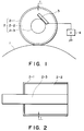
- Figure 1 is a side view of a charging member according to a first embodiment of the present invention.
- FIG. 2 is a front sectional view of the charging member of Figure 1.
- Figure 3A is a side view of a charging member according to a second embodiment of the present invention.
- Figure 3B is a front sectional view of the charging member of Figure 3A.
- Figure 4 is a side view of a charging member according to a third embodiment of the present invention.
- FIG. 5 is a front sectional view of the charging member of Figure 4.
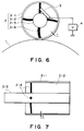
- Figure 6 is a sectional view of the charging member of the third embodiment.
- Figure 7 is a front sectional view of the charging member of Figure 6.
- Figure 8 is a sectional view of a charging member according to a fourth embodiment of the present invention.
- Figure 9 is a sectional view of a process unit including a charging member according to an embodiment of the present invention.
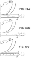
- Figure 10 is a sectional view of a conventional charging member, illustrating the mechanism of noise production during the charging operation.
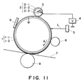
- Figure 11 is a side view of an image forming apparatus according to an embodiment of the present invention.
- an exemplary image forming apparatus according to an embodiment of the present invention. It comprises a photosensitive drum (the member to be charged) including a base layer 1-2 of aluminum which is electrically grounded and a surface photosensitive layer 1-1. It is rotated in the direction A at a peripheral speed of 40 mm/sec.
- the photosensitive layer 1-1 as a negative charging property and is made of organic photoconductor.
- the surface of the photosensitive drum 1 is uniformly charged by a charging roller (charging member) 2 contacted to the surface of the drum 1 and supplied with a voltage. Thereafter, a laser beam L which is modulated in accordance with image information is projected onto the photosensitive drum 1 surface from a laser beam scanner 5, so that an electrostatic latent image is formed.
- the electrostatic latent image is developed by a developing device (developing sleeve 6) with toner into a toner image.
- the thus produced toner image is transferred onto a transfer material 7 by a transfer roller 8 (transfer means).
- the transfer material 7 is introduced into an unshown fixing means, and the toner image is fixed.
- the toner remaining on the photosensitive drum 1 after the image transfer operation is removed by a cleaning blade 9 of a cleaning device, so that the photosensitive drum 1 is prepared for the next image forming operation.
- the charging roller comprises a metal core (electrode) 2-1 made of stainless steel or the like, a surface layer 2-3 made of EPDM (ethylene propylene dien tercopolymer), urethane rubber in which carbon or tin oxide are dispersed as electrically conductive particles, and a cavity 2-2 which is filled with air, nitrogen, argon gas or the like.
- the cavity 2-2 extends in the circumferential direction of the roller 2 adjacent the core metal 2-1. It is preferable that the minimum cross-sectional area in the circumferential direction is not more than 70 % of the maximum.
- the longitudinal sectional configuration of the cavity in the circumferential direction is substantially the same (irrespective of the radial direction), since then the noise does not change when the roller is rotated.
- the surface layer 2-3 is 200 ⁇ m
- the charging roller 2 is press-contacted to the photosensitive drum 1 at a predetermined pressure so that the charging roller 2 is driven by the rotation of the photosensitive drum 1 about a core metal 2-1 which functions as a rotational axis.
- the cavity 2-2 is always formed between the core metal 2-1 and the surface layer 2-3.
- the core metal 2-3 of the charging roller 2 is supplied with a voltage for charging the photosensitive drum 1 from a voltage source 4. More particularly, an oscillating voltage in the form of an AC voltage (peak-to-peak voltage of 2.0 KV and the frequency of 600 Hz) biased with a DC voltage (-700 V) is supplied to the core metal 2-3 through an electrically conductive spring 13.
- the peak-to-peak voltage of the oscillating voltage applied between the photosensitive drum 1 and the charging roller 2 is preferably not less than twice the absolute value of the charge starting voltage of the photosensitive drum 1, from the standpoint of the uniform charging of the photosensitive drum 1. If the peak-to-peak voltage is smaller than twice the charge starting voltage, the charging noise is fairly smaller, but unevenness of the charging in the form of spots result.
- the charge starting voltage is defined as a DC voltage level at which the charging of the photosensitive drum 1 is started when only a DC voltage is applied between the photosensitive drum 1 and the charging roller (charging member) 2.
- the charge starting voltage for the photosensitive drum 1 having an organic photoconductive layer is +560 V.
- the peak-to-peak voltage was 2.0 KV ( ⁇ twice the charge starting voltage), and therefore, the surface of the photosensitive drum 1 was uniformly charged.
- the oscillating voltage is a voltage in which the voltage level periodically changed, and it may be a sine wave, triangular wave or it may be provided by rendering on and off a DC voltage (rectangular wave).
- FIG 2 is a sectional view of the device of Figure 1.
- the charging roller 2 becomes light, and flexible. Therefore, the sufficient large nip width is provided between the charging roller 2 and the photosensitive drum 1, by which the clearance required for proper discharging action is formed between them. Thus, the improper charging can be prevented.
- the charging noise is decreased as compared with the conventional charging roller. This will be understood if the following fact is considered. When a music drum is beaten with light and soft stick made of foamed styrol material, the sound is lower than when it is beaten with a heavy and hard stick.
- the cavity 2-2 is closed by the core metal 2-3 and the surface layer 2-1, the noise produced in the charging member does not leak outside, and therefore, the charging noise is further reduced.
- the electric power supply to the surface layer 2-3 is accomplished by the electric contact between the core metal 2-3 and the voltage supplying-portion extending radially at the longitudinal end of the roller, as shown in Figure 2.
- the power supply portion or portions may be disposed outside a toner image formation area of the photosensitive drum 1 in the longitudinal direction of the charging roller or the photosensitive drum 1, since otherwise the toner may be fused on the photosensitive drum 1 at the power supply portion or portions.
- the device of Figure 11 using the charging roller of Figure 1 and Figure 10 was set in an anechoic chamber, and the noise under the above conditions was measured. The measurements were effected in accordance with paragraph 6 of ISO 7779. In the case of Figure 10 device, the noise was 55 dB, but in the case of Figure 1 charging roller, it was 33 dB.
- the thickness t of the surface layer 2-1 of the charging roller 2 is preferably 10 ⁇ m ⁇ t ⁇ 10000 ⁇ m. If it is not more than 10 ⁇ m the contact between the photosensitive drum 1 and the charging roller 2 is not stabilized with the result of improper charging. If the thickness t of the surface layer 2-1 is not less than 10000 ⁇ m, the charging roller 2 urges the toner particles to the photosensitive drum 1, with the result of the toner fusing on the photosensitive drum 1, which causes improper charging.
- Figures 3A and 3B show another embodiment of the charging roller 2.
- Figure 3B is a sectional view of the device of Figure 3A.
- the cavity 2-2 of the charging member 2 is divided by partition walls substantially perpendicular to the core metal 2-3.
- This structure is effective to avoid reduction of the pressure to the photosensitive drum 1 in the longitudinally central region of the charging member 2.
- the nip width is not reduced in the central portion, and therefore, the improper charging there is not easily occurred.
- the partition wall is made in the form of honeycomb in which the partition walls extend parallel to the core shaft, the charging noise varies each time the partition walls come to the photosensitive drum, with the result of larger charging noise.
- the partition walls substantially perpendicular to the core shaft are preferable.
- the thickness t of the surface layer 2-3 was 200 ⁇ m.
- the measured noise was 38 dB. It is preferable that 10 ⁇ m ⁇ t ⁇ 10000 ⁇ m for the same reasons as described hereinbefore.
- FIG. 4 shows another embodiment of the charging roller 2.
- the reference 2-4 designates a high resistance layer made of hydrin rubber or paper.
- the high resistance layer is effective to prevent abnormal discharging which might occur when the charging roller is contacted to a pin-hole portion of the photosensitive drum 1.
- the high resistance layer preferably has a volume resistivity of 107 - 1010 ⁇ cm.
- a low resistance layer 2-1 has a volume resistivity smaller than that of the high resistance layer, and is made of EPDM or the like containing a relatively large amount of carbon. It is effective to apply the bias voltage from the voltage source 4 to the backside of the high resistance layer 2-4.
- the device further comprises a flange 2-5 made of metal or conductive resin or the like and functions as a voltage or power supply portion for electrically connecting the low resistance layer 2-1 and the core metal 2-3 supplied with the bias voltage.
- the power supply portion or portions 2-5 are preferably outside the toner image formation area of the photosensitive drum 1.
- the high resistance layer and the low resistance layer had thicknesses of 20 microns and 80 microns, respectively. Then, the charging noise was 41 dB which is practically low ( ⁇ 50 dB). As will be understood, the two layer structure is effective to reduce the charging noise, and also to prevent the abnormal discharging even if the photosensitive drum has a pin-hole or another defect.
- the total thickness t of the high resistance layer 2-4 and the low resistance layer 2-1 is preferably 10 ⁇ m ⁇ t ⁇ 10000 ⁇ m, for the same reasons as described hereinbefore.
- the high resistance layer and the low resistance layer may be incorporated in the surface layer of the charging roller of Figure 3.
- FIG. 6 shows a further embodiment, in which the charging member comprises a supporting member made of EPDM or urethane in which a large amount of carbon is dispersed. This is effective to establish the electric connection between the surface layer 2-1 and the core metal 2-3.
- the surface layer had a thickness t of 3 mm.
- the supporting member 2-6 functions to absorb the vibration, and therefore, the core metal 2-3 is not vibrated. Therefore, the beating force to the photosensitive drum is small and therefore, the charging noise is also low.
- FIG 8 shows a further embodiment of the charging member, in which the charging member is in the form of a blade 11. It comprises a blade 11-1 made of EPDM, urethane resin or the like in which carbon, tin oxide or another conductive powder is dispersed, and a cavity 11-2 in the charging blade. It further comprises an electrode 10 for applying a bias voltage for the charging action and a voltage source 4 for applying the voltage to the electrode 10.
- the thickness of the surface layer of the charging blade 11 was 500 microns, and the charging noise was 40 dB.
- a low noise charging member can be provided by the simple structure.
- the pressure of the charging member to the photosensitive drum 1 can be controlled using the rigidity of the charging blade.
- the thickness t of the surface layer of the blade 11 preferably satisfies 10 ⁇ m ⁇ t ⁇ 10000 ⁇ m.
- FIG. 9 shows a process unit U having the charging member described above, according to an embodiment of the present invention.
- the process unit comprises a photosensitive drum 1, a charging roller 2, and a developing sleeve 6.
- the photosensitive drum 1 and the developing sleeve 2 are rotated in the directions indicated by the arrows.
- the photosensitive drum 1 is irradiated with a laser beam L for image formation.
- It further comprises a cleaning blade 9 for removing residual toner from the photosensitive drum 1, a drum shutter 15 for protecting the photosensitive drum from light.
- the developing device contains developer or toner 16.
- the developing device comprises a stirring rod for conveying the toner to the developing sleeve.
- the developing device further comprises a developing blade 13 for applying a uniform thickness layer of the developer on the developing sleeve, a toner container for containing the toner removed by the cleaning blade 9.
- the process unit U is detachably mountable relative to the image forming apparatus.
- the unit may contain at least the image bearing member (photosensitive drum 1) and a charging member (charging roller 2). Because of the structure described above, when the process unit U is mounted in the main assembly of the image forming apparatus, the photosensitive drum 1 is charged by the charging roller with low or no noise, and the electrostatic latent image is formed on the photosensitive member by an imagewisely modulated laser beam L. The thus formed electrostatic latent image is developed by the developing sleeve 6 into a visualized image. The developed image is transferred onto a transfer material by an unshown transfer means, and is conveyed to an image fixing device.
- the process unit which is light, compact and noiseless can be provided.
- the charging polarity of the photosensitive member was negative, but it may be positive.
- the hollow structure of the charging member is effective to suppress the charging noise.
- the reduction of the noise permits the use of higher frequency of the voltage source. This is effective to increase the process speed.
- a charging blade includes an electrode to be supplied with a voltage; a surface layer contactable to a member to be charged; and wherein a cavity is provided between the electrode and the surface layer.
Abstract
Description
- The present invention relates to a charging member, a charging device having the charging member, a process unit having the charging member, and an image forming apparatus having the charging member. The charging member is used, for example, to charge a member to be charged such as a photosensitive member or a dielectric member.
- In order to electrically charge a member, a charging device is known in which a charging member in the form of a roller or the like is contacted to the member to be charged. When the manufacturing accuracy of such a charging roller is not high enough, for example, if the charging roller is eccentric, the charging member may be partly spaced apart, and the charging becomes improper in such a portion. In order to avoid the occurrence of the space, the charging member is made of relatively soft material to form a sufficiently wide nip between the member to be charged and the charging member. If the sufficiently wide nip is formed with the use of the soft material, the proper distance is provided between the charging member and the member to be charged outside the nip, and therefore, the improper charging can be avoided. U.S. Patent No. 4,851,960 which has been assigned to the assignee of this application has proposed that a conductive member is used which is supplied with an oscillating voltage in the form of an AC voltage biased with a DC voltage, and the conductive member is contacted to the member to be charged. More particularly, the charging member is contacted to the photosensitive drum, and the charging member is supplied with an oscillating voltage (Vac + Vdc) in the form of an AC voltage Vac having a peak-to-peak voltage Vpp which is larger than twice the charge starting voltage, biased with a DC voltage Vdc.
- However, the charging member has been found involving a problem. As shown in Figure 10, the AC component Vac applied to the electrode 2-3 vibrates the
charging member 2 with the result of vibration noise (charging noise). - The mechanism of the noise production has been investigated. This will be described referring to Figure 10. In this Figure, designated by a
reference numeral 1 is a photosensitive drum, which comprises a photosensitive layer 1-1, an aluminum base 1-2 which is electrically grounded, and thephotosensitive drum 1 is rotated at a speed of 40 mm/sec. - Since the
charging member 2 is supplied with the AC voltage component, the positive electric charge is induced on the charging member 2-1 side (EPDM or the like in which carbon is dispersed) of the photosensitive layer 1-1, and the negative electric charge is induced on the base layer 1-2 side of the photosensitive drum, as shown by thick line in Figure 10(a), at a certain instance. These electric charges are attracted to each other, and therefore, the surface of the rubber 2-1 is attracted to the photosensitive drum, so that it moves from the position indicated by the thick solid line to the position indicated by the thin solid line. When the polarity of the AC electric field starts to reverse, the positive charge of the rubber 2-1 and the negative charge in the drum base 1-2 are neutralized by the opposite polarity charge now induced. When the AC electric field changes from the positive side to the negative side, the positive charge on the rubber 2-1 and the negative charge on the drum base 1-2 are dissipated. As a result, the surface of the rubber 2-1 returns to the position indicated by the thin solid line (Figure 10(b)). When the negative peak of the AC field is reached, the negative and positive electric charges are induced to the rubber 2-1 side and the drum base 1-2 side, respectively, as shown in Figure 10(c). Then, the rubber 2-1 is moved again from the thick line position to the thin line position. The above-described motions are repeated so that thecharging member 2 vibrates when the AC voltage is supplied. This has been found the cause of the charging noise. As will be understood from the above analysis, thecharging member 2 vibrates twice in one period of the AC voltage, and therefore, the frequency f of the AC voltage and the vibration frequency F of thecharging member 2 have the following relation:

- Accordingly, it is a principal object of the present invention to provide a charging blade, a charging roller, a charging device, a process unit and an image forming apparatus using the charging blade or the charging roller in which the charging noise can be reduced.
- It is another object of the present invention to provide a charging blade, a charging roller, a charging device, a process unit and an image forming apparatus having the charging blade or the charging roller, in which the uniform charging is carried out.
- It is a further object of the present invention to provide a charging blade, a charging roller, a charging device, a process unit and an image forming apparatus having the charging blade or the charging roller in which the sufficient nip is formed between the charging member and the member to be charged, so that the proper charging operation is possible over the entire length of the charging blade or roller.
- These and other objects, features and advantages of the present invention will become more apparent upon a consideration of the following description of the preferred embodiments of the present invention taken in conjunction with the accompanying drawings.
- Figure 1 is a side view of a charging member according to a first embodiment of the present invention.
- Figure 2 is a front sectional view of the charging member of Figure 1.
- Figure 3A is a side view of a charging member according to a second embodiment of the present invention.
- Figure 3B is a front sectional view of the charging member of Figure 3A.
- Figure 4 is a side view of a charging member according to a third embodiment of the present invention.
- Figure 5 is a front sectional view of the charging member of Figure 4.
- Figure 6 is a sectional view of the charging member of the third embodiment.
- Figure 7 is a front sectional view of the charging member of Figure 6.
- Figure 8 is a sectional view of a charging member according to a fourth embodiment of the present invention.
- Figure 9 is a sectional view of a process unit including a charging member according to an embodiment of the present invention.
- Figure 10 is a sectional view of a conventional charging member, illustrating the mechanism of noise production during the charging operation.
- Figure 11 is a side view of an image forming apparatus according to an embodiment of the present invention.
- Referring to the accompanying drawings, the preferred embodiments of the present invention will be described.
- Referring first to Figure 11, there is shown an exemplary image forming apparatus according to an embodiment of the present invention. It comprises a photosensitive drum (the member to be charged) including a base layer 1-2 of aluminum which is electrically grounded and a surface photosensitive layer 1-1. It is rotated in the direction A at a peripheral speed of 40 mm/sec. In this embodiment, the photosensitive layer 1-1 as a negative charging property and is made of organic photoconductor.
- The surface of the
photosensitive drum 1 is uniformly charged by a charging roller (charging member) 2 contacted to the surface of thedrum 1 and supplied with a voltage. Thereafter, a laser beam L which is modulated in accordance with image information is projected onto thephotosensitive drum 1 surface from alaser beam scanner 5, so that an electrostatic latent image is formed. The electrostatic latent image is developed by a developing device (developing sleeve 6) with toner into a toner image. The thus produced toner image is transferred onto atransfer material 7 by a transfer roller 8 (transfer means). - After the image transfer, the
transfer material 7 is introduced into an unshown fixing means, and the toner image is fixed. - On the other hand, the toner remaining on the
photosensitive drum 1 after the image transfer operation, is removed by acleaning blade 9 of a cleaning device, so that thephotosensitive drum 1 is prepared for the next image forming operation. - Referring to Figure 1, the description will be made as to the charging member according to an embodiment of the present invention. The charging roller comprises a metal core (electrode) 2-1 made of stainless steel or the like, a surface layer 2-3 made of EPDM (ethylene propylene dien tercopolymer), urethane rubber in which carbon or tin oxide are dispersed as electrically conductive particles, and a cavity 2-2 which is filled with air, nitrogen, argon gas or the like. The cavity 2-2 extends in the circumferential direction of the
roller 2 adjacent the core metal 2-1. It is preferable that the minimum cross-sectional area in the circumferential direction is not more than 70 % of the maximum. Furthermore, as shown in Figures 1 and 2, it is preferable that the longitudinal sectional configuration of the cavity in the circumferential direction is substantially the same (irrespective of the radial direction), since then the noise does not change when the roller is rotated. In this embodiment, the surface layer 2-3 is 200 µm Thecharging roller 2 is press-contacted to thephotosensitive drum 1 at a predetermined pressure so that thecharging roller 2 is driven by the rotation of thephotosensitive drum 1 about a core metal 2-1 which functions as a rotational axis. When the surface of the photosensitive drum is sequentially charged by the charging roller, the cavity 2-2 is always formed between the core metal 2-1 and the surface layer 2-3. - The core metal 2-3 of the
charging roller 2 is supplied with a voltage for charging thephotosensitive drum 1 from avoltage source 4. More particularly, an oscillating voltage in the form of an AC voltage (peak-to-peak voltage of 2.0 KV and the frequency of 600 Hz) biased with a DC voltage (-700 V) is supplied to the core metal 2-3 through an electricallyconductive spring 13. Here, the peak-to-peak voltage of the oscillating voltage applied between thephotosensitive drum 1 and thecharging roller 2 is preferably not less than twice the absolute value of the charge starting voltage of thephotosensitive drum 1, from the standpoint of the uniform charging of thephotosensitive drum 1. If the peak-to-peak voltage is smaller than twice the charge starting voltage, the charging noise is fairly smaller, but unevenness of the charging in the form of spots result. Microscopically, the contact surfaces of the chargingmember 2 and thephotosensitive drum 1 involve fine pits and projections, and therefore, ideal surface to surface contact can not be provided. If the peak-to-peak voltage is smaller than twice the charge starting voltage, the uniforming effect is not provided. The produced spots appear in the resultant image, thus deteriorating the image quality. The charge starting voltage is defined as a DC voltage level at which the charging of thephotosensitive drum 1 is started when only a DC voltage is applied between thephotosensitive drum 1 and the charging roller (charging member) 2. In this embodiment, the charge starting voltage for thephotosensitive drum 1 having an organic photoconductive layer is +560 V. In this embodiment, the peak-to-peak voltage was 2.0 KV (≧ twice the charge starting voltage), and therefore, the surface of thephotosensitive drum 1 was uniformly charged. The oscillating voltage is a voltage in which the voltage level periodically changed, and it may be a sine wave, triangular wave or it may be provided by rendering on and off a DC voltage (rectangular wave). - Figure 2 is a sectional view of the device of Figure 1. As will be understood from Figure 2, there is a cavity 2-2 in the charging
roller 2, and therefore, the chargingroller 2 becomes light, and flexible. Therefore, the sufficient large nip width is provided between the chargingroller 2 and thephotosensitive drum 1, by which the clearance required for proper discharging action is formed between them. Thus, the improper charging can be prevented. The charging noise is decreased as compared with the conventional charging roller. This will be understood if the following fact is considered. When a music drum is beaten with light and soft stick made of foamed styrol material, the sound is lower than when it is beaten with a heavy and hard stick. - In addition, the cavity 2-2 is closed by the core metal 2-3 and the surface layer 2-1, the noise produced in the charging member does not leak outside, and therefore, the charging noise is further reduced. The electric power supply to the surface layer 2-3 is accomplished by the electric contact between the core metal 2-3 and the voltage supplying-portion extending radially at the longitudinal end of the roller, as shown in Figure 2.
- The power supply portion or portions may be disposed outside a toner image formation area of the
photosensitive drum 1 in the longitudinal direction of the charging roller or thephotosensitive drum 1, since otherwise the toner may be fused on thephotosensitive drum 1 at the power supply portion or portions. - The device of Figure 11 using the charging roller of Figure 1 and Figure 10 was set in an anechoic chamber, and the noise under the above conditions was measured. The measurements were effected in accordance with
paragraph 6 of ISO 7779. In the case of Figure 10 device, the noise was 55 dB, but in the case of Figure 1 charging roller, it was 33 dB. - The thickness t of the surface layer 2-1 of the charging
roller 2 is preferably 10 µm < t < 10000 µm. If it is not more than 10 µm the contact between thephotosensitive drum 1 and the chargingroller 2 is not stabilized with the result of improper charging. If the thickness t of the surface layer 2-1 is not less than 10000 µm, the chargingroller 2 urges the toner particles to thephotosensitive drum 1, with the result of the toner fusing on thephotosensitive drum 1, which causes improper charging. - Figures 3A and 3B show another embodiment of the charging
roller 2. Figure 3B is a sectional view of the device of Figure 3A. In this embodiment, as shown in Figure 3B, the cavity 2-2 of the chargingmember 2 is divided by partition walls substantially perpendicular to the core metal 2-3. This structure is effective to avoid reduction of the pressure to thephotosensitive drum 1 in the longitudinally central region of the chargingmember 2. As a result, the nip width is not reduced in the central portion, and therefore, the improper charging there is not easily occurred. When the partition wall is made in the form of honeycomb in which the partition walls extend parallel to the core shaft, the charging noise varies each time the partition walls come to the photosensitive drum, with the result of larger charging noise. Therefore, it has been found that the partition walls substantially perpendicular to the core shaft are preferable. In this embodiment, the thickness t of the surface layer 2-3 was 200 µm. The measured noise was 38 dB. It is preferable that 10 µm < t < 10000 µm for the same reasons as described hereinbefore. - Figure 4 shows another embodiment of the charging
roller 2. In this embodiment, the reference 2-4 designates a high resistance layer made of hydrin rubber or paper. The high resistance layer is effective to prevent abnormal discharging which might occur when the charging roller is contacted to a pin-hole portion of thephotosensitive drum 1. The high resistance layer preferably has a volume resistivity of 10⁷ - 10¹⁰ Ωcm. A low resistance layer 2-1 has a volume resistivity smaller than that of the high resistance layer, and is made of EPDM or the like containing a relatively large amount of carbon. It is effective to apply the bias voltage from thevoltage source 4 to the backside of the high resistance layer 2-4. The device further comprises a flange 2-5 made of metal or conductive resin or the like and functions as a voltage or power supply portion for electrically connecting the low resistance layer 2-1 and the core metal 2-3 supplied with the bias voltage. The power supply portion or portions 2-5 are preferably outside the toner image formation area of thephotosensitive drum 1. - In this embodiment, the high resistance layer and the low resistance layer had thicknesses of 20 microns and 80 microns, respectively. Then, the charging noise was 41 dB which is practically low (< 50 dB). As will be understood, the two layer structure is effective to reduce the charging noise, and also to prevent the abnormal discharging even if the photosensitive drum has a pin-hole or another defect. The total thickness t of the high resistance layer 2-4 and the low resistance layer 2-1 is preferably 10 µm < t < 10000 µm, for the same reasons as described hereinbefore. The high resistance layer and the low resistance layer may be incorporated in the surface layer of the charging roller of Figure 3.
- Figure 6 shows a further embodiment, in which the charging member comprises a supporting member made of EPDM or urethane in which a large amount of carbon is dispersed. This is effective to establish the electric connection between the surface layer 2-1 and the core metal 2-3. In this embodiment, the surface layer had a thickness t of 3 mm. In this case, even if the surface layer is vibrated, the supporting member 2-6 functions to absorb the vibration, and therefore, the core metal 2-3 is not vibrated. Therefore, the beating force to the photosensitive drum is small and therefore, the charging noise is also low.
- With this structure, the nip between the charging member and the photosensitive drum is assured, and therefore, even if the force applied to the core metal 2-3 is made stronger, the end deformation is small so that the uniform nip can be provided over the entire longitudinal length, because the flexibility at the end portions of the charging
roller 2 is large. - Figure 8 shows a further embodiment of the charging member, in which the charging member is in the form of a blade 11. It comprises a blade 11-1 made of EPDM, urethane resin or the like in which carbon, tin oxide or another conductive powder is dispersed, and a cavity 11-2 in the charging blade. It further comprises an
electrode 10 for applying a bias voltage for the charging action and avoltage source 4 for applying the voltage to theelectrode 10. - In this embodiment, the thickness of the surface layer of the charging blade 11 was 500 microns, and the charging noise was 40 dB.
- In this case, a low noise charging member can be provided by the simple structure. In addition, the pressure of the charging member to the
photosensitive drum 1 can be controlled using the rigidity of the charging blade. The thickness t of the surface layer of the blade 11 preferably satisfies 10 µm < t < 10000 µm. - Figure 9 shows a process unit U having the charging member described above, according to an embodiment of the present invention. The process unit comprises a
photosensitive drum 1, a chargingroller 2, and a developingsleeve 6. Thephotosensitive drum 1 and the developingsleeve 2 are rotated in the directions indicated by the arrows. Thephotosensitive drum 1 is irradiated with a laser beam L for image formation. It further comprises acleaning blade 9 for removing residual toner from thephotosensitive drum 1, adrum shutter 15 for protecting the photosensitive drum from light. The developing device contains developer ortoner 16. The developing device comprises a stirring rod for conveying the toner to the developing sleeve. The developing device further comprises a developingblade 13 for applying a uniform thickness layer of the developer on the developing sleeve, a toner container for containing the toner removed by thecleaning blade 9. - The process unit U is detachably mountable relative to the image forming apparatus. The unit may contain at least the image bearing member (photosensitive drum 1) and a charging member (charging roller 2). Because of the structure described above, when the process unit U is mounted in the main assembly of the image forming apparatus, the
photosensitive drum 1 is charged by the charging roller with low or no noise, and the electrostatic latent image is formed on the photosensitive member by an imagewisely modulated laser beam L. The thus formed electrostatic latent image is developed by the developingsleeve 6 into a visualized image. The developed image is transferred onto a transfer material by an unshown transfer means, and is conveyed to an image fixing device. - As described hereinbefore, according to the present invention, the process unit which is light, compact and noiseless can be provided.
- In the foregoing embodiments, the charging polarity of the photosensitive member was negative, but it may be positive.
- Thus, the hollow structure of the charging member is effective to suppress the charging noise. According to the present invention, the reduction of the noise permits the use of higher frequency of the voltage source. This is effective to increase the process speed.
- While the invention has been described with reference to the structures disclosed herein, it is not confined to the details set forth and this application is intended to cover such modifications or changes as may come within the purposes of the improvements or the scope of the following claims.
- A charging blade includes an electrode to be supplied with a voltage; a surface layer contactable to a member to be charged; and wherein a cavity is provided between the electrode and the surface layer.
Claims (29)
- A charging blade comprising:
an electrode to be supplied with a voltage;
a surface layer contactable to a member to be charged; and
wherein a cavity is provided between said electrode and said surface layer. - A charging blade according to Claim 1, wherein said surface layer has a thickness t satisfying 10 µm < t < 10000 µm.
- A charging blade according to Claim 1, further comprising a power supply portion for supplying the voltage to said surface layer through said electrode.
- A charging roller comprising:
an electrode to be supplied with a voltage;
a surface layer contactable to a member to be charged; and
wherein a cavity extending in a circumferential direction of said charging roller between said electrode member and said surface layer. - A charging roller according to Claim 4, wherein said surface layer has a thickness t satisfying 10 µm < t < 10000 µm.
- A charging roller according to Claim 4, wherein said electrode member constitutes a shaft for said charging roller.
- A charging roller according to Claim 4, wherein said cavity is disposed adjacent said electrode.
- A charging roller according to Claim 4, wherein said cavity is sealed.
- A charging roller according to Claim 4 or 8, further comprising a power supply portion for supplying the voltage to said surface layer through said electrode.
- A charging roller according to Claim 9, wherein said power supply portion is disposed adjacent a longitudinal end of said charging roller.
- A charging roller according to Claim 4, wherein said cavity has substantially the same configuration in any longitudinal cross-section along an axis thereof.
- A charging roller according to Claim 4, wherein said surface layer comprises a first resistance layer to be contacted to the member to be charged and having a first volume resistivity and a second resistance layer inside the first resistance layer and having a second volume resistivity smaller than the first volume resistivity.
- A charging device comprising:
a charging member continuously charging a surface of a member to be charged;
said charging member including an electrode to be supplied with a voltage and a surface layer contactable to the member to be charged, wherein a cavity is provided between said electrode and said surface layer, and wherein said cavity is always present between said electrode member and said surface layer while the surface is continuously charged by said charging member. - A device according to Claim 13, further comprising voltage applying means for applying a voltage between the member to be charged and said electrode, and the voltage includes oscillating component.
- A device according to Claim 14, wherein the oscillating component have a peak-to-peak voltage which is not less than twice and absolute value of a charge starting voltage relative to the member to be charged.
- A device according to Claim 13, wherein said surface layer has a thickness t satisfying 10 µm < t < 10000 µm.
- A device according to Claim 13, wherein said cavity is disposed adjacent said electrode.
- A device according to Claim 13, wherein said cavity is sealed.
- A device according to Claim 13 or 18, wherein said charging member has a power supply portion for supplying a voltage to said surface layer through said electrode.
- A device according to Claim 19, wherein said power supply portion is disposed adjacent a longitudinal end of said charging member.
- A device according to Claim 13, wherein said surface layer includes a first resistance layer contactable to the member to be charged and having a first volume resistivity and a second resistance layer inside said first resistance layer and having a second volume resistivity which is smaller than the first volume resistivity.
- A device according to Claim 13, wherein said charging member is in the form of a roller.
- A device according to Claim 13, wherein said charging member is in the form of a blade.
- A device according to Claim 22, wherein said cavity has substantially the same configuration in any longitudinal section including an axis of said charging member.
- A process unit detachably mountable to an image forming apparatus, comprising:
a member to be charged in the form of an image bearing member;
a charging member continuously charging a surface of the member to be charged;
said charging member including an electrode to be supplied with a voltage and a surface layer contactable to the member to be charged, wherein a cavity is provided between said electrode and said surface layer, and wherein said cavity is always present between said electrode member and said surface layer while the surface is continuously charged by said charging member. - An image forming apparatus comprising:
a member to be charged in the form of an image bearing member;
image forming means for forming an image on said member;
a charging member continuously charging a surface of the member to be charged;
said charging member including an electrode to be supplied with a voltage and a surface layer contactable to the member to be charged, wherein a cavity is provided between said electrode and said surface layer, and wherein said cavity is always present between said electrode member and said surface layer while the surface is continuously charged by said charging member. - A device according to Claim 26, further comprising voltage applying means for applying a voltage between the member to be charged and said electrode, and the voltage includes oscillating component.
- A device according to Claim 27, wherein the oscillating component have a peak-to-peak voltage which is not less than twice and absolute value of a charge starting voltage relative to the member to be charged.
- A device according to Claim 26, wherein said surface layer has a thickness t satisfying 10 µm < t < 10000 µm.
Applications Claiming Priority (3)
| Application Number | Priority Date | Filing Date | Title |
|---|---|---|---|
| JP3056859A JP2899123B2 (en) | 1991-03-20 | 1991-03-20 | Charging member, charging device, image forming apparatus provided with this charging device, and process unit detachable from this image forming device |
| JP56859/91 | 1991-03-20 | ||
| JP5685991 | 1991-03-20 |
Publications (3)
| Publication Number | Publication Date |
|---|---|
| EP0504877A2 true EP0504877A2 (en) | 1992-09-23 |
| EP0504877A3 EP0504877A3 (en) | 1993-07-07 |
| EP0504877B1 EP0504877B1 (en) | 2003-06-04 |
Family
ID=13039143
Family Applications (1)
| Application Number | Title | Priority Date | Filing Date |
|---|---|---|---|
| EP92104784A Expired - Lifetime EP0504877B1 (en) | 1991-03-20 | 1992-03-19 | Charging device, process unit and image forming apparatus having a charging device |
Country Status (5)
| Country | Link |
|---|---|
| US (1) | US5541711A (en) |
| EP (1) | EP0504877B1 (en) |
| JP (1) | JP2899123B2 (en) |
| DE (1) | DE69233089T2 (en) |
| HK (1) | HK1011845A1 (en) |
Cited By (2)
| Publication number | Priority date | Publication date | Assignee | Title |
|---|---|---|---|---|
| EP0590912A2 (en) * | 1992-09-28 | 1994-04-06 | Mita Industrial Co., Ltd. | Method of contact-charging the surface of a photosensitive material |
| EP0622704A2 (en) * | 1993-04-28 | 1994-11-02 | Canon Kabushiki Kaisha | Charging member, charging device, process cartridge and image forming apparatus |
Families Citing this family (11)
| Publication number | Priority date | Publication date | Assignee | Title |
|---|---|---|---|---|
| US5914742A (en) * | 1996-11-27 | 1999-06-22 | Lexmark International, Inc. | Primary charge roller with protruding end |
| JP3473742B2 (en) * | 1998-02-03 | 2003-12-08 | シャープ株式会社 | Charge supply device and image forming apparatus |
| US6859627B2 (en) | 1998-12-28 | 2005-02-22 | Canon Kabushiki Kaisha | Image developing apparatus, process cartridge, electrophotographic image forming apparatus, and developing unit frame |
| JP3363873B2 (en) | 1999-07-13 | 2003-01-08 | キヤノン株式会社 | Method for sequentially displaying developer amount and electrophotographic image forming apparatus |
| JP2001051490A (en) | 1999-08-06 | 2001-02-23 | Canon Inc | Developing device, process cartridge and electrophotographic image forming device |
| US6912366B1 (en) * | 1999-08-31 | 2005-06-28 | Canon Kabushiki Kaisha | Image forming apparatus comprising means for detecting an amount of developer contained in a developer container, a memory for storing the amount detected by the detecting means, and control means for updating the information stored in the memory |
| JP2001194890A (en) | 1999-10-27 | 2001-07-19 | Canon Inc | Developer amount display method and electrphotographic image forming device |
| JP2001255786A (en) | 2000-01-07 | 2001-09-21 | Canon Inc | Electrophotographic image forming device |
| JP2002072573A (en) | 2000-08-23 | 2002-03-12 | Canon Inc | Image-forming device, cartridge image-forming system and storage medium |
| JP2004038034A (en) * | 2002-07-05 | 2004-02-05 | Ricoh Co Ltd | Charging device, process cartridge, image forming apparatus, and copying machine |
| JP7034815B2 (en) * | 2017-04-27 | 2022-03-14 | キヤノン株式会社 | Charging member, electrophotographic process cartridge and electrophotographic image forming apparatus |
Citations (6)
| Publication number | Priority date | Publication date | Assignee | Title |
|---|---|---|---|---|
| JPS6023874A (en) * | 1983-07-19 | 1985-02-06 | Canon Inc | Cleaning device |
| JPS60147756A (en) * | 1984-01-13 | 1985-08-03 | Toshiba Corp | Charging device |
| JPS63208879A (en) * | 1987-02-26 | 1988-08-30 | Canon Inc | Contact electric charger |
| EP0308185A2 (en) * | 1987-09-14 | 1989-03-22 | Canon Kabushiki Kaisha | A charging device |
| US4823689A (en) * | 1986-03-18 | 1989-04-25 | Canon Kabushiki Kaisha | Elastic roller with internal openings for use with image forming apparatus |
| JPH01179957A (en) * | 1988-01-11 | 1989-07-18 | Canon Inc | Contact electrostatic charger |
Family Cites Families (4)
| Publication number | Priority date | Publication date | Assignee | Title |
|---|---|---|---|---|
| US4851960A (en) * | 1986-12-15 | 1989-07-25 | Canon Kabushiki Kaisha | Charging device |
| CN1038277C (en) * | 1987-12-28 | 1998-05-06 | 佳能公司 | Imaging device |
| JPH0789249B2 (en) * | 1989-09-14 | 1995-09-27 | キヤノン株式会社 | Image forming device |
| JPH03156476A (en) * | 1989-11-15 | 1991-07-04 | Canon Inc | Electrostatic charging device for image formation device |
-
1991
- 1991-03-20 JP JP3056859A patent/JP2899123B2/en not_active Expired - Fee Related
-
1992
- 1992-03-18 US US07/853,441 patent/US5541711A/en not_active Expired - Fee Related
- 1992-03-19 DE DE69233089T patent/DE69233089T2/en not_active Expired - Fee Related
- 1992-03-19 EP EP92104784A patent/EP0504877B1/en not_active Expired - Lifetime
-
1998
- 1998-12-08 HK HK98112957A patent/HK1011845A1/en not_active IP Right Cessation
Patent Citations (6)
| Publication number | Priority date | Publication date | Assignee | Title |
|---|---|---|---|---|
| JPS6023874A (en) * | 1983-07-19 | 1985-02-06 | Canon Inc | Cleaning device |
| JPS60147756A (en) * | 1984-01-13 | 1985-08-03 | Toshiba Corp | Charging device |
| US4823689A (en) * | 1986-03-18 | 1989-04-25 | Canon Kabushiki Kaisha | Elastic roller with internal openings for use with image forming apparatus |
| JPS63208879A (en) * | 1987-02-26 | 1988-08-30 | Canon Inc | Contact electric charger |
| EP0308185A2 (en) * | 1987-09-14 | 1989-03-22 | Canon Kabushiki Kaisha | A charging device |
| JPH01179957A (en) * | 1988-01-11 | 1989-07-18 | Canon Inc | Contact electrostatic charger |
Non-Patent Citations (4)
| Title |
|---|
| PATENT ABSTRACTS OF JAPAN vol. 12, no. 499 (P-807)(3346) 27 December 1988 & JP-A-63 208 879 ( CANON INC. ) 30 August 1988 * |
| PATENT ABSTRACTS OF JAPAN vol. 13, no. 460 (P-946)18 October 1989 & JP-A-01 179 957 ( CANON INC ) 18 July 1989 * |
| PATENT ABSTRACTS OF JAPAN vol. 9, no. 144 (P-365)(1867) 19 June 1985 & JP-A-60 23 874 ( CANON K.K. ) 6 February 1985 * |
| PATENT ABSTRACTS OF JAPAN vol. 9, no. 320 (P-413)(2043) 14 December 1985 & JP-A-60 147 756 ( TOSHIBA K.K. ) 3 August 1985 * |
Cited By (6)
| Publication number | Priority date | Publication date | Assignee | Title |
|---|---|---|---|---|
| EP0590912A2 (en) * | 1992-09-28 | 1994-04-06 | Mita Industrial Co., Ltd. | Method of contact-charging the surface of a photosensitive material |
| EP0590912A3 (en) * | 1992-09-28 | 1995-04-19 | Mita Industrial Co Ltd | Method of contact-charging the surface of a photosensitive material. |
| US5485344A (en) * | 1992-09-28 | 1996-01-16 | Mita Industrial Co., Ltd. | Method of contact-charging the surface of a photosensitive material |
| EP0622704A2 (en) * | 1993-04-28 | 1994-11-02 | Canon Kabushiki Kaisha | Charging member, charging device, process cartridge and image forming apparatus |
| EP0622704A3 (en) * | 1993-04-28 | 1995-11-15 | Canon Kk | Charging member, charging device, process cartridge and image forming apparatus. |
| US5543899A (en) * | 1993-04-28 | 1996-08-06 | Canon Kabushiki Kaisha | Charging member having a foamed layer of a material with specified density and pore properties, charging device, process cartridge and image forming apparatus featuring the charging member |
Also Published As
| Publication number | Publication date |
|---|---|
| US5541711A (en) | 1996-07-30 |
| EP0504877A3 (en) | 1993-07-07 |
| DE69233089T2 (en) | 2004-04-29 |
| JPH04291374A (en) | 1992-10-15 |
| EP0504877B1 (en) | 2003-06-04 |
| DE69233089D1 (en) | 2003-07-10 |
| HK1011845A1 (en) | 1999-07-16 |
| JP2899123B2 (en) | 1999-06-02 |
Similar Documents
| Publication | Publication Date | Title |
|---|---|---|
| EP0554114B1 (en) | Charging member, charging device, process cartridge and image forming apparatus | |
| US5543899A (en) | Charging member having a foamed layer of a material with specified density and pore properties, charging device, process cartridge and image forming apparatus featuring the charging member | |
| US5430526A (en) | Image forming apparatus having weighting material in image bearing member and process cartridge usable with same | |
| US4851960A (en) | Charging device | |
| EP0840176B1 (en) | Charging member, charging device and process cartridge detachably mountable to image forming apparatus | |
| US5519472A (en) | Developing apparatus using elastic blade | |
| US5790927A (en) | Charging member and process cartridge having same | |
| KR100314950B1 (en) | A charging device for image forming apparatus | |
| US5541711A (en) | Charging member having a cavity, charging device, process unit, and image forming apparatus having such a charging member | |
| US5168309A (en) | Image forming apparatus having a charging member and a cleaning member and a process cartridge detachably mountable to same | |
| EP0526236B1 (en) | Charging device, process cartridge and image forming, apparatus using same | |
| EP0572738B1 (en) | Charging device, image forming apparatus and process cartridge detachably mountable to the image forming apparatus | |
| EP0526235B1 (en) | Charging device, process cartridge and image forming apparatus | |
| USRE35581E (en) | Charging device | |
| EP0312230A2 (en) | An image forming apparatus | |
| US5655188A (en) | Charging device and image forming appparatus | |
| JPH05188839A (en) | Image forming device | |
| US5708929A (en) | Contact charging image forming apparatus having improved image transfer | |
| JPH11295966A (en) | Brush type electrifier | |
| EP0496399A2 (en) | Charging device disposed close to member to be charged and image forming apparatus using same | |
| JPH0535048A (en) | Electrifying device and process cartridge or image forming device having electrifying device | |
| JPH02198467A (en) | Contact electrifying device | |
| JP3305180B2 (en) | Charging device | |
| JPH09166904A (en) | Corona charger | |
| JPH05107867A (en) | Electrophotographic device |
Legal Events
| Date | Code | Title | Description |
|---|---|---|---|
| PUAI | Public reference made under article 153(3) epc to a published international application that has entered the european phase |
Free format text: ORIGINAL CODE: 0009012 |
|
| 17P | Request for examination filed |
Effective date: 19920319 |
|
| AK | Designated contracting states |
Kind code of ref document: A2 Designated state(s): DE FR GB IT |
|
| PUAL | Search report despatched |
Free format text: ORIGINAL CODE: 0009013 |
|
| AK | Designated contracting states |
Kind code of ref document: A3 Designated state(s): DE FR GB IT |
|
| 17Q | First examination report despatched |
Effective date: 19940217 |
|
| RTI1 | Title (correction) |
Free format text: CHARGING DEVICE, PROCESS UNIT AND IMAGE FORMING APPARATUS HAVING A CHARGING DEVICE |
|
| RTI1 | Title (correction) |
Free format text: CHARGING DEVICE, PROCESS UNIT AND IMAGE FORMING APPARATUS HAVING A CHARGING DEVICE |
|
| GRAH | Despatch of communication of intention to grant a patent |
Free format text: ORIGINAL CODE: EPIDOS IGRA |
|
| GRAH | Despatch of communication of intention to grant a patent |
Free format text: ORIGINAL CODE: EPIDOS IGRA |
|
| GRAA | (expected) grant |
Free format text: ORIGINAL CODE: 0009210 |
|
| AK | Designated contracting states |
Designated state(s): DE FR GB IT |
|
| REG | Reference to a national code |
Ref country code: GB Ref legal event code: FG4D |
|
| REF | Corresponds to: |
Ref document number: 69233089 Country of ref document: DE Date of ref document: 20030710 Kind code of ref document: P |
|
| ET | Fr: translation filed | ||
| PLBE | No opposition filed within time limit |
Free format text: ORIGINAL CODE: 0009261 |
|
| STAA | Information on the status of an ep patent application or granted ep patent |
Free format text: STATUS: NO OPPOSITION FILED WITHIN TIME LIMIT |
|
| 26N | No opposition filed |
Effective date: 20040305 |
|
| PGFP | Annual fee paid to national office [announced via postgrant information from national office to epo] |
Ref country code: GB Payment date: 20090331 Year of fee payment: 18 |
|
| PGFP | Annual fee paid to national office [announced via postgrant information from national office to epo] |
Ref country code: IT Payment date: 20090312 Year of fee payment: 18 Ref country code: DE Payment date: 20090331 Year of fee payment: 18 |
|
| PGFP | Annual fee paid to national office [announced via postgrant information from national office to epo] |
Ref country code: FR Payment date: 20090325 Year of fee payment: 18 |
|
| GBPC | Gb: european patent ceased through non-payment of renewal fee |
Effective date: 20100319 |
|
| REG | Reference to a national code |
Ref country code: FR Ref legal event code: ST Effective date: 20101130 |
|
| PG25 | Lapsed in a contracting state [announced via postgrant information from national office to epo] |
Ref country code: FR Free format text: LAPSE BECAUSE OF NON-PAYMENT OF DUE FEES Effective date: 20100331 |
|
| PG25 | Lapsed in a contracting state [announced via postgrant information from national office to epo] |
Ref country code: DE Free format text: LAPSE BECAUSE OF NON-PAYMENT OF DUE FEES Effective date: 20101001 |
|
| PG25 | Lapsed in a contracting state [announced via postgrant information from national office to epo] |
Ref country code: GB Free format text: LAPSE BECAUSE OF NON-PAYMENT OF DUE FEES Effective date: 20100319 Ref country code: IT Free format text: LAPSE BECAUSE OF NON-PAYMENT OF DUE FEES Effective date: 20100319 |