EP0504758B1 - Plasma etching method for silicon containing layer - Google Patents
Plasma etching method for silicon containing layer Download PDFInfo
- Publication number
- EP0504758B1 EP0504758B1 EP92104397A EP92104397A EP0504758B1 EP 0504758 B1 EP0504758 B1 EP 0504758B1 EP 92104397 A EP92104397 A EP 92104397A EP 92104397 A EP92104397 A EP 92104397A EP 0504758 B1 EP0504758 B1 EP 0504758B1
- Authority
- EP
- European Patent Office
- Prior art keywords
- gas
- plasma
- etching
- sio
- layer
- Prior art date
- Legal status (The legal status is an assumption and is not a legal conclusion. Google has not performed a legal analysis and makes no representation as to the accuracy of the status listed.)
- Expired - Lifetime
Links
Images



Classifications
-
- H—ELECTRICITY
- H10—SEMICONDUCTOR DEVICES; ELECTRIC SOLID-STATE DEVICES NOT OTHERWISE PROVIDED FOR
- H10P—GENERIC PROCESSES OR APPARATUS FOR THE MANUFACTURE OR TREATMENT OF DEVICES COVERED BY CLASS H10
- H10P50/00—Etching of wafers, substrates or parts of devices
- H10P50/20—Dry etching; Plasma etching; Reactive-ion etching
- H10P50/26—Dry etching; Plasma etching; Reactive-ion etching of conductive or resistive materials
- H10P50/264—Dry etching; Plasma etching; Reactive-ion etching of conductive or resistive materials by chemical means
- H10P50/266—Dry etching; Plasma etching; Reactive-ion etching of conductive or resistive materials by chemical means by vapour etching only
- H10P50/267—Dry etching; Plasma etching; Reactive-ion etching of conductive or resistive materials by chemical means by vapour etching only using plasmas
- H10P50/268—Dry etching; Plasma etching; Reactive-ion etching of conductive or resistive materials by chemical means by vapour etching only using plasmas of silicon-containing layers
-
- H—ELECTRICITY
- H10—SEMICONDUCTOR DEVICES; ELECTRIC SOLID-STATE DEVICES NOT OTHERWISE PROVIDED FOR
- H10P—GENERIC PROCESSES OR APPARATUS FOR THE MANUFACTURE OR TREATMENT OF DEVICES COVERED BY CLASS H10
- H10P50/00—Etching of wafers, substrates or parts of devices
Definitions
- the present invention relates to an etching method for a silicon containing layer of an object having a SiO 2 film and a silicon containing layer adjacent thereto.
- This invention is applied, for example, to a case when a polysilicon layer, which is adjacent to the SiO 2 film in a semiconductor wafer, is etched.
- US-4502915 describes a two-step plasma process for selective and isotropic etching of polycrystalline silicon.
- the silicon is initially etched with a non-selective plasma etching gas in the first step until the first layer, which may contain contaminants is removed, and is then further etched in the second step, wherein selective plasma etching is performed by using hydrogen chloride and hydrogen bromide diluted with helium as the etching gas.
- EP 474 244 discloses a plasma processing method, wherein the plasma generation gas consists of hydrogen bromide or a gas mixture comprising hydrogen bromide, and may further contain hydrogen chloride, oxygen, chlorine and/or sulfur hexafluoride.
- the hydrogen bromide or the hydrogen bromide gas mixture can be diluted with helium or similar gases.
- the method described in EP 474 244 is said to be applicable to numerous silicon-containing films formed on a silicon oxide or nitride film, provided on a semiconductive substrate with high selectivity.
- a dry etching of polysilicon has been used in for example a MOS transistor.
- a MOS semiconductor wafer is formed of a silicon substrate 1, a SiO 2 gate insulating film 2 having a thickness of 10,0 to 30,0 nm formed on the silicon substrate 1, a polysilicon layer 3 having a thickness of about 300 nm (3000 ⁇ ) formed on the gate insulating film 2, and a resist film 4 formed on the polysilicon layer 3.
- a mixture of HBr gas and Cl 2 gas or HCl gas is used.
- a portion 3a whose thickness is larger than the other portions is provided since a wire layer is further formed on a wire layer 7.
- the portion 3b is first removed by etching.
- a residual portion 5 is generated at a portion corresponding to the portion 3a.
- the gate insulating film 2 is etched and a removal portion 6 shown in Fig. 3 may be formed. In other words, the part of the gate insulating film 2 is undesirably removed.
- the polysilicon layer be etched so as to have a high selection ratio to the SiO 2 gate insulating film, that is, (etching speed of polysilicon)/(etching speed of SiO 2 ). If the selection ratio is sufficiently high, the removal portion 6 can be considerably made small, and etching can be performed with a high accuracy of size.
- the selection ratio is about 30 and this is insufficient for the accuracy of size.
- the present invention has been made in consideration of the above-mentioned problem, and an object of the invention is to provide a method for etching a silicon containing layer wherein the silicon containing layer can be etched at a high selection ratio to the SiO 2 layer in an object to be processed in which the silicon containing layer such as a polysilicon layer is formed on the SiO 2 layer.
- a method for etching a silicon containing layer in an object to be processed having a SiO 2 film and a silicon containing layer which is adjacent to the SiO 2 film and which is formed of silicon-containing material other than SiO 2 comprising the steps of generating a plasma of a processing gas containing HBr and HCl gases, and selectively exposing a predetermined portion of the silicon containing layer in the plasma, thereby etching the portion, wherein the processing gas also includes at least one gas containing oxygen or nitrogen, with the proviso that the method does not comprise a step of irradiating the gas in the plasma generation area with light of a wavelength of not more than 436 nm, prior to the plasma generation.
- the inventors of the present invention studied variously in view of a processing gas in connection with a method for etching a silicon containing layer at a high selection ratio to a SiO 2 layer. As a result, the inventors found out that the selection ratio was able to be considerably increased by adding a gas containing oxygen or nitrogen in processing gas. More particulary, in a case where SiO 2 is dissociated by ion impact due to plasma, oxygen in a processing gas is recombined with dissociated Si. On the other hand, a thin SiN film is formed on the surface of the SiO 2 layer by existence of nitrogen in a processing gas, thereby protecting the SiO 2 layer.
- etching of the SiO 2 layer can be suppressed, and the silicon containing layer can be etched at a high selection ratio to the SiO 2 layer by adding gas containing oxygen or nitrogen to a processing gas.
- the present invention has been made based on the above-mentioned findings of the inventors of the present invention.
- the present invention is applied to an object to be processed having a SiO 2 film and a silicon containing layer which is adjacent to the SiO 2 film and which is formed of silicon-containing material other than SiO 2 .
- a semiconductor wafer in which a polysilicon film is formed on the SiO 2 film serving as an insulating film can be used.
- silicide such as WSi and silicon nitride can be used other than polysilicon.
- the silicon containing layer of such an object to be processed there is used at least one of a gas containing oxygen or nitrogen together with HCl and HBr gases as processing gas.
- the etching is performed by following procedures.
- the object to be processed is provided in a processing chamber.
- the inside of the treating chamber is depressurized.
- a treating gas is supplied therein.
- Plasma of processing gas is formed in the chamber.
- a predetermined portion of the silicon containing layer of the object is selectively exposed in plasma.
- the mixed gas of HCl and HBr is favorable and the flow rate thereof is 10 : 1 to 2 : 1 is preferable.
- a gas containing oxygen or nitrogen is not limited as long as oxygen or nitrogen is contained.
- O 2 , N 2 O, CO 2 , CO, N 2 , and NO 2 is preferable.
- the ratio of the flow rate of a gas containing oxygen or nitrogen to that of the processing gas is preferably 10% or less. If this type of gas is slightly contained, the above-mentioned effect can be expected. However, if the flow rate ratio exceeds 10%, the etching speed decreases.
- the favorable flow rate ratio ranges from 1 to 4.5%.
- the pressure in the processing chamber while etching process is preferably 133.3 Pa (1 Torr) or less.
- gas containing oxygen or nitrogen may be added in the treated gas from the beginning.
- gas containing oxygen or nitrogen may be added in the treated gas from the beginning.
- only HCl and HBr gases are supplied and etching is performed.
- Oxygen or nitrogen is added to the processing gas after etching advances close to the SiO 2 layer.
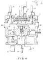
- Fig. 4 is a view showing one example of a plasma etching apparatus to which the present invention is applied.
- This apparatus comprises a processing chamber 11 whose inside is maintained to be substantially air-tight.
- the processing chamber 11 is formed of, for example aluminum the surface of which is anodized.
- the lower electrode 12 is formed of, for example, aluminum the surface of which is anodized.
- the lower electrode 12 there is formed a mounting section having a trapezoidal cross section in its central portion, and an object 15 to be processed, for example, a semiconductor wafer is mounted thereon.
- a surface portion of the electrode 12 except for the portion where the object is mounted is preferably coated with an insulating material, such as Teflon (trade name). Due to the coating, there can be improved a focus effect in which discharging concentrates on the object 15.
- the lower electrode 12 can be lifted by a lifter 13 with a maximum stroke of, for example, 30 mm.
- the airtight in the chamber 11 during lifting the lower electrode 12 is ensured by a bellows 14 made of, for example, stainless steel.
- a space 12a is formed in its central portion.
- a plurality of through holes (for example, four) which are through upward from the space 12a, and a lifter pin 16 made of, for example, stainless steel is inserted into each through hole.
- the lifter pin 16 is connected to a lift mechanism 18 via a plate 17.
- the lifter pin 16 is lifted by the drive of a lift mechanism 18.
- the lifter pin 16 moves up, so that the object 15 is separated from the lower electrode 12 to be in a transferable state.
- the lifter pin 16 moves down, so that the object 15 is mounted on the lower electrode 12.
- the lower electrode 12 and the plate 17 are connected to each other by a coil spring 19.
- a clamp ring 20 is provided above the lower electrode 12.
- the clamp ring 20 is used for uniformly pressing the object 15 to the surface of the lower electrode 12, and fixing the object 15 thereto.
- the central portion of the clamp ring 20 is shaped to correspond to the mounting portion of the lower electrode 12.
- the clamp ring 20 is formed of material having no influence on plasma, for example aluminum, the surface of which is anodized, quartz, and ceramic material such as alumina.
- the clamp ring 20 is held by a plurality of shafts 21 (for example four) which are airtightly through the upper portion of the chamber 11.
- Each shaft is connected to an independent driving mechanism such as an air cylinder 22, and each shaft moves up and down by the corresponding driving mechanism.
- the lower electrode 12 is moved up in a state that the object 15 is mounted on the lower electrode 12.
- the object 15 is brought into contact with the clamp ring 20. Moreover, the lower electrode 12 is moved up, so that the clamp ring 20 clamps the object 15 by pressing force of the air cylinder 22. While necessary pressing force is maintained the clamp ring 20 can be further moved up to a predetermined height, for example, by 5 mm by adjusting the drive of the air cylinder 22.
- a conductive material 23 is provided at the top portion of the chamber 11.
- the conductive material 23 is formed of, for example aluminum, the surface of which is anodized.
- An upper electrode 24, which is electrically connected to the conductive material 23, is provided away from the conductive material 23 with a narrow space 25.
- the upper electrode 24 is formed of, for example, amorphous carbon, aluminum, or aluminum the surface of which is anodized.
- a gas supply pipe 26 communicates with a space 25.
- the gas supply pipe 26 introduces processing gas from a gas supply source (not shown), which is arranged in the outside of the chamber 11, together with carrier gas.
- processing gas at least one of a gas containing oxygen or nitrogen is added to the HBr and HCl gases.
- oxygen or nitrogen may be added to the HBr and HCl gases after etching advances up to the portion near the SiO 2 layer.
- baffles 27 In the space 25, there are formed a plurality of baffles 27 having a plurality of openings in order to uniformly diffuse gas.
- a plurality of holes 28 is formed in the upper electrode 24 in order to supply gas diffused by baffles 27 into the chamber 11.
- a high frequency power supply 30 is connected to the upper electrode 24 via a capacitor 31 and the conductive material 23, and the lower electrode 12 is earthed. High frequency power is supplied to these electrodes from the power supply 30, so that plasma of processing gas generates between the electrodes.
- a plasma mode is a mode in which a radical etching is performed.
- the high voltage electrode is used as the lower electrode 12 and the upper electrode 24 is earthed, so that the mode can be in a reactant ion etching (RIE) mode.
- RIE reactant ion etching
- RF electric power whose phase differs at 180 degrees can be supplied between the upper electrode 24 and the lower electrode 12.
- magnetron etching type in which magnet is provided above or around the chamber 11, a crossed electromagnetic field is formed between the electrodes, and etching is performed. By use of magnet, etching treatment can be performed under a low pressure condition with high efficiency.
- a gas exhaust port 35 is formed in the lower side portion of the chamber 11, and the chamber 11 is exhausted from the gas exhaust port 35 by a vacuum pump (not shown).
- an inlet 32 for carrying in the object to be processed and an outlet 33 for carrying out the object are provided.
- load lock chambers 41 and 42 for carrying in and out are formed to be continuous to the inlet 32 and the outlet 33.
- These load lock chambers 41 and 42 have inlet and outlet side gates, respectively, and are able to be exhausted.
- one object to be processed is taken up by a sender (not shown) and inserted into the load lock chamber 41 for carrying in.
- the inlet side gate of the load lock chamber 41 is closed, and the inside thereof is exhausted.
- the outlet side gate is opened, and the object 15 is carried in the portion above the lower electrode 12 by a carrying-in mechanism (not shown).
- the lifter pin 16 is moved up and the object 15 is received at the top end of the lifter pin 16, and the carrying-in mechanism is retracted. Thereafter, the inside of the chamber 11 is made airtight.
- the lifter pin 16 is moved down, so that the object 15 is mounted on the lower electrode 12.
- the lower electrode 12 is moved up, and the surroundings of the object 15 is brought into contact with the clamp ring 20, and the object 15 is fixed to the clamp ring 20.
- the inside of the chamber 11 is exhausted, processing gas is introduced therein via the gas supply pipe 26 from the gas supply source, and the inside of the chamber is made to have a predetermined pressure, for example, 133.3 Pa (1 Torr) or less.
- the lower electrode 12 After etching, as the inside of the chamber 11 is exhausted, the lower electrode 12 is moved down and the lifter pin 16 is moved up, and the object 15 is mounted thereon. Then, the object 15 is carried out via the load lock chamber 42 for carrying out by an carrying-out mechanism (not shown).
- Example 1 explains the case in which a semiconductor wafer is used as a object to be processed, and a polysilicon layer thereof is etched.
- the above-mentioned etching apparatus was used, and HCl of 200 SCCM and HBr of 30 SCCM, both serving as processing gas, were introduced to the chamber.
- the pressure of the inside of the chamber was set to be 6.66 Pa (50m Torr), and high frequency electric power of 225W was supplied between the electrodes from high frequency power supply of 13. 56 MHz, and a polysilicon layer (having a thickness of 300 nm (3000 ⁇ )) of the semiconductor wafer was etched.
- the distance between the electrodes was set to be 0.6 cm.
- the etching treatment was made during the time in which the polysilicon layer was all etched in view of the calculation. Thereafter, oxygen or nitrogen containing gas such as O 2 , CO 2 , N 2 O were added to a processing gas at the various flow rates, respectively. An over-etching was performed for 60 min. under the same condition, and a residual portion of the polysilicon layer was removed. For comparison, there was an experiment in which oxygen or nitrogen containing gas is not added in over-etching, and the experimental result was shown in Table 1.
- the flow rate of oxygen or nitrogen containing gas was set to be 1, 3, 5, 10, and 15 SCCM.
- the etching rate of the base SiO 2 layer was 12,0 nm/min in the case in which O 2 , CO 2 , and N 2 O gases were not added.
- the etching rate of the SiO 2 layer was reduced to 8,0 to 5,4 nm/min even if the flow rate was 1 SCCM.
- the etching rate of the SiO 2 layer was considerably reduced when these rates were 3 SCCM or more, and the etching rate of the SiO 2 layer was 0 when the rate was 5 SCCM in the case of O 2 , N 2 O.
- these flow rates were 10 SCCM or more in the case of all gases, the etching rate of the SiO 2 layer was 0.
- the etching rate of the polysilicon layer was about 250 nm/min.
- the selection ratio of silicon to the base SiO 2 layer increased by these additive gases. Particularly, by adding gases at the rate of 3 SCCM or more, the selection rate of about 50 was increased to 100 to infinity.
- the etching shape was slightly deteriorated when the additive gas was 15 SCCM.
- the flow rate of additive gas was favorably 3 to 10 SCCM.
- the flow rate corresponds to the flow rate ratio of 1.3 to 4.2% to the flow rate of the processing gas.
- a curve A is a resist etching rate
- a curve B is an etching rate of the SiO 2 layer
- a curve C is an etching rate of the polysilicon layer.
- a curve D is a selection ratio of the polysilicon layer to the SiO 2 layer
- a curve E is a selection ratio of the polysilicon to the resist layer
- a curve F is uniformity of the polysilicon layer.
- HCl gas of 200 SCCM and HBr gas of 20 to 40 SCCM were favorably added in order to obtain a favorable etching having a high etching rate of polysilicon and a high selection ratio of the polysilicon layer to SiO 2 .
- the present invention relates to the etching method of the silicon containing layer, and the etching method is not limited to the plasma etching using the opposing electrodes. It is needless to say that the other method in which, for example, an ECR is used, may be employed.
Landscapes
- Drying Of Semiconductors (AREA)
Description
- The present invention relates to an etching method for a silicon containing layer of an object having a SiO2 film and a silicon containing layer adjacent thereto. This invention is applied, for example, to a case when a polysilicon layer, which is adjacent to the SiO2 film in a semiconductor wafer, is etched.
- US-4502915 describes a two-step plasma process for selective and isotropic etching of polycrystalline silicon. In the described process, the silicon is initially etched with a non-selective plasma etching gas in the first step until the first layer, which may contain contaminants is removed, and is then further etched in the second step, wherein selective plasma etching is performed by using hydrogen chloride and hydrogen bromide diluted with helium as the etching gas.
- EP 474 244 (prior art under Art 54(3) EPC) discloses a plasma processing method, wherein the plasma generation gas consists of hydrogen bromide or a gas mixture comprising hydrogen bromide, and may further contain hydrogen chloride, oxygen, chlorine and/or sulfur hexafluoride. The hydrogen bromide or the hydrogen bromide gas mixture can be diluted with helium or similar gases. The method described in EP 474 244 is said to be applicable to numerous silicon-containing films formed on a silicon oxide or nitride film, provided on a semiconductive substrate with high selectivity.
- A dry etching of polysilicon has been used in for example a MOS transistor. As shown in Fig. 1, a MOS semiconductor wafer is formed of a
silicon substrate 1, a SiO2gate insulating film 2 having a thickness of 10,0 to 30,0 nm formed on thesilicon substrate 1, apolysilicon layer 3 having a thickness of about 300 nm (3000 Å) formed on thegate insulating film 2, and aresist film 4 formed on thepolysilicon layer 3. In etching thepolysilicon layer 3 in such a semiconductor wafer, a mixture of HBr gas and Cℓ2 gas or HCℓ gas is used. - However, as shown in Fig. 2, in a portion where the
polysilicon layer 3 is step-like formed, a portion 3a whose thickness is larger than the other portions is provided since a wire layer is further formed on awire layer 7. As a result, in a case where the portion 3a and aportion 3b having a normal thickness are etched to be removed, theportion 3b is first removed by etching. As a result, as shown in Fig. 3, aresidual portion 5 is generated at a portion corresponding to the portion 3a. Then, if theresidual portion 5 is completely removed, thegate insulating film 2 is etched and a removal portion 6 shown in Fig. 3 may be formed. In other words, the part of thegate insulating film 2 is undesirably removed. - Since it is necessary to suppress damage of the Si substrate in etching polysilicon in the MOS semiconductor wafer, it is unfavorable that the above removed portion is formed. Therefore, it is required that the polysilicon layer be etched so as to have a high selection ratio to the SiO2 gate insulating film, that is, (etching speed of polysilicon)/(etching speed of SiO2). If the selection ratio is sufficiently high, the removal portion 6 can be considerably made small, and etching can be performed with a high accuracy of size.
- However, in the conventional polysilicon etching, the selection ratio is about 30 and this is insufficient for the accuracy of size.
- The present invention has been made in consideration of the above-mentioned problem, and an object of the invention is to provide a method for etching a silicon containing layer wherein the silicon containing layer can be etched at a high selection ratio to the SiO2 layer in an object to be processed in which the silicon containing layer such as a polysilicon layer is formed on the SiO2 layer.
- According to the present invention there is provided a method for etching a silicon containing layer in an object to be processed having a SiO2 film and a silicon containing layer which is adjacent to the SiO2 film and which is formed of silicon-containing material other than SiO2, comprising the steps of generating a plasma of a processing gas containing HBr and HCℓ gases, and selectively exposing a predetermined portion of the silicon containing layer in the plasma, thereby etching the portion, wherein the processing gas also includes at least one gas containing oxygen or nitrogen, with the proviso that the method does not comprise a step of irradiating the gas in the plasma generation area with light of a wavelength of not more than 436 nm, prior to the plasma generation.
- This invention can be more fully understood from the following detailed description when taken in conjunction with the accompanying drawings, in which:
- Fig. 1 is a cross sectional view showing a portion where a polysilicon layer in a semiconductor wafer is to be etched;
- Fig. 2 is a cross sectional view showing the portion where the polysilicon layer in the semiconductor wafer is to be etched and the polysilicon layer is step-like formed;
- Fig. 3 is a cross sectional view showing a state that the polysilicon layer of Fig. 2 is etched;
- Fig. 4 is a cross sectional view showing one example of the apparatuses executing the present invention;
- Fig. 5 is a schematic view showing a state that load lock chambers for carrying in and out are provided in the apparatus of Fig. 4;
- Fig. 6 is a graph showing an etching rate of each of the polysilicon layer, SiO2 layer, and a resist layer, in a case where HCℓ and HBr gas are used as gas containing halogen element and HBr gas flow is changed;
- Fig. 7 is a graph showing a selection ratio of the polysilicon layer to the SiO2 layer, a selection ratio of the polysilicon layer to the resist layer, and a uniformity of the polysilicon layer, in a case where HCℓ and HBr gas are used as gas containing halogen element and HBr gas flow is changed;
- The inventors of the present invention studied variously in view of a processing gas in connection with a method for etching a silicon containing layer at a high selection ratio to a SiO2 layer. As a result, the inventors found out that the selection ratio was able to be considerably increased by adding a gas containing oxygen or nitrogen in processing gas. More particulary, in a case where SiO2 is dissociated by ion impact due to plasma, oxygen in a processing gas is recombined with dissociated Si. On the other hand, a thin SiN film is formed on the surface of the SiO2 layer by existence of nitrogen in a processing gas, thereby protecting the SiO2 layer. Therefore, etching of the SiO2 layer can be suppressed, and the silicon containing layer can be etched at a high selection ratio to the SiO2 layer by adding gas containing oxygen or nitrogen to a processing gas. The present invention has been made based on the above-mentioned findings of the inventors of the present invention.
- The present invention will be explained in detail.
- The present invention is applied to an object to be processed having a SiO2 film and a silicon containing layer which is adjacent to the SiO2 film and which is formed of silicon-containing material other than SiO2. As such an object to be processed, a semiconductor wafer in which a polysilicon film is formed on the SiO2 film serving as an insulating film can be used. As a silicon containing layer, silicide such as WSi and silicon nitride can be used other than polysilicon.
- In plasma-etching the silicon containing layer of such an object to be processed, there is used at least one of a gas containing oxygen or nitrogen together with HCℓ and HBr gases as processing gas. The etching is performed by following procedures. The object to be processed is provided in a processing chamber. The inside of the treating chamber is depressurized. A treating gas is supplied therein. Plasma of processing gas is formed in the chamber. A predetermined portion of the silicon containing layer of the object is selectively exposed in plasma.
- The mixed gas of HCℓ and HBr is favorable and the flow rate thereof is 10 : 1 to 2 : 1 is preferable.
- A gas containing oxygen or nitrogen is not limited as long as oxygen or nitrogen is contained. However, O2, N2O, CO2, CO, N2, and NO2 is preferable.
- the ratio of the flow rate of a gas containing oxygen or nitrogen to that of the processing gas is preferably 10% or less. If this type of gas is slightly contained, the above-mentioned effect can be expected. However, if the flow rate ratio exceeds 10%, the etching speed decreases. The favorable flow rate ratio ranges from 1 to 4.5%.
- The pressure in the processing chamber while etching process is preferably 133.3 Pa (1 Torr) or less.
- In a case where the plasma-etching is performed as mentioned above, gas containing oxygen or nitrogen may be added in the treated gas from the beginning. However, during predetermined time in which there is not possibility of removal of SiO2 layer, only HCℓ and HBr gases are supplied and etching is performed. Oxygen or nitrogen is added to the processing gas after etching advances close to the SiO2 layer.
- The following explains an apparatus for executing the above-mentioned method.
- Fig. 4 is a view showing one example of a plasma etching apparatus to which the present invention is applied. This apparatus comprises a
processing chamber 11 whose inside is maintained to be substantially air-tight. Theprocessing chamber 11 is formed of, for example aluminum the surface of which is anodized. - In the lower portion of the
processing chamber 11, alower electrode 12 is provided. Thelower electrode 12 is formed of, for example, aluminum the surface of which is anodized. - In the
lower electrode 12, there is formed a mounting section having a trapezoidal cross section in its central portion, and anobject 15 to be processed, for example, a semiconductor wafer is mounted thereon. A surface portion of theelectrode 12 except for the portion where the object is mounted is preferably coated with an insulating material, such as Teflon (trade name). Due to the coating, there can be improved a focus effect in which discharging concentrates on theobject 15. - The
lower electrode 12 can be lifted by alifter 13 with a maximum stroke of, for example, 30 mm. The airtight in thechamber 11 during lifting thelower electrode 12 is ensured by abellows 14 made of, for example, stainless steel. - In the
lower electrode 12, a space 12a is formed in its central portion. A plurality of through holes (for example, four) which are through upward from the space 12a, and alifter pin 16 made of, for example, stainless steel is inserted into each through hole. Thelifter pin 16 is connected to alift mechanism 18 via aplate 17. Thelifter pin 16 is lifted by the drive of alift mechanism 18. Thelifter pin 16 moves up, so that theobject 15 is separated from thelower electrode 12 to be in a transferable state. Thelifter pin 16 moves down, so that theobject 15 is mounted on thelower electrode 12. In order to buffer the movement of thelifter pin 16, thelower electrode 12 and theplate 17 are connected to each other by acoil spring 19. - A
clamp ring 20 is provided above thelower electrode 12. Theclamp ring 20 is used for uniformly pressing theobject 15 to the surface of thelower electrode 12, and fixing theobject 15 thereto. The central portion of theclamp ring 20 is shaped to correspond to the mounting portion of thelower electrode 12. Theclamp ring 20 is formed of material having no influence on plasma, for example aluminum, the surface of which is anodized, quartz, and ceramic material such as alumina. Theclamp ring 20 is held by a plurality of shafts 21 (for example four) which are airtightly through the upper portion of thechamber 11. Each shaft is connected to an independent driving mechanism such as anair cylinder 22, and each shaft moves up and down by the corresponding driving mechanism. Thelower electrode 12 is moved up in a state that theobject 15 is mounted on thelower electrode 12. Due to this, theobject 15 is brought into contact with theclamp ring 20. Moreover, thelower electrode 12 is moved up, so that theclamp ring 20 clamps theobject 15 by pressing force of theair cylinder 22. While necessary pressing force is maintained theclamp ring 20 can be further moved up to a predetermined height, for example, by 5 mm by adjusting the drive of theair cylinder 22. - A
conductive material 23 is provided at the top portion of thechamber 11. Theconductive material 23 is formed of, for example aluminum, the surface of which is anodized. Anupper electrode 24, which is electrically connected to theconductive material 23, is provided away from theconductive material 23 with anarrow space 25. Theupper electrode 24 is formed of, for example, amorphous carbon, aluminum, or aluminum the surface of which is anodized. - A
gas supply pipe 26 communicates with aspace 25. Thegas supply pipe 26 introduces processing gas from a gas supply source (not shown), which is arranged in the outside of thechamber 11, together with carrier gas. As processing gas, at least one of a gas containing oxygen or nitrogen is added to the HBr and HCl gases. Moreover, oxygen or nitrogen may be added to the HBr and HCl gases after etching advances up to the portion near the SiO2 layer. - In the
space 25, there are formed a plurality ofbaffles 27 having a plurality of openings in order to uniformly diffuse gas. A plurality ofholes 28 is formed in theupper electrode 24 in order to supply gas diffused bybaffles 27 into thechamber 11. - Note that, a
shield ring 29, which is formed of insulating material such as Teflon, is provided in the peripheral portion of theupper electrode 24, and plasma can be generated to have the same diameter as theobject 15. - A high
frequency power supply 30 is connected to theupper electrode 24 via acapacitor 31 and theconductive material 23, and thelower electrode 12 is earthed. High frequency power is supplied to these electrodes from thepower supply 30, so that plasma of processing gas generates between the electrodes. In this case, a plasma mode is a mode in which a radical etching is performed. - The high voltage electrode is used as the
lower electrode 12 and theupper electrode 24 is earthed, so that the mode can be in a reactant ion etching (RIE) mode. Moreover, RF electric power whose phase differs at 180 degrees can be supplied between theupper electrode 24 and thelower electrode 12. Furthermore, there may be used a magnetron etching type in which magnet is provided above or around thechamber 11, a crossed electromagnetic field is formed between the electrodes, and etching is performed. By use of magnet, etching treatment can be performed under a low pressure condition with high efficiency. - A
gas exhaust port 35 is formed in the lower side portion of thechamber 11, and thechamber 11 is exhausted from thegas exhaust port 35 by a vacuum pump (not shown). - In the two side surfaces of the
chamber 11 opposing to each other, aninlet 32 for carrying in the object to be processed and anoutlet 33 for carrying out the object are provided. Moreover, as schematically shown in Fig. 5,load lock chambers inlet 32 and theoutlet 33. Theseload lock chambers load lock chambers chamber 11 come in contact with air. - In performing plasma etching by use of the above-mentioned apparatus, first of all, one object to be processed is taken up by a sender (not shown) and inserted into the
load lock chamber 41 for carrying in. The inlet side gate of theload lock chamber 41 is closed, and the inside thereof is exhausted. Thereafter, the outlet side gate is opened, and theobject 15 is carried in the portion above thelower electrode 12 by a carrying-in mechanism (not shown). Thelifter pin 16 is moved up and theobject 15 is received at the top end of thelifter pin 16, and the carrying-in mechanism is retracted. Thereafter, the inside of thechamber 11 is made airtight. Thelifter pin 16 is moved down, so that theobject 15 is mounted on thelower electrode 12. Then, thelower electrode 12 is moved up, and the surroundings of theobject 15 is brought into contact with theclamp ring 20, and theobject 15 is fixed to theclamp ring 20. - The inside of the
chamber 11 is exhausted, processing gas is introduced therein via thegas supply pipe 26 from the gas supply source, and the inside of the chamber is made to have a predetermined pressure, for example, 133.3 Pa (1 Torr) or less. - Thereafter, RF electric power is supplied between the
upper electrode 24 and thelower electrode 12, and plasma of processing gas is generated therebetween. By means of the plasma, the silicon containing layer of theobject 15 is etched. - After etching, as the inside of the
chamber 11 is exhausted, thelower electrode 12 is moved down and thelifter pin 16 is moved up, and theobject 15 is mounted thereon. Then, theobject 15 is carried out via theload lock chamber 42 for carrying out by an carrying-out mechanism (not shown). - An Example of the present invention will be explained as follows.
- Example 1 explains the case in which a semiconductor wafer is used as a object to be processed, and a polysilicon layer thereof is etched.
- In this Example, the above-mentioned etching apparatus was used, and HCℓ of 200 SCCM and HBr of 30 SCCM, both serving as processing gas, were introduced to the chamber. The pressure of the inside of the chamber was set to be 6.66 Pa (50m Torr), and high frequency electric power of 225W was supplied between the electrodes from high frequency power supply of 13. 56 MHz, and a polysilicon layer (having a thickness of 300 nm (3000 Å)) of the semiconductor wafer was etched. The distance between the electrodes was set to be 0.6 cm.
- The etching treatment was made during the time in which the polysilicon layer was all etched in view of the calculation. Thereafter, oxygen or nitrogen containing gas such as O2, CO2, N2O were added to a processing gas at the various flow rates, respectively. An over-etching was performed for 60 min. under the same condition, and a residual portion of the polysilicon layer was removed. For comparison, there was an experiment in which oxygen or nitrogen containing gas is not added in over-etching, and the experimental result was shown in Table 1. The flow rate of oxygen or nitrogen containing gas was set to be 1, 3, 5, 10, and 15 SCCM.
Table 1 Gas Flow Rate O2 CO2 N2O 0 SCCM 12,0 nm/ min 12,0 nm/ min 12,0 nm/ min 1 SCCM 8,0 nm/ min 7,7 nm/ min 5,4 nm/ min 3 SCCM 0,8 nm/min - - 5 SCCM 0 nm/ min 2,7 nm/ min 0 nm/ min 10 SCCM 0 nm/ min 0 nm/ min 0 nm/ min 15 SCCM 0 nm/ min 0 nm/ min 0 nm/min - As shown in Table 1, the etching rate of the base SiO2 layer was 12,0 nm/min in the case in which O2, CO2, and N2O gases were not added. In contrast, in the case in which O2, CO2, and N2O gases were added, the etching rate of the SiO2 layer was reduced to 8,0 to 5,4 nm/min even if the flow rate was 1 SCCM. Particularly, the etching rate of the SiO2 layer was considerably reduced when these rates were 3 SCCM or more, and the etching rate of the SiO2 layer was 0 when the rate was 5 SCCM in the case of O2, N2O. When these flow rates were 10 SCCM or more in the case of all gases, the etching rate of the SiO2 layer was 0.
- In this case, the etching rate of the polysilicon layer was about 250 nm/min.
- As a result, the following fact was confirmed.
- The selection ratio of silicon to the base SiO2 layer increased by these additive gases. Particularly, by adding gases at the rate of 3 SCCM or more, the selection rate of about 50 was increased to 100 to infinity.
- Moreover, there was a tendency that the etching shape was slightly deteriorated when the additive gas was 15 SCCM. In view of this point, it was confirmed that the flow rate of additive gas was favorably 3 to 10 SCCM. The flow rate corresponds to the flow rate ratio of 1.3 to 4.2% to the flow rate of the processing gas.
- The above result shows the case in which O2, CO2, N2O were individually added. In the case in which these gases were mixed and the total amount was set as Table 1, substantially the same result as Table 1 was obtained.
- Next, an experiment on influence of the flow rate ratio on the etching was conducted in the case in which HCℓ and HBr gases both serving as halogen element containing gases were used.
- In this case, the flow rate of HCℓ gas was set to 200 SCCM, and the flow rate of HBr gas was changed in the rate of 15 to 50 SCCM. Then, the etching was performed in a state that the pressure of the inside of the chamber was set to 80 Pa (600m Torr), high frequency electric power was 250 W, and the temperature was 20°C. The result was shown in Figs. 6 and 7. In Fig. 6, a curve A is a resist etching rate, a curve B is an etching rate of the SiO2 layer, and a curve C is an etching rate of the polysilicon layer. In Fig. 7, a curve D is a selection ratio of the polysilicon layer to the SiO2 layer, a curve E is a selection ratio of the polysilicon to the resist layer, and a curve F is uniformity of the polysilicon layer.
- As shown in these figures, it was confirmed that HCℓ gas of 200 SCCM and HBr gas of 20 to 40 SCCM were favorably added in order to obtain a favorable etching having a high etching rate of polysilicon and a high selection ratio of the polysilicon layer to SiO2.
- The present invention relates to the etching method of the silicon containing layer, and the etching method is not limited to the plasma etching using the opposing electrodes. It is needless to say that the other method in which, for example, an ECR is used, may be employed.
Claims (16)
- A method for etching a silicon containing layer in an object to be processed having a SiO2 film and a silicon containing layer which is adjacent to the SiO2 film and which is formed of silicon-containing material other than SiO2, comprising the steps of:generating a plasma of a processing gas containing HBr gas, HCl gas and at least one oxygen-containing gas or nitrogen-containing gas; andselectively exposing a predetermined portion of the silicon containing layer in the plasma, thereby etching said portion, with the proviso that the method does not comprise a step of irradiating the gas in the plasma generation area with light of a wavelength of not more than 436 nm, prior to the plasma generation.
- The method according to claim 1, characterized in that said gas containing oxygen or nitrogen is at least one selected from a group consisting of O2 gas, N2O gas, CO2 gas, CO gas, N2 gas, and NO2 gas.
- The method according to claim 1, characterized in that a flow rate ratio of HCl gas and HBr gas is 10:1 to 2:1.
- The method according to claim 1, characterized in that a ratio of a flow rate of said gas containing oxygen or nitrogen to that of said processing gas is 10% or less.
- The method according to claim 4, characterized in that the ratio of the flow rate of said gas containing oxygen or nitrogen to that of said processing gas is 1 to 4.5%.
- The method according to claim 1, characterized in that the plasma of said processing gas is generated by supplying said processing gas to a chamber where said object to be processed is inserted, and by supplying high frequency electric power between a pair of electrodes opposing to each other.
- The method according to claim 6 characterized in that the pressure in the chamber is set to 133.3 Pa (1 Torr) or less when the plasma is generated.
- The method according to claim 1, characterized in that said silicon containing layer is a polysilicon layer.
- A method for etching a silicon containing layer in an object to be processed having a SiO2 film and a silicon containing layer which is adjacent to the SiO2 film and which is formed of silicon-containing material other than SiO2, comprising the steps of:generating a plasma of a processing gas containing HBr gas and HCl gas;selectively exposing a predetermined portion of the silicon containing layer in the plasma thereby etching said portion;adding at least one gas containing oxygen or nitrogen to the processing gas at the time when said silicon containing layer is etched to a predetermined thickness by plasma; andetching a residual portion of said silicon containing layer by plasma of the processing gas in which said gas containing oxygen or nitrogen is added.
- The method according to claim 9, characterized in that said gas containing oxygen or nitrogen is at least one selected from a group consisting of O2 gas, N2O gas, CO2 gas, CO gas, N2 gas, and NO2 gas.
- The method according to claim 9, characterized in that a flow rate ratio of HCl gas and HBr gas is 10:1 to 2:1.
- The method according to claim 9, characterized in that a ratio of a flow rate of said gas containing oxygen or nitrogen to that of said processing gas is 10% or less.
- The method according to claim 12, characterized in that the ratio of the flow rate of said gas containing oxygen or nitrogen to that of said processing gas is 1 to 4.5%.
- The method according to claim 9, characterized in that the plasma of said processing gas is generated by supplying said processing gas to a chamber where the said object to be processed is inserted, and by supplying high frequency electric power between a pair of electrodes opposing to each other.
- The method according to claim 14, characterized in that the pressure in the chamber is set to 133 Pa (1 Torr) or less when the plasma is generated.
- The method according to claim 9, characterized in that said silicon containing layer is a polysilicon layer.
Applications Claiming Priority (2)
| Application Number | Priority Date | Filing Date | Title |
|---|---|---|---|
| JP78317/91 | 1991-03-19 | ||
| JP3078317A JP2920848B2 (en) | 1991-03-19 | 1991-03-19 | Silicon layer etching method |
Publications (3)
| Publication Number | Publication Date |
|---|---|
| EP0504758A2 EP0504758A2 (en) | 1992-09-23 |
| EP0504758A3 EP0504758A3 (en) | 1993-06-09 |
| EP0504758B1 true EP0504758B1 (en) | 1997-06-18 |
Family
ID=13658565
Family Applications (1)
| Application Number | Title | Priority Date | Filing Date |
|---|---|---|---|
| EP92104397A Expired - Lifetime EP0504758B1 (en) | 1991-03-19 | 1992-03-13 | Plasma etching method for silicon containing layer |
Country Status (5)
| Country | Link |
|---|---|
| EP (1) | EP0504758B1 (en) |
| JP (1) | JP2920848B2 (en) |
| KR (1) | KR0175073B1 (en) |
| DE (1) | DE69220398T2 (en) |
| TW (1) | TW201847B (en) |
Families Citing this family (5)
| Publication number | Priority date | Publication date | Assignee | Title |
|---|---|---|---|---|
| US6165375A (en) * | 1997-09-23 | 2000-12-26 | Cypress Semiconductor Corporation | Plasma etching method |
| TW455948B (en) * | 1999-09-13 | 2001-09-21 | Motorola Inc | Process for etching an insulating layer and forming a semiconductor device |
| US6794294B1 (en) * | 1999-11-09 | 2004-09-21 | Koninklijke Philips Electronics N.V. | Etch process that resists notching at electrode bottom |
| US8679982B2 (en) * | 2011-08-26 | 2014-03-25 | Applied Materials, Inc. | Selective suppression of dry-etch rate of materials containing both silicon and oxygen |
| JP7178918B2 (en) * | 2019-01-30 | 2022-11-28 | 東京エレクトロン株式会社 | Etching method, plasma processing apparatus, and processing system |
Family Cites Families (7)
| Publication number | Priority date | Publication date | Assignee | Title |
|---|---|---|---|---|
| US4431477A (en) * | 1983-07-05 | 1984-02-14 | Matheson Gas Products, Inc. | Plasma etching with nitrous oxide and fluoro compound gas mixture |
| US4502915B1 (en) * | 1984-01-23 | 1998-11-03 | Texas Instruments Inc | Two-step plasma process for selective anisotropic etching of polycrystalline silicon without leaving residue |
| US4726879A (en) * | 1986-09-08 | 1988-02-23 | International Business Machines Corporation | RIE process for etching silicon isolation trenches and polycides with vertical surfaces |
| EP0272143B1 (en) * | 1986-12-19 | 1999-03-17 | Applied Materials, Inc. | Bromine etch process for silicon |
| DE68928977T2 (en) * | 1988-02-09 | 1999-08-19 | Fujitsu Ltd. | Dry etching with hydrogen bromide or bromine |
| US5007982A (en) * | 1988-07-11 | 1991-04-16 | North American Philips Corporation | Reactive ion etching of silicon with hydrogen bromide |
| JP3004699B2 (en) * | 1990-09-07 | 2000-01-31 | 東京エレクトロン株式会社 | Plasma processing method |
-
1991
- 1991-03-19 JP JP3078317A patent/JP2920848B2/en not_active Expired - Fee Related
-
1992
- 1992-03-12 TW TW081101894A patent/TW201847B/zh active
- 1992-03-13 DE DE69220398T patent/DE69220398T2/en not_active Expired - Fee Related
- 1992-03-13 EP EP92104397A patent/EP0504758B1/en not_active Expired - Lifetime
- 1992-03-18 KR KR1019920004453A patent/KR0175073B1/en not_active Expired - Fee Related
Also Published As
| Publication number | Publication date |
|---|---|
| TW201847B (en) | 1993-03-11 |
| DE69220398D1 (en) | 1997-07-24 |
| EP0504758A2 (en) | 1992-09-23 |
| JPH04290430A (en) | 1992-10-15 |
| JP2920848B2 (en) | 1999-07-19 |
| KR920018858A (en) | 1992-10-22 |
| DE69220398T2 (en) | 1997-11-06 |
| EP0504758A3 (en) | 1993-06-09 |
| KR0175073B1 (en) | 1999-04-01 |
Similar Documents
| Publication | Publication Date | Title |
|---|---|---|
| JP5419354B2 (en) | Multilayer high quality gate dielectric for low temperature polysilicon TFTs | |
| KR100639147B1 (en) | Plasma processing method | |
| EP0776032B1 (en) | Plasma etching method | |
| US7955510B2 (en) | Oxide etch with NH4-NF3 chemistry | |
| US6902681B2 (en) | Method for plasma etching of high-K dielectric materials | |
| US20060252265A1 (en) | Etching high-kappa dielectric materials with good high-kappa foot control and silicon recess control | |
| US20020036066A1 (en) | Method and apparatus for processing substrates | |
| US20230260802A1 (en) | Highly selective silicon etching | |
| EP1840946A1 (en) | Method for cleaning of semiconductor processing apparatus and method for ethching silicon substrate | |
| JPH06188229A (en) | Post-etching method | |
| US6855643B2 (en) | Method for fabricating a gate structure | |
| US12374557B2 (en) | Methods for etching structures with oxygen pulsing | |
| CN114639602B (en) | Etching methods and etching apparatus | |
| US5560804A (en) | Etching method for silicon containing layer | |
| KR20210110734A (en) | Vertical Transistor Fabrication for Memory Applications | |
| JP3808902B2 (en) | Plasma etching method | |
| JP2005039015A (en) | Plasma processing method and apparatus | |
| JPH08115901A (en) | Plasma processing method and plasma processing apparatus | |
| KR100966927B1 (en) | Manufacturing Method of Insulating Film and Manufacturing Method of Semiconductor Device | |
| JPH11168090A (en) | Semiconductor manufacturing method | |
| EP0504758A2 (en) | Plasma etching method fo silicon containing layer | |
| JP2022094914A (en) | Etching method and etching device | |
| KR102931045B1 (en) | Etching method and etching apparatus | |
| JP3732079B2 (en) | Sample surface processing method | |
| JPH04364731A (en) | Etching method |
Legal Events
| Date | Code | Title | Description |
|---|---|---|---|
| PUAI | Public reference made under article 153(3) epc to a published international application that has entered the european phase |
Free format text: ORIGINAL CODE: 0009012 |
|
| 17P | Request for examination filed |
Effective date: 19920313 |
|
| AK | Designated contracting states |
Kind code of ref document: A2 Designated state(s): DE FR GB IT NL |
|
| PUAL | Search report despatched |
Free format text: ORIGINAL CODE: 0009013 |
|
| AK | Designated contracting states |
Kind code of ref document: A3 Designated state(s): DE FR GB IT NL |
|
| 17Q | First examination report despatched |
Effective date: 19931210 |
|
| GRAG | Despatch of communication of intention to grant |
Free format text: ORIGINAL CODE: EPIDOS AGRA |
|
| GRAH | Despatch of communication of intention to grant a patent |
Free format text: ORIGINAL CODE: EPIDOS IGRA |
|
| RAP1 | Party data changed (applicant data changed or rights of an application transferred) |
Owner name: TOKYO ELECTRON LIMITED |
|
| RAP1 | Party data changed (applicant data changed or rights of an application transferred) |
Owner name: TOKYO ELECTRON LIMITED |
|
| GRAH | Despatch of communication of intention to grant a patent |
Free format text: ORIGINAL CODE: EPIDOS IGRA |
|
| GRAA | (expected) grant |
Free format text: ORIGINAL CODE: 0009210 |
|
| RBV | Designated contracting states (corrected) |
Designated state(s): DE GB |
|
| AK | Designated contracting states |
Kind code of ref document: B1 Designated state(s): DE GB |
|
| REF | Corresponds to: |
Ref document number: 69220398 Country of ref document: DE Date of ref document: 19970724 |
|
| PLBE | No opposition filed within time limit |
Free format text: ORIGINAL CODE: 0009261 |
|
| STAA | Information on the status of an ep patent application or granted ep patent |
Free format text: STATUS: NO OPPOSITION FILED WITHIN TIME LIMIT |
|
| 26N | No opposition filed | ||
| REG | Reference to a national code |
Ref country code: GB Ref legal event code: IF02 |
|
| PGFP | Annual fee paid to national office [announced via postgrant information from national office to epo] |
Ref country code: GB Payment date: 20020313 Year of fee payment: 11 |
|
| PG25 | Lapsed in a contracting state [announced via postgrant information from national office to epo] |
Ref country code: GB Free format text: LAPSE BECAUSE OF NON-PAYMENT OF DUE FEES Effective date: 20030313 |
|
| GBPC | Gb: european patent ceased through non-payment of renewal fee |
Effective date: 20030313 |
|
| PGFP | Annual fee paid to national office [announced via postgrant information from national office to epo] |
Ref country code: DE Payment date: 20050310 Year of fee payment: 14 |
|
| PG25 | Lapsed in a contracting state [announced via postgrant information from national office to epo] |
Ref country code: DE Free format text: LAPSE BECAUSE OF NON-PAYMENT OF DUE FEES Effective date: 20061003 |