EP0501761B1 - Apparatus for lighting of liquid crystal display - Google Patents
Apparatus for lighting of liquid crystal display Download PDFInfo
- Publication number
- EP0501761B1 EP0501761B1 EP92301589A EP92301589A EP0501761B1 EP 0501761 B1 EP0501761 B1 EP 0501761B1 EP 92301589 A EP92301589 A EP 92301589A EP 92301589 A EP92301589 A EP 92301589A EP 0501761 B1 EP0501761 B1 EP 0501761B1
- Authority
- EP
- European Patent Office
- Prior art keywords
- light
- optical conductor
- liquid crystal
- incident end
- light incident
- Prior art date
- Legal status (The legal status is an assumption and is not a legal conclusion. Google has not performed a legal analysis and makes no representation as to the accuracy of the status listed.)
- Expired - Lifetime
Links
Images

Classifications
-
- G—PHYSICS
- G02—OPTICS
- G02B—OPTICAL ELEMENTS, SYSTEMS OR APPARATUS
- G02B6/00—Light guides; Structural details of arrangements comprising light guides and other optical elements, e.g. couplings
- G02B6/0001—Light guides; Structural details of arrangements comprising light guides and other optical elements, e.g. couplings specially adapted for lighting devices or systems
- G02B6/0011—Light guides; Structural details of arrangements comprising light guides and other optical elements, e.g. couplings specially adapted for lighting devices or systems the light guides being planar or of plate-like form
- G02B6/0033—Means for improving the coupling-out of light from the light guide
-
- G—PHYSICS
- G02—OPTICS
- G02B—OPTICAL ELEMENTS, SYSTEMS OR APPARATUS
- G02B6/00—Light guides; Structural details of arrangements comprising light guides and other optical elements, e.g. couplings
- G02B6/0001—Light guides; Structural details of arrangements comprising light guides and other optical elements, e.g. couplings specially adapted for lighting devices or systems
-
- G—PHYSICS
- G02—OPTICS
- G02B—OPTICAL ELEMENTS, SYSTEMS OR APPARATUS
- G02B6/00—Light guides; Structural details of arrangements comprising light guides and other optical elements, e.g. couplings
- G02B6/0001—Light guides; Structural details of arrangements comprising light guides and other optical elements, e.g. couplings specially adapted for lighting devices or systems
- G02B6/0011—Light guides; Structural details of arrangements comprising light guides and other optical elements, e.g. couplings specially adapted for lighting devices or systems the light guides being planar or of plate-like form
- G02B6/0033—Means for improving the coupling-out of light from the light guide
- G02B6/0058—Means for improving the coupling-out of light from the light guide varying in density, size, shape or depth along the light guide
- G02B6/0061—Means for improving the coupling-out of light from the light guide varying in density, size, shape or depth along the light guide to provide homogeneous light output intensity
Definitions
- the present invention relates to a lighting apparatus of edge light type used for backlighting of a light receiving type liquid crystal display device.
- a conventional lighting apparatus of edge light type used for a liquid crystal display device lamps such as cold cathode tubes or hot cathode tubes are used as light sources 1, the light sources 1 are disposed at opposite ends of an optical conductor 2, a diffusion sheet 3 for uniforming the brightness over the entire lighting surface, which is formed of a milk-white, synthetic resin plate using such as acryl, polycarbonate or polyester plate, is provided on the top surface of the optical conductor 2, and a mirror reflector plate or a light scattering acryl plate is used as a reflector sheet 4.
- the reflector sheet 4 is adapted to improve the utilization efficiency of light by reflecting light, emitted from the light sources and heading to the back side, toward the front side.
- EP-A-0 355 064 on which the preamble of claim 1 is based, also discloses a lighting apparatus for a liquid crystal display as hereinabove described.
- Fig.1 Denoted in Fig.1 by 7 is light source reflectors for reflecting, light emitted from the light sources and heading to the outside, toward the optical conductor 2 and by X is a liquid crystal display panel.
- the light propagates through the optical conductor 2 while repeating total reflection.
- an angle between light incident on a light outgoing surface 6 standing for the top surface of the optical conductor 2 and a normal vector of the light outgoing surface 6 is ⁇ o and the refractive index of the optical conductor 2 is n o
- the light can go out of the light outgoing surface 6 only when ⁇ o ⁇ sin ⁇ 1 (1/n o ) is valid.
- the light repeats total reflection in the optical conductor 2 to travel therethrough while undergoing a decrease in flux of light and a material absorption subject to an absorption coefficient ⁇ of an optical conductor material during propagation in the optical conductor 2.
- the present invention intends to eliminate the aforementioned problems and it is an object of the invention to provide a lighting apparatus which can reduce the decrease in flux of light and the material absorption in the optical conductor to have high utilization efficiency of light and high brightness.
- a liquid crystal lighting apparatus adapted to backlight a liquid crystal display panel
- the apparatus comprising an optical conductor adapted to be disposed in parallel with the liquid crystal display panel to be backlit and a light source disposed at an end of said optical conductor, wherein said optical conductor has a light incident end surface opposing said light source and a light outgoing surface opposing, in use, said liquid crystal display panel;
- the apparatus being characterized in that the optical conductor is constructed of a plurality of refractive layers sequentially laminated along optical paths of light from the light source and having different refractive indices, the refractive indices reducing in a direction away from said light incident end surface so that light incoming from said light incident end surface is refracted to make an incident angle at said light outgoing surface smaller than a critical angle.
- the optical conductor is constructed of the plurality of laminated refractive layers N1, N2, ..., N i having the different refractive indices, the light coming from the light incident end surfaces is refracted at interfaces at the boundaries of the refractive layers N1, N2, ..., N i to take an incident angle ⁇ i smaller than a critical angle ⁇ w when reaching the light outgoing surface, thereby ensuring that the light can be prevented from undergoing total reflection at the light outgoing surface and so the optical path length in the optical conductor can be shortened.
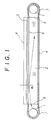
- Fig.1 is a longitudinal sectional view showing a prior art liquid crystal lighting apparatus.
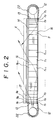
- Fig.2 is a longitudinal sectional view showing a liquid crystal lighting apparatus according to an embodiment of the invention.
- Fig.3 is a fragmentary, enlarged longitudinal sectional view showing light paths in the Fig.2 embodiment.
- FIG.2 An apparatus for lighting liquid crystal according to an embodiment of the invention is shown, in longitudinal sectional form, in Fig.2 and light paths in the embodiment are shown, in fragmentary, enlarged longitudinal sectional form, in Fig.3.
- the liquid crystal lighting apparatus of the present embodiment is an edge light type lighting apparatus adapted to backlight a liquid crystal panel X and it comprises an optical conductor 11 disposed in parallel with the liquid crystal display panel X, light sources 12 disposed at opposite ends of the optical conductor 11, a reflector sheet 16 for reflecting light, heading backwards in the optical conductor 11, toward the liquid crystal display panel X, and a diffusion sheet 17 for uniforming the brightness over the entire lighting surface.
- the optical conductor 11 has light incident end surfaces 13 opposing the light sources 12 and a light outgoing surface 14 opposing the liquid crystal display panel X and it is shaped into a flat plate of a thickness of 2 to 10mm.
- the light incident end surfaces 13 are orthogonal to the light outgoing surface 14.
- the optical conductor 11 has a dispersive type refractive index. More specifically, the optical conductor 11 is constructed of a plurality of refractive layers N1, N2,..., N i sequentially laminated along the optical path and having different refractive indices effective to refract light coming from the light incident end surfaces 13 so as to make an incident angle ⁇ i at the light outgoing surface 14 smaller than a critical angle ⁇ w .
- the individual refractive layers N1, N2, ..., N i are formed through molding process using transparent resin materials such as acryl, polycarbonate or polyester materials having refractive indices different from each other.
- the refractive indices n1, n2, ..., n i of the refractive layers N1, N2, ..., N i are so set as to be lowered gradually from the light incident end surfaces to a center portion of the optical conductor 11.
- Widths of the refractive layers N1, N2,..., N i are so set as to be gradually increased from the light incident end surfaces 13 to the center portion in order that the quantity of light at the light outgoing surface 14 is adjusted to have uniformity.
- the interface between adjacent ones of the refractive layers N1, N2, ..., N i is made to be vertical to the light outgoing surface 14.
- the light source 12 Used as the light source 12 is a hot cathode tube of linear tube type consisting of a luminous element such as a filament and envelope enclosing the element.
- the light source 12 has a diameter of 3 to 8mm and an effective lamp length of 100 to 220mm.
- Used as the reflector sheet 16 is an existing mirror surface reflector, light scattering acryl plate or the like.
- the diffusion sheet 17 is a milk-white synthetic resin plate having a thickness of 0.07 to 0.3mm and a transmittivity of 87 to 93 % for visual rays of 600nm wavelength.
- synthetic resin known materials such as polycarbonate and polyester may selectively be used as desired.
- reference numeral 22 designates light source reflectors for reflecting light, emitted from the light sources 12 and heading in directions opposite to the optical conductor 11, toward the optical conductor 11.
- the light travelling in the optical conductor is distributed to the diffusion sheet 17 through the light outgoing surface 14.
- the light is then distributed substantially uniformly by means of the diffusion sheet 17 to backlight the liquid crystal display panel X.
- the optical conductor 11 is constructed of the plurality of laminated refractive layers N1, N2, ..., N i of different refractive indices which are so set as to be gradually lowered from the light incident end surfaces 13 to the center portion of the optical conductor 11 and therefore, the light entering the light incident end surface 13 undergoes increasing angles of refraction ⁇ 1, ⁇ 2, ⁇ 3, ⁇ 4, ... at interface between adjacent ones of the refractive layers N1, N2, ... N i as it proceeds to the center portion of the optical conductor 11, as shown in Fig.3.
- the angle of refraction ⁇ i can be increased to ensure that the light travelling in the optical conductor 11 can be so guided as not to undergo total reflection.
- all of the light beams can go out of the light outgoing surface 14 as they reach it for the first time and so the optical path in the optical conductor 11 can be shortened. Therefore, a decrease in flux of light at the reflector surface of the optical conductor 11 and a decrease in light flux due to absorption by the material can be mitigated drastically and the surface brightness of the liquid crystal lighting apparatus can be improved.
- a light source may be provided only at one end.
- the optical conductor is constructed of the plurality of laminated refractive layers, light coming from the light incident end surfaces can be refracted at the interfaces of the refractive layers to make the incident angle the outgoing light takes at the light outgoing surface smaller than the critical angle.
Landscapes
- Physics & Mathematics (AREA)
- General Physics & Mathematics (AREA)
- Optics & Photonics (AREA)
- Liquid Crystal (AREA)
- Planar Illumination Modules (AREA)
- Light Guides In General And Applications Therefor (AREA)
Description
- The present invention relates to a lighting apparatus of edge light type used for backlighting of a light receiving type liquid crystal display device.
- Conventionally, many examples of lighting apparatus for liquid crystal display devices have been disclosed in such Japanese Laid-open patent publications as Nos. 987/1989 and 171009/1991. In general, as shown in Fig. 1, in a conventional lighting apparatus of edge light type used for a liquid crystal display device, lamps such as cold cathode tubes or hot cathode tubes are used as
light sources 1, thelight sources 1 are disposed at opposite ends of anoptical conductor 2, adiffusion sheet 3 for uniforming the brightness over the entire lighting surface, which is formed of a milk-white, synthetic resin plate using such as acryl, polycarbonate or polyester plate, is provided on the top surface of theoptical conductor 2, and a mirror reflector plate or a light scattering acryl plate is used as areflector sheet 4. Thereflector sheet 4 is adapted to improve the utilization efficiency of light by reflecting light, emitted from the light sources and heading to the back side, toward the front side. - EP-A-0 355 064, on which the preamble of
claim 1 is based, also discloses a lighting apparatus for a liquid crystal display as hereinabove described. - Especially, in the field of colour LCD panels, it is indispensable to employ stacked polarizer plates which utilize optical anisotropy of liquid crystal and the polarizer plates will cut illumination light by about 50 %; and therefore, a backlighting system of higher brightness is needed and it is of importance to improve the utilization efficiency of light.
- Denoted in Fig.1 by 7 is light source reflectors for reflecting, light emitted from the light sources and heading to the outside, toward the
optical conductor 2 and by X is a liquid crystal display panel. - In the conventional liquid crystal lighting apparatus of edge light type wherein light is introduced from light
incident end surfaces 5 at the opposite ends of theoptical conductor 2, the light propagates through theoptical conductor 2 while repeating total reflection. In case where an angle between light incident on a lightoutgoing surface 6 standing for the top surface of theoptical conductor 2 and a normal vector of the lightoutgoing surface 6 is ϑo and the refractive index of theoptical conductor 2 is no, the light can go out of the lightoutgoing surface 6 only when

optical conductor 2 to travel therethrough while undergoing a decrease in flux of light and a material absorption subject to an absorption coefficient α of an optical conductor material during propagation in theoptical conductor 2. More particularly, where an optical path length through which light travels before reaching the light outgoing surface is P and a lamp light flux value at the light incident end surface of the optical conductor is Fo, the light undergoes an decrease in flux of light pursuant to
- The present invention intends to eliminate the aforementioned problems and it is an object of the invention to provide a lighting apparatus which can reduce the decrease in flux of light and the material absorption in the optical conductor to have high utilization efficiency of light and high brightness.
- According to the present invention there is provided a liquid crystal lighting apparatus adapted to backlight a liquid crystal display panel, the apparatus comprising an optical conductor adapted to be disposed in parallel with the liquid crystal display panel to be backlit and a light source disposed at an end of said optical conductor, wherein said optical conductor has a light incident end surface opposing said light source and a light outgoing surface opposing, in use, said liquid crystal display panel; the apparatus being characterized in that the optical conductor is constructed of a plurality of refractive layers sequentially laminated along optical paths of light from the light source and having different refractive indices, the refractive indices reducing in a direction away from said light incident end surface so that light incoming from said light incident end surface is refracted to make an incident angle at said light outgoing surface smaller than a critical angle.
- With the above construction of the invention, light from the light sources goes in the inside of the optical conductor through the light incident end surfaces thereof and then lights the back of the liquid crystal display panel.
- In this process, since the optical conductor is constructed of the plurality of laminated refractive layers N₁, N₂, ..., Ni having the different refractive indices, the light coming from the light incident end surfaces is refracted at interfaces at the boundaries of the refractive layers N₁, N₂, ..., Ni to take an incident angle ϑi smaller than a critical angle ϑw when reaching the light outgoing surface, thereby ensuring that the light can be prevented from undergoing total reflection at the light outgoing surface and so the optical path length in the optical conductor can be shortened.
- Preferred features of the invention are set out in
claims - Fig.1 is a longitudinal sectional view showing a prior art liquid crystal lighting apparatus.
- Fig.2 is a longitudinal sectional view showing a liquid crystal lighting apparatus according to an embodiment of the invention.
- Fig.3 is a fragmentary, enlarged longitudinal sectional view showing light paths in the Fig.2 embodiment.
- The invention will now be described by way of example with reference to the accompanying drawings.
- An apparatus for lighting liquid crystal according to an embodiment of the invention is shown, in longitudinal sectional form, in Fig.2 and light paths in the embodiment are shown, in fragmentary, enlarged longitudinal sectional form, in Fig.3.
- As shown in these figures, the liquid crystal lighting apparatus of the present embodiment is an edge light type lighting apparatus adapted to backlight a liquid crystal panel X and it comprises an
optical conductor 11 disposed in parallel with the liquid crystal display panel X,light sources 12 disposed at opposite ends of theoptical conductor 11, areflector sheet 16 for reflecting light, heading backwards in theoptical conductor 11, toward the liquid crystal display panel X, and a diffusion sheet 17 for uniforming the brightness over the entire lighting surface. - As shown in Fig.2 and 3, the
optical conductor 11 has lightincident end surfaces 13 opposing thelight sources 12 and a lightoutgoing surface 14 opposing the liquid crystal display panel X and it is shaped into a flat plate of a thickness of 2 to 10mm. The lightincident end surfaces 13 are orthogonal to the lightoutgoing surface 14. - The
optical conductor 11 has a dispersive type refractive index. More specifically, theoptical conductor 11 is constructed of a plurality of refractive layers N₁, N₂,..., Ni sequentially laminated along the optical path and having different refractive indices effective to refract light coming from the lightincident end surfaces 13 so as to make an incident angle ϑi at the lightoutgoing surface 14 smaller than a critical angle ϑw. - The individual refractive layers N₁, N₂, ..., Ni are formed through molding process using transparent resin materials such as acryl, polycarbonate or polyester materials having refractive indices different from each other. The refractive indices n₁, n₂, ..., ni of the refractive layers N₁, N₂, ..., Ni are so set as to be lowered gradually from the light incident end surfaces to a center portion of the
optical conductor 11. - Widths of the refractive layers N₁, N₂,..., Ni are so set as to be gradually increased from the light
incident end surfaces 13 to the center portion in order that the quantity of light at the lightoutgoing surface 14 is adjusted to have uniformity. - The interface between adjacent ones of the refractive layers N₁, N₂, ..., Ni is made to be vertical to the light
outgoing surface 14. - The critical angle ϑw referred to herein is an incident angle which allows total reflection to occur at the light
outgoing surface 14 of theoptical conductor 11 and is defined by
outgoing surface 14, an incident angle ϑi which is
- Used as the
light source 12 is a hot cathode tube of linear tube type consisting of a luminous element such as a filament and envelope enclosing the element. Thelight source 12 has a diameter of 3 to 8mm and an effective lamp length of 100 to 220mm. - Used as the
reflector sheet 16 is an existing mirror surface reflector, light scattering acryl plate or the like. - The diffusion sheet 17 is a milk-white synthetic resin plate having a thickness of 0.07 to 0.3mm and a transmittivity of 87 to 93 % for visual rays of 600nm wavelength.
- As the synthetic resin, known materials such as polycarbonate and polyester may selectively be used as desired.
- In Fig.2,
reference numeral 22 designates light source reflectors for reflecting light, emitted from thelight sources 12 and heading in directions opposite to theoptical conductor 11, toward theoptical conductor 11. - With the above construction, internally directed light from the
light source 12 directly reaches thelight incident surface 13 of theoptical conductor 11 and enters into the inside thereof. - On the other hand, externally directed light from the
light source 12 is reflected by thelight source reflector 22 and then goes into the inside of theoptical conductor 11 through the lightincident end surface 13 thereof. - Subsequently, the light travelling in the optical conductor is distributed to the diffusion sheet 17 through the light
outgoing surface 14. - The light is then distributed substantially uniformly by means of the diffusion sheet 17 to backlight the liquid crystal display panel X.
- The
optical conductor 11 is constructed of the plurality of laminated refractive layers N₁, N₂, ..., Ni of different refractive indices which are so set as to be gradually lowered from the lightincident end surfaces 13 to the center portion of theoptical conductor 11 and therefore, the light entering the lightincident end surface 13 undergoes increasing angles of refraction Ψ₁, Ψ₂, Ψ₃, Ψ₄, ... at interface between adjacent ones of the refractive layers N₁, N₂, ... Ni as it proceeds to the center portion of theoptical conductor 11, as shown in Fig.3. - When as shown in Fig.3 the angle of refraction at the interface between adjacent refractive layers Ni and Ni-1 is Ψi and the incident angle the outgoing light takes at a portion of light
outgoing surface 14 overlying the refractive layer Ni is ϑi, the relation

outgoing surface 14 of theoptical conductor 11. Accordingly, by increasing Ψi in the manner described previously, ϑi can be decreased. - Therefore, by setting the refractive indices of the refractive layers N₁, N₂, ..., Ni such that the incident angle ϑi is smaller than the critical angle ϑw at all the points on the light
outgoing surface 14, the angle of refraction Ψi can be increased to ensure that the light travelling in theoptical conductor 11 can be so guided as not to undergo total reflection. In consequence, all of the light beams can go out of the lightoutgoing surface 14 as they reach it for the first time and so the optical path in theoptical conductor 11 can be shortened. Therefore, a decrease in flux of light at the reflector surface of theoptical conductor 11 and a decrease in light flux due to absorption by the material can be mitigated drastically and the surface brightness of the liquid crystal lighting apparatus can be improved. - The present invention is not limited to the foregoing embodiment but obviously the foregoing embodiment may be modified and altered in various ways within the framework of the invention, as defined by the appended claims.
- While in the foregoing embodiment the light sources are disposed at the opposite ends of the
optical conductor 11, a light source may be provided only at one end. - As is clear from the foregoing description, since in the present invention the optical conductor is constructed of the plurality of laminated refractive layers, light coming from the light incident end surfaces can be refracted at the interfaces of the refractive layers to make the incident angle the outgoing light takes at the light outgoing surface smaller than the critical angle.
- Consequently, all of the beams can be prevented from undergoing total reflection at the light outgoing surface, thereby attaining beneficial effects that the optical path in the optical conductor can be shortened to mitigate the decrease in light flux and the surface brightness of the liquid crystal lighting apparatus can be improved.
Claims (3)
- A liquid crystal lighting apparatus adapted to backlight a liquid crystal display panel (X), the apparatus comprising an optical conductor (11) adapted to be disposed in parallel with the liquid crystal display panel (X) to be backlit and a light source (12) disposed at an end of said optical conductor (11), wherein said optical conductor (11) has a light incident end surface (13) opposing said light source (12) and a light outgoing surface (14) opposing, in use, said liquid crystal display panel (X); the apparatus being characterised in that the optical conductor (11) is constructed of a plurality of refractive layers (N₁, N₂, ..., Ni) sequentially laminated along optical paths of light from the light source and having different refractive indices, the refractive indices reducing in a direction away from said light incident end surface (13) so that light incoming from said light incident end surface (13) is refracted to make an incident angle at said light outgoing surface (14) smaller than a critical angle.
- A liquid crystal lighting apparatus as claimed in claim 1, and further comprising another light source (12) disposed opposite another light incident end surface (13) surface of the optical conductor (11), the another light incident end surface being disposed at an opposite end of said optical conductor (11) to said one light incident end surface, wherein the refractive indices of the refractive layers (N₁, N₂, ..., Ni) reduce away from said light incident end surfaces (13) towards a centre portion of the optical conductor (11).
- An apparatus as claimed in claim 1 or 2 wherein the thickness along the optical paths of successive refractive layers (N₁, N₂, ... Ni) increases away from the or each light incident surface (13).
Applications Claiming Priority (2)
| Application Number | Priority Date | Filing Date | Title |
|---|---|---|---|
| JP3032946A JP2640578B2 (en) | 1991-02-27 | 1991-02-27 | LCD lighting system |
| JP32946/91 | 1991-02-27 |
Publications (3)
| Publication Number | Publication Date |
|---|---|
| EP0501761A2 EP0501761A2 (en) | 1992-09-02 |
| EP0501761A3 EP0501761A3 (en) | 1993-01-13 |
| EP0501761B1 true EP0501761B1 (en) | 1995-10-04 |
Family
ID=12373115
Family Applications (1)
| Application Number | Title | Priority Date | Filing Date |
|---|---|---|---|
| EP92301589A Expired - Lifetime EP0501761B1 (en) | 1991-02-27 | 1992-02-26 | Apparatus for lighting of liquid crystal display |
Country Status (4)
| Country | Link |
|---|---|
| US (1) | US5161873A (en) |
| EP (1) | EP0501761B1 (en) |
| JP (1) | JP2640578B2 (en) |
| DE (1) | DE69205190T2 (en) |
Families Citing this family (20)
| Publication number | Priority date | Publication date | Assignee | Title |
|---|---|---|---|---|
| US5438484A (en) * | 1991-12-06 | 1995-08-01 | Canon Kabushiki Kaisha | Surface lighting device and a display having such a lighting device |
| JP2566449Y2 (en) * | 1991-12-11 | 1998-03-25 | シャープ株式会社 | Liquid crystal display |
| US5349503A (en) * | 1991-12-31 | 1994-09-20 | At&T Bell Laboratories | Illuminated transparent display with microtextured back reflector |
| US5988826A (en) * | 1993-03-25 | 1999-11-23 | Enplas Corporation | Surface light source device |
| JP2577303B2 (en) * | 1993-07-12 | 1997-01-29 | スタンレー電気株式会社 | Manufacturing method of light guide plate type light source |
| GB9317086D0 (en) * | 1993-08-17 | 1993-09-29 | Robertson Stowe Ltd | Planar illumination apparatus |
| DE69423044T2 (en) * | 1994-09-23 | 2000-06-08 | Enplas Corp | Flat light source |
| JP2915317B2 (en) * | 1995-02-28 | 1999-07-05 | インターナショナル・ビジネス・マシーンズ・コーポレイション | Light guide unit, liquid crystal display device and polarization method |
| JPH095739A (en) * | 1995-06-22 | 1997-01-10 | Internatl Business Mach Corp <Ibm> | Light guiding sheet and manufacture thereof, back light using above described light guiding sheet and liquid crystaldisplay device using above described back light |
| US6104454A (en) * | 1995-11-22 | 2000-08-15 | Hitachi, Ltd | Liquid crystal display |
| US5838403A (en) * | 1996-02-14 | 1998-11-17 | Physical Optics Corporation | Liquid crystal display system with internally reflecting waveguide for backlighting and non-Lambertian diffusing |
| US6072551A (en) * | 1996-02-14 | 2000-06-06 | Physical Optics Corporation | Backlight apparatus for illuminating a display with controlled light output characteristics |
| US6266473B1 (en) | 1997-02-07 | 2001-07-24 | Alliedsignal Inc. | Reflective display |
| JP3874224B2 (en) * | 1997-09-12 | 2007-01-31 | インターナショナル・ビジネス・マシーンズ・コーポレーション | Light guide unit and liquid crystal display device for increasing polarization component |
| JP4130492B2 (en) * | 1998-02-09 | 2008-08-06 | 日東電工株式会社 | Method for producing heterogeneous polymer array plate |
| TWI293706B (en) * | 2004-03-24 | 2008-02-21 | Au Optronics Corp | Backlight module |
| KR100677122B1 (en) * | 2004-06-23 | 2007-02-02 | 삼성전자주식회사 | Light guide plate for backlight unit and manufacturing method thereof |
| US7220046B2 (en) * | 2004-07-29 | 2007-05-22 | Hewlett-Packard Development Company, L.P. | Replaceable lamp header |
| CN100426078C (en) * | 2004-12-04 | 2008-10-15 | 鸿富锦精密工业(深圳)有限公司 | Light guide plate and back light module |
| CN101393709A (en) * | 2007-09-21 | 2009-03-25 | 富士迈半导体精密工业(上海)有限公司 | billboard |
Family Cites Families (3)
| Publication number | Priority date | Publication date | Assignee | Title |
|---|---|---|---|---|
| US5046826A (en) * | 1987-09-19 | 1991-09-10 | Canon Kabushiki Kaisha | Illuminator and display panel employing the illuminator |
| JPH01107406A (en) * | 1987-10-20 | 1989-04-25 | Chatani Sangyo Kk | Surface lighting apparatus |
| JP2595067B2 (en) * | 1988-08-18 | 1997-03-26 | 東ソー株式会社 | Backlight for LCD panel |
-
1991
- 1991-02-27 JP JP3032946A patent/JP2640578B2/en not_active Expired - Fee Related
-
1992
- 1992-02-25 US US07/841,367 patent/US5161873A/en not_active Expired - Lifetime
- 1992-02-26 DE DE69205190T patent/DE69205190T2/en not_active Expired - Fee Related
- 1992-02-26 EP EP92301589A patent/EP0501761B1/en not_active Expired - Lifetime
Also Published As
| Publication number | Publication date |
|---|---|
| DE69205190D1 (en) | 1995-11-09 |
| EP0501761A2 (en) | 1992-09-02 |
| EP0501761A3 (en) | 1993-01-13 |
| DE69205190T2 (en) | 1996-04-18 |
| JPH04271324A (en) | 1992-09-28 |
| JP2640578B2 (en) | 1997-08-13 |
| US5161873A (en) | 1992-11-10 |
Similar Documents
| Publication | Publication Date | Title |
|---|---|---|
| EP0501761A2 (en) | Apparatus for lighting of liquid crystal display | |
| US4642736A (en) | Light diffuser | |
| KR100681095B1 (en) | Light guide plate, surface light source device and liquid crystal display device | |
| US7497611B2 (en) | Polarized light source device and back light module for liquid crystal display | |
| CN100386673C (en) | liquid crystal display device | |
| KR100840826B1 (en) | Light guide plate, light source device and display device having same | |
| US5335100A (en) | Apparatus for lighting a liquid crystal element | |
| KR19980065367A (en) | Backlight for LCD | |
| EP2743573A1 (en) | Backlight module and display device | |
| JPH1048629A (en) | Sidelight type surface light source device | |
| JPH10123332A (en) | Sidelight type surface light source device | |
| JP3002618B2 (en) | Surface light source unit | |
| KR0166144B1 (en) | Illumination device and liquid crystal display device using it | |
| JP3196870B2 (en) | Surface light source unit and liquid crystal display device | |
| JPH0688961A (en) | Liquid crystal display device | |
| CN200997033Y (en) | Light source use efficiency improvement device | |
| KR20030044822A (en) | Light guiding plate for front light | |
| JPH04329520A (en) | Lighting device | |
| JP3081039B2 (en) | Surface lighting device for liquid crystal display | |
| JPH06308491A (en) | Back light device and liquid crystal display device unit it | |
| JPH0566404A (en) | LCD lighting device | |
| JP3134422B2 (en) | Backlight | |
| KR101278940B1 (en) | Back light unit in thin film transistor-crystal display device | |
| JPH027348A (en) | Back light device | |
| TW202534404A (en) | Backlight module and display device |
Legal Events
| Date | Code | Title | Description |
|---|---|---|---|
| PUAI | Public reference made under article 153(3) epc to a published international application that has entered the european phase |
Free format text: ORIGINAL CODE: 0009012 |
|
| AK | Designated contracting states |
Kind code of ref document: A2 Designated state(s): DE FR GB |
|
| PUAL | Search report despatched |
Free format text: ORIGINAL CODE: 0009013 |
|
| AK | Designated contracting states |
Kind code of ref document: A3 Designated state(s): DE FR GB |
|
| 17P | Request for examination filed |
Effective date: 19921218 |
|
| 17Q | First examination report despatched |
Effective date: 19940405 |
|
| GRAA | (expected) grant |
Free format text: ORIGINAL CODE: 0009210 |
|
| AK | Designated contracting states |
Kind code of ref document: B1 Designated state(s): DE FR GB |
|
| REF | Corresponds to: |
Ref document number: 69205190 Country of ref document: DE Date of ref document: 19951109 |
|
| ET | Fr: translation filed | ||
| PLBE | No opposition filed within time limit |
Free format text: ORIGINAL CODE: 0009261 |
|
| 26N | No opposition filed | ||
| REG | Reference to a national code |
Ref country code: GB Ref legal event code: IF02 |
|
| PGFP | Annual fee paid to national office [announced via postgrant information from national office to epo] |
Ref country code: FR Payment date: 20020212 Year of fee payment: 11 |
|
| PGFP | Annual fee paid to national office [announced via postgrant information from national office to epo] |
Ref country code: GB Payment date: 20020227 Year of fee payment: 11 |
|
| PGFP | Annual fee paid to national office [announced via postgrant information from national office to epo] |
Ref country code: DE Payment date: 20020314 Year of fee payment: 11 |
|
| PG25 | Lapsed in a contracting state [announced via postgrant information from national office to epo] |
Ref country code: GB Free format text: LAPSE BECAUSE OF NON-PAYMENT OF DUE FEES Effective date: 20030226 |
|
| PG25 | Lapsed in a contracting state [announced via postgrant information from national office to epo] |
Ref country code: DE Free format text: LAPSE BECAUSE OF NON-PAYMENT OF DUE FEES Effective date: 20030902 |
|
| GBPC | Gb: european patent ceased through non-payment of renewal fee | ||
| PG25 | Lapsed in a contracting state [announced via postgrant information from national office to epo] |
Ref country code: FR Free format text: LAPSE BECAUSE OF NON-PAYMENT OF DUE FEES Effective date: 20031031 |
|
| REG | Reference to a national code |
Ref country code: FR Ref legal event code: ST |