EP0497066B1 - A sputtering apparatus - Google Patents
A sputtering apparatus Download PDFInfo
- Publication number
- EP0497066B1 EP0497066B1 EP91402591A EP91402591A EP0497066B1 EP 0497066 B1 EP0497066 B1 EP 0497066B1 EP 91402591 A EP91402591 A EP 91402591A EP 91402591 A EP91402591 A EP 91402591A EP 0497066 B1 EP0497066 B1 EP 0497066B1
- Authority
- EP
- European Patent Office
- Prior art keywords
- discharge
- film deposition
- power waveform
- substrate
- time period
- Prior art date
- Legal status (The legal status is an assumption and is not a legal conclusion. Google has not performed a legal analysis and makes no representation as to the accuracy of the status listed.)
- Expired - Lifetime
Links
Images






Classifications
-
- H—ELECTRICITY
- H01—ELECTRIC ELEMENTS
- H01J—ELECTRIC DISCHARGE TUBES OR DISCHARGE LAMPS
- H01J37/00—Discharge tubes with provision for introducing objects or material to be exposed to the discharge, e.g. for the purpose of examination or processing thereof
- H01J37/32—Gas-filled discharge tubes
- H01J37/32917—Plasma diagnostics
- H01J37/32935—Monitoring and controlling tubes by information coming from the object and/or discharge
-
- C—CHEMISTRY; METALLURGY
- C23—COATING METALLIC MATERIAL; COATING MATERIAL WITH METALLIC MATERIAL; CHEMICAL SURFACE TREATMENT; DIFFUSION TREATMENT OF METALLIC MATERIAL; COATING BY VACUUM EVAPORATION, BY SPUTTERING, BY ION IMPLANTATION OR BY CHEMICAL VAPOUR DEPOSITION, IN GENERAL; INHIBITING CORROSION OF METALLIC MATERIAL OR INCRUSTATION IN GENERAL
- C23C—COATING METALLIC MATERIAL; COATING MATERIAL WITH METALLIC MATERIAL; SURFACE TREATMENT OF METALLIC MATERIAL BY DIFFUSION INTO THE SURFACE, BY CHEMICAL CONVERSION OR SUBSTITUTION; COATING BY VACUUM EVAPORATION, BY SPUTTERING, BY ION IMPLANTATION OR BY CHEMICAL VAPOUR DEPOSITION, IN GENERAL
- C23C14/00—Coating by vacuum evaporation, by sputtering or by ion implantation of the coating forming material
- C23C14/22—Coating by vacuum evaporation, by sputtering or by ion implantation of the coating forming material characterised by the process of coating
- C23C14/54—Controlling or regulating the coating process
Definitions
- This invention relates to a sputtering apparatus, and more particularly to a sputtering apparatus that can judge whether or not a prescribed film deposition process has been satisfactorily performed on the basis of the detection results of the abnormalities in the sputtering process.
- a compact disk hereinafter, referred to as a CD
- a laser disk have been widely used to record a large amount of digitized sound and image information.
- the substrate of the CD is made of transparent synthetic resin such as polycarbonate and the like.
- a large number of so-called pits are formed on the surface of the substrate in accordance with digital information of "1" or "0".
- an aluminum thin film having a high light-reflectivity is deposited on the pit-formed surface of the substrate by use of a sputtering technique.
- the thus recorded information can be read by the presence or absence of the reflected light of a laser light beam applied to the CD.
- the aluminum thin film deposition on a single sheet of the substrate can be performed in a relatively short time. Thus, the continuous film deposition process with respect to a large number of substrates can be achieved.
- a conventional sputtering apparatus generally has a configuration shown in Figure 12 and Figure 13. Specifically, digital information of "1" or "0" is recorded on the substrates by use of a press-molding technique, which is performed in a molding apparatus 1.
- the information-recorded substrate 4 is transferred by a first handling machine 2 into a film deposition apparatus 3, which has a configuration shown in Figure 13.
- a light-reflecting film is deposited on the surface of the thus-transferred substrate 4 in a film deposition chamber 31 (which is a vacuum chamber) by use of a sputtering source 32.
- the sputtering source 32 incorporates a target 33 disposed opposing to the substrate 4.
- a DC power source 34 which supplies pulse-shaped sputtering power of about 15 kW at a maximum, is connected to the film deposition apparatus 3. Specifically, the sputtering power is applied across the target 33 and the substrate 4 so as to perform the sputtering process in the film deposition chamber 31, as shown in Figure 13. Further, a control unit 5 is connected both to the DC power source 34 and the film deposition chamber 3 so as to control a series of sputtering processes.
- the film deposition apparatus 3 is incorporated in the manufacturing line consisting of the subsequent second handling machine 6 ⁇ a protective film-forming apparatus 7 ⁇ a third handling machine 8 ⁇ an inspection apparatus 9.
- the film-deposited substrate 4 will not be inspected until it reaches the final step of the manufacturing line, i.e., the inspection apparatus 9.
- automatic inspection items are processed which include a function test to automatically judge whether or not the information has been satisfactorily recorded on the CD.
- the items do not include an automatic inspection step to automatically inspect whether or not an aluminum thin film per se has been satisfactorily deposited. Assume that the results of such function test are satisfactory, however, the aluminum thin film per se has uneveness or black stains which damage the appearance of the CD as merchandise. In this case, such CD must be removed as a defective product. Therefore, after the completion of the entire manufacturing processes, the whole manufactured CDs must undergo the prescribed visual inspection performed by human operators. In other words, even when an aluminum thin film has been unsatisfactorily deposited on the substrate 4 in the film deposition apparatus 3, such defective substrate 4 must pass through the subsequent processes including the protective film formation. This wastes time in the subsequent processes, and increases load on the final inspection process.
- one object of the present invention is to provide a sputtering apparatus which comprises abnormality-detecting means for immediately detecting the abnormalities in a sputtering process, whereby the efficiency of the manufacturing line can be significantly increased.
- US-A-4 500 408 discloses a sputter coating apparatus which is controlled according to various parameters in order to achieve desired deposition characteristics.
- US-A-4 500 408 discloses a method of monitoring the deposition of a thin film onto a substrate using a sputtering apparatus which comprises a deposition chamber housing a target of thin film depositing material, and a power source for supplying discharge power across the substrate and the target.
- the method comprises : monitoring the discharge power waveform over a discharge time period during which power is applied for each thin film deposition; obtaining a value or values representing a change in the discharge power waveform during the time period; and determining whether the deposition of the thin film has been performed satisfactorily based on the value or values obtained.
- the change in the discharge power waveform preferably comprises one or more of a drop in the power waveform, an interruption in the waveform, and an arc discharge within the power waveform.
- FIG. 1 is a diagram illustrating the configuration of a manufacturing line in which a sputtering apparatus with control based on the chamber pressure has been employed.
- digital information of "1" or "0" is recorded on a substrate 4, which is made of synthetic resin, by use of a press-molding technique in a molding apparatus 1.
- the thus information-recorded substrate 4 is transferred by a first handling machine 2 into a film deposition apparatus 3.
- the film deposition apparatus 3 comprises a vacuum chamber in which an aluminum target 33 and the substrate 4 are disposed opposing to each other in the same manner as in the conventional apparatus.
- an aluminum light-reflecting film is deposited on the surface of the substrate 4 by use of discharge power which is supplied from a power source 34 to the target 33.
- a control unit 5 is connected both to the film deposition apparatus 3 and the power source 34.
- the control unit 5 comprises judging means 51 which is more specifically illustrated in Figure 2.
- a vacuum-sensing head 51a is provided in a film deposition chamber 31 (a vacuum chamber) of the film deposition apparatus 3.
- the pressure information in the film deposition chamber 31 is fed into a vacuum meter 51b so as to be converted into a voltage signal Vp corresponding to the pressure in the film deposition chamber 31.
- the voltage signal Vp is fed into a controller 51c which is a microcomputer.
- the controller 51c judges whether or not the pressure in the film deposition chamber 31, detected by the vacuum-sensing head 51a, has been a pressure necessary for the normal film deposition process. When this necessary pressure has not been present in the film deposition chamber 31, the controller 51c detects the abnormalities in sputtering.
- the thus detected result is fed into a second handling machine 6.
- the corresponding substrate 4 can be removed as a defective substrate from the second handling machine 6.
- the removal of the defective substrate 4 is displayed on a display 52.
- a keyboard input unit 51d serves to determine the reference pressure value for the normal film deposition process, and to feed it into the controller 51c.
- the above-mentioned judgment result is outputted as signals corresponding to the substrate to be inspected.
- the second handling machine 6 removes the corresponding defective substrate 4 therefrom on the basis of a removal signal Q (which instructs to remove a substrate having a defective thin film deposited thereon) produced from the judging means 51.
- a removal signal Q which instructs to remove a substrate having a defective thin film deposited thereon
- the film deposition apparatus 3 is the most essential apparatus of all. Specifically, in the molding apparatus 1, the substrates are manufactured by use of a press-molding technique. Thus, the substrates of uniform quality can be relatively easily obtained, i.e., few substrates having a defective molded shape are produced. Further, in the protective film-forming apparatus 7, synthetic resin is simply painted on the aluminum film-deposited surface of the substrates, and hardened by ultraviolet rays applied thereto. Thus, also in this process, the rate of producing defective substrates is relatively low. However, in the film deposition apparatus 3, complicated and accurately controlled processes are repeatedly performed in a sheet-by-sheet mass-production manner.
- Such complicated processes include : transferring substrates into the vacuum chamber ⁇ exhaust by use of a turbo molecule pump ⁇ discharge (sputtering process) ⁇ transferring substrates to the outside.
- the rate of producing defective substrates is the highest throughout the processes in the manufacturing line.
- the judging means 51 is provided in the control unit 5.
- the judging means 51 can immediately judge whether or not an aluminum thin film has been satisfactorily deposited on an individual substrate.
- the second handling machine 6 receives the judgment result from the judging means 51 in the control unit 5.
- the defective substrate can be removed from the second handling machine 6.
- the load on the inspection apparatus 9 can be reduced, and wasteful time, in which a protective film is formed on the defective substrate, can be eliminated.
- a single film deposition process which includes exhaust ⁇ film deposition (sputtering process) ⁇ transfer, is performed in a short-period of about 6 seconds, as shown in Figure 3.
- the solid line A represents pressure in the film deposition chamber 31
- the dotted line B represents DC power applied across the target 33 and the substrate 4.
- An aluminum thin film is satisfactorily deposited on the substrate 4 only when the pressure A in the film deposition chamber 31 has been sufficiently decreased by exhaust.
- the DC power B for sputtering is applied only after the sufficient decrease of the pressure A has been confirmed.
- the pressure in the film deposition chamber 31 must be detected immediately before the sputtering. This is disadvantageous to the reduction of the sheet-by-sheet processing time.
- the pressure in the film deposition chamber 31 is detected at a time after the film deposition, i.e., at a time during the transferring period.
- the judging means 51 recognizes that a satisfactory film deposition process has been performed under the normal pressure.
- the controller 51c which is a microcomputer incorporated in the judging means 51, derives a sputtering completion signal Ts at a time after the sputtering film deposition process, i.e., at a time during the transferring period.
- a sputtering completion signal Ts at a time after the sputtering film deposition process, i.e., at a time during the transferring period.
- an allowable maximum pressure value Pr [Pa] at the time upon the occurrence of the signal Ts has been fed into the controller 51c as a reference value by use of the keyboard input unit 51d.
- the judgment as to whether or not the prescribed film deposition process has been satisfactorily performed is executed in accordance with the following simple procedures shown in Figure 4.
- the procedure converts a voltage signal Vp (e.g., in a range of OV through 11V) produced from the vacuum meter 51b into a pressure value Ps [Pa].
- Vp e.g., in a range of OV through 11V
- the procedure compares the detected pressure value Ps [Pa] with the reference pressure value Pr [Pa], and judges whether or not Ps ⁇ Pr. This comparison is made at the time upon the occurrence of the sputtering completion signal Ts in every film deposition processes.
- Ps ⁇ Pr the procedure recognizes that the prescribed film deposition process has been satisfactorily performed.
- Ps > Pr the procedure recognizes that the corresponding substrate 4 is defective in terms of the film deposition.
- the procedure produces an abnormality-indicating signal corresponding to each substrate to be inspected and also indicates this on the display 52. Further, the procedure feeds the removal signal Q into the second handling machine 6. As a result, the corresponding defective substrate 4 can be removed from the second handling machine 6.
- the sputtering apparatus comprises the judging means 51 that can judge whether or not the prescribed film deposition process has been satisfactorily performed. This judgment is made on the basis of whether or not the pressure in the film deposition chamber has been normal value during the film deposition period.
- the corresponding defective substrate can be removed from the manufacturing line at the earliest possible step, i.e., from the second handling machine 6.
- the load of the final inspection apparatus 9 in the manufacturing line can be reduced.
- the wasteful processes including the protective film-formation with respect to the defective substrates can be avoided. Therefore, the efficiency of the manufacturing line can be significantly enhanced.
- the condition, in which a substrate having a defective film deposited thereon is produced has been defined as the case when the film deposition process has been performed under the abnormal pressure.
- the present invention is based on the realisation that the defective film deposition or the damage to the pits can also occur in the case when the waveform of discharge power (voltage or current), being applied in a pulse-shaped manner during the film deposition process, has not been in a prescribed normal shape.
- the abnormalities in sputtering can also be detected by the detection of the abnormal waveform of such discharge power (voltage or current).
- the apparatus and procedure described above for pressure monitoring may be employed in combination with the discharge power waveform monitoring method of this invention which is described below.
- a first embodiment of a sputtering apparatus will be described with reference to Figure 5 through Figure 7.
- the apparatus when the discharge power waveform has not been normal, i.e., when the sufficient discharge power necessary for the normal film deposition process has not been applied, the apparatus produces an abnormality-indicating signal corresponding to each substrate to be inspected which indicates that a defective substrate has been produced in the film deposition process.
- the entire manufacturing line, in which this embodiment of the sputtering apparatus has been employed, has the same configuration as that shown in Figure 1 and Figure 2.
- the power source 34 has a configuration shown in Figure 5.
- the power source 34 receives 3-phase AC power, and converts the same into high-voltage DC power by use of an AC-DC converter 34a incorporated therein.
- the thus converted high-voltage DC power is supplied to the film deposition apparatus 3.
- the AC-DC converter 34a produces the DC power output in accordance with an output timing signal supplied from a control circuit board 34b.
- the output timing signal has been appropriately determined so as to perform the prescribed film deposition process.
- a DC output power value Pa and a DC output voltage value Pr which represent the converted output, are detected by use of a combination of components such as a resistor 34c, a voltage detection circuit 34ba and a current detection circuit 34bb.
- the thus detected values Pa and Pr are fed into the judging means 51 in the control unit 5.
- the judging means 51 can judge whether or not the prescribed film deposition process has been satisfactorily performed.
- the power source 34 produces a spark signal Pk upon the detection of the fact that an arc discharge (abnormal discharge) has occurred during the sputtering process instead of a glow discharge (normal discharge).
- the spark signal Pk is also fed into the judging means 51 in the control unit 5, as shown in Figure 5.
- the judging means 51 feeds a discharge starting signal Hk and a discharge-stop controlling signal Ht into the power source 34.
- the power source 34 then feeds an analog-detection output signal (Pa) corresponding to its output DC power into the judging means 51.
- the rectangular waveform indicated by the dotted line B represents the prescribed DC output power to achieve the satisfactory film deposition.
- the analog-detection output signal (Pa) has a waveform indicated by the solid line C. This represents that the prescribed DC output power has not been supplied to the film deposition apparatus 3.
- the total amount of times T1 and T2 in which the discharge power has not reached a minimum output power value Pt during a single sputtering process has exceeded a predetermined constant time period L.
- the judging means 51 recognizes that the prescribed discharge power necessary for the normal film deposition process has not been supplied, and judges that the prescribed film deposition process has not been satisfactorily performed, and then feeds an abnormality-detection signal Q corresponding to the each substrate to be inspected into the second handling machine 6.
- an abnormality-detection signal Q corresponding to the each substrate to be inspected into the second handling machine 6.
- the procedure respectively predetermines a prescribed DC output value Pm and a reference DC output value Pt.
- the procedure receives the analog-detection output signal Pa from the power source 34.
- the procedure converts the thus received analog signal Pa into a digital signal.
- the procedure calculates the total amount of time in which Pt ⁇ Pa, i.e., the cause to prevent the normal film deposition process.
- the procedure predetermines the discharge time period L necessary for the prescribed film deposition process.
- the procedure calculates an actual total amount of time in which Pt ⁇ Pa during a single film deposition process.
- the procedure judges whether or not the thus calculated actual total amount of time has exceeded the predetermined time period L. In the case of YES, the procedure then produces an abnormality-detection signal Q, and feeds it to the second handling machine 6. Further, the procedure indicates this abnormality on the display 52. Therefore, when the above-described second embodiment is employed in a series of manufacturing line processes, a substrate having a defective thin film deposited thereon can be removed from the line at the earliest possible step, i.e., at the second handling machine 6. This can be performed in the same manner as in the first embodiment. Thus, the load on the final inspection apparatus 9 can be reduced, and the wasteful processes in the line with respect to the defective substrates can be avoided.
- the technique is such that the total amount of time, in which the instantaneous discharge interruption (caused by are discharge and the like) has occurred during a single film deposition process, is compared with a predetermined allowable time. Further, when the total amount of time has exceeded the predetermined allowable time, the judging means 51 recognizes that the prescribed film deposition process has not been satisfactorily performed. The judging means 51 then produces an abnormality-detection signal. This technique is useful because even the instantaneous discharge interruption would have some adverse effect on the film deposition process which is performed in an extremely short period of about 2 seconds.
- FIG. 8 shows the waveform of the discharge power
- Figure 9 shows the programmed procedures in the judging means 51.
- T3 and T4 respectively represent the times in which the instantaneous discharge interruption has occurred during a single film deposition process.
- Tc > L1 the judging means 51 then produces an abnormality-detection signal Q indicating that the entire normal discharge power has been insufficient for the satisfactory film deposition process.
- the programmed procedures shown in Figure 9 are substantially the same as those in the second embodiment shown in Figure 7, so that the detailed description thereof will be omitted.
- the procedure judges whether or not Tc > L1.
- Tc > L1 the procedure recognizes that the prescribed film deposition process has not been satisfactorily performed, and produces the abnormality-detection signal Q, which is fed into the second handling machine 6.
- the procedure indicates such abnormality on the display 52.
- Figure 10 shows the waveform of the discharge power
- Figure 11 shows the programmed procedures in the judging means 51.
- instantaneous discharge interruptions (caused by sparks) have occurred five times (t1 through t5) during a single film deposition process.
- the judging means 51 counts the number of times of the instantaneous discharge interruptions, and compares the thus counted number n with a predetermined reference number of times L2.
- the procedure predetermines the reference number of times of instantaneous discharge interruptions (STEP (m)). After the discharge has been started, several spark signals Pk (indicating the occurrence of instantaneous discharge interruptions) are produced from the power source 34. The procedure counts the number n of instantaneous discharge interruptions on the basis of the thus produced spark signals Pk (STEP (n)). The procedure judges whether or not the thus counted number n is greater than or equal to the reference number L2. When n ⁇ L2, the procedure then produces an abnormality-detection signal Q, and feeds it both to the second handling machine 6 and the display 52 (STEP (o)).
- the power source 34 has been described as the DC power source.
- the power source 34 can also be replaced with a high frequency power source.
- the same advantages as those in the above-described embodiments can also be obtained.
- the waveform of the output power Pa has been utilized to judge whether or not the prescribed film deposition process has been satisfactorily performed.
- the waveform of the output voltage Pr may also be utilized for the same judgment.
- the abnormality-detection signal Q may also be fed into the third handling machine 8.
- various parameters which are discharge power, discharge interruption time, the number of arc discharges and the discharge voltage value or the discharge current value, are independently and individually detected to be utilized as the basis of the abnormality-detection of the sputtering process.
- such parameters may also be appropriately selected so as to make a combination thereof, or all of the parameters may also be provided in the apparatus.
- the abnormality detection of the sputtering film deposition process can be performed either on the basis of a parameter of any one of the embodiments, or on the basis of a combination of plural parameters of the embodiments incorporated in the apparatus.
- a sputtering apparatus that can judge, immediately after the completion on a film deposition process, whether or not the film deposition process has been satisfactorily performed, and can produce an abnormality-detection signal.
- a substrate having a defective film in terms of function and/or appearance, which cannot be detected by the conventional inspection apparatus can be removed from the line at the earliest possible step. This is significantly advantageous, and contributes much to the improvement in the efficiency of the manufacturing line.
- the apparatus of this invention can also be utilized even for a single sputtering process, i.e., a sputtering apparatus for various objects such as a glass plate, a metal plate, plastics and the like.
- a sputtering apparatus for various objects such as a glass plate, a metal plate, plastics and the like.
- the sputtering apparatus according to the present invention having a simple configuration can assuredly detect the abnormalities in the film deposition process with respect to an individual substrate at the earliest possible step in the continuous manufacturing line.
- the apparatus is significantly advantageous to the practical applications.
Landscapes
- Chemical & Material Sciences (AREA)
- Engineering & Computer Science (AREA)
- Chemical Kinetics & Catalysis (AREA)
- Materials Engineering (AREA)
- Mechanical Engineering (AREA)
- Metallurgy (AREA)
- Organic Chemistry (AREA)
- Physics & Mathematics (AREA)
- Plasma & Fusion (AREA)
- Analytical Chemistry (AREA)
- Physical Vapour Deposition (AREA)
Description
- This invention relates to a sputtering apparatus, and more particularly to a sputtering apparatus that can judge whether or not a prescribed film deposition process has been satisfactorily performed on the basis of the detection results of the abnormalities in the sputtering process.
- In recent years, a compact disk (hereinafter, referred to as a CD) and a laser disk have been widely used to record a large amount of digitized sound and image information. The substrate of the CD is made of transparent synthetic resin such as polycarbonate and the like. A large number of so-called pits are formed on the surface of the substrate in accordance with digital information of "1" or "0". Further, an aluminum thin film having a high light-reflectivity is deposited on the pit-formed surface of the substrate by use of a sputtering technique. The thus recorded information can be read by the presence or absence of the reflected light of a laser light beam applied to the CD. The aluminum thin film deposition on a single sheet of the substrate can be performed in a relatively short time. Thus, the continuous film deposition process with respect to a large number of substrates can be achieved.
- A conventional sputtering apparatus generally has a configuration shown in Figure 12 and Figure 13. Specifically, digital information of "1" or "0" is recorded on the substrates by use of a press-molding technique, which is performed in a
molding apparatus 1. The information-recordedsubstrate 4 is transferred by afirst handling machine 2 into afilm deposition apparatus 3, which has a configuration shown in Figure 13. In Figure 13, a light-reflecting film is deposited on the surface of the thus-transferredsubstrate 4 in a film deposition chamber 31 (which is a vacuum chamber) by use of asputtering source 32. The sputteringsource 32 incorporates atarget 33 disposed opposing to thesubstrate 4. In Figure 12, aDC power source 34, which supplies pulse-shaped sputtering power of about 15 kW at a maximum, is connected to thefilm deposition apparatus 3. Specifically, the sputtering power is applied across thetarget 33 and thesubstrate 4 so as to perform the sputtering process in thefilm deposition chamber 31, as shown in Figure 13. Further, acontrol unit 5 is connected both to theDC power source 34 and thefilm deposition chamber 3 so as to control a series of sputtering processes. - However, in the above-described conventional sputtering apparatus, there is not provided judging means for immediately judging whether or not the sputtering process in the
film deposition apparatus 3 has been normally performed and an aluminum thin film has been satisfactorily deposited on thesubstrate 4. As shown in Figure 12, thefilm deposition apparatus 3 is incorporated in the manufacturing line consisting of the subsequentsecond handling machine 6 → a protective film-formingapparatus 7 → athird handling machine 8 → aninspection apparatus 9. Thus, the film-depositedsubstrate 4 will not be inspected until it reaches the final step of the manufacturing line, i.e., theinspection apparatus 9. In theinspection apparatus 9, automatic inspection items are processed which include a function test to automatically judge whether or not the information has been satisfactorily recorded on the CD. However, the items do not include an automatic inspection step to automatically inspect whether or not an aluminum thin film per se has been satisfactorily deposited. Assume that the results of such function test are satisfactory, however, the aluminum thin film per se has uneveness or black stains which damage the appearance of the CD as merchandise. In this case, such CD must be removed as a defective product. Therefore, after the completion of the entire manufacturing processes, the whole manufactured CDs must undergo the prescribed visual inspection performed by human operators. In other words, even when an aluminum thin film has been unsatisfactorily deposited on thesubstrate 4 in thefilm deposition apparatus 3, suchdefective substrate 4 must pass through the subsequent processes including the protective film formation. This wastes time in the subsequent processes, and increases load on the final inspection process. Further, a large number of defective CDs might be produced, which cannot be discriminated in the final inspection process. As described above, in the conventional sputtering apparatus, there are not provided the judging means for immediately judging whether or not the prescribed film deposition by sputtering has been satisfactorily performed and the outputting means for outputting judgment-result signals corresponding to the substrate to be inspected. Thus, a large number of defective products might be unnecessarily transferred into subsequent processes. This inevitably deteriorates the yield of the products and decreases the efficiency of the manufacturing line. - Accordingly, one object of the present invention is to provide a sputtering apparatus which comprises abnormality-detecting means for immediately detecting the abnormalities in a sputtering process, whereby the efficiency of the manufacturing line can be significantly increased.
- US-A-4 500 408 discloses a sputter coating apparatus which is controlled according to various parameters in order to achieve desired deposition characteristics.
- Thus, US-A-4 500 408 discloses a method of monitoring the deposition of a thin film onto a substrate using a sputtering apparatus which comprises a deposition chamber housing a target of thin film depositing material, and a power source for supplying discharge power across the substrate and the target.
- According to the present invention, the method comprises : monitoring the discharge power waveform over a discharge time period during which power is applied for each thin film deposition; obtaining a value or values representing a change in the discharge power waveform during the time period; and determining whether the deposition of the thin film has been performed satisfactorily based on the value or values obtained.
- The change in the discharge power waveform preferably comprises one or more of a drop in the power waveform, an interruption in the waveform, and an arc discharge within the power waveform.
- A more complete appreciation of the invention and many of the attendant advantages thereof will be readily obtained as the same becomes better understood by reference to the following detailed description when considered in connection with the accompanying drawings, wherein:
- Figure 1 is a diagram illustrating the configuration of a manufacturing line in which a sputtering apparatus has been employed;
- Figure 2 is a block diagram illustrating an essential portion of the apparatus shown in Figure 1;
- Figure 3 is a characteristic diagram illustrating the pressure and discharge power during the period of a single sputtering process for film deposition in the apparatus shown in Figure 1;
- Figure 4 is a flow chart illustrating the operation procedures in the apparatus shown in Figure 1;
- Figure 5 is a block diagram illustrating an essential portion of a first embodiment of a sputtering apparatus according to the present invention;
- Figure 6 is a characteristic diagram illustrating the discharge power during the period of a single sputtering process for film deposition in the apparatus shown in Figure 5;
- Figure 7 is a flow chart illustrating the operation procedures in the apparatus shown in Figure 5;
- Figure 8 is a characteristic diagram illustrating the discharge power for sputtering in a second embodiment of a sputtering apparatus according to the present invention;
- Figure 9 is a flow chart illustrating the operation procedures in the apparatus shown in Figure 8;
- Figure 10 is a characteristic diagram illustrating the discharge power for sputtering in a third embodiment of a sputtering apparatus according to the present invention;
- Figure 11 is a flow chart illustrating the operation procedures in the apparatus shown in Figure 10;
- Figure 12 is a diagram illustrating the configuration of a conventional manufacturing line in which CDs are manufactured; and
- Figure 13 is an enlarged cross-sectional view of the film deposition apparatus shown in Figure 12.
- Hereinafter, several embodiments of a sputtering apparatus according to the present invention will be described with reference to the accompanying drawings, wherein like reference numerals designate identical or corresponding parts in the conventional apparatus shown in Figure 12 and Figure 13, whereby the detailed description thereof will be partially omitted.
- Figure 1 is a diagram illustrating the configuration of a manufacturing line in which a sputtering apparatus with control based on the chamber pressure has been employed. In Figure 1, digital information of "1" or "0" is recorded on a
substrate 4, which is made of synthetic resin, by use of a press-molding technique in amolding apparatus 1. The thus information-recordedsubstrate 4 is transferred by afirst handling machine 2 into afilm deposition apparatus 3. Thefilm deposition apparatus 3 comprises a vacuum chamber in which analuminum target 33 and thesubstrate 4 are disposed opposing to each other in the same manner as in the conventional apparatus. In thefilm deposition apparatus 3, an aluminum light-reflecting film is deposited on the surface of thesubstrate 4 by use of discharge power which is supplied from apower source 34 to thetarget 33. Further, acontrol unit 5 is connected both to thefilm deposition apparatus 3 and thepower source 34. Thecontrol unit 5 comprises judging means 51 which is more specifically illustrated in Figure 2. - In Figure 2, a vacuum-sensing
head 51a is provided in a film deposition chamber 31 (a vacuum chamber) of thefilm deposition apparatus 3. The pressure information in thefilm deposition chamber 31 is fed into avacuum meter 51b so as to be converted into a voltage signal Vp corresponding to the pressure in thefilm deposition chamber 31. The voltage signal Vp is fed into acontroller 51c which is a microcomputer. In accordance with the programmed control, thecontroller 51c judges whether or not the pressure in thefilm deposition chamber 31, detected by the vacuum-sensing head 51a, has been a pressure necessary for the normal film deposition process. When this necessary pressure has not been present in thefilm deposition chamber 31, thecontroller 51c detects the abnormalities in sputtering. The thus detected result is fed into asecond handling machine 6. As a result, the correspondingsubstrate 4 can be removed as a defective substrate from thesecond handling machine 6. Further, the removal of thedefective substrate 4 is displayed on adisplay 52. Akeyboard input unit 51d serves to determine the reference pressure value for the normal film deposition process, and to feed it into thecontroller 51c. The above-mentioned judgment result is outputted as signals corresponding to the substrate to be inspected. - Specifically, the
second handling machine 6 removes the correspondingdefective substrate 4 therefrom on the basis of a removal signal Q (which instructs to remove a substrate having a defective thin film deposited thereon) produced from the judging means 51. Thus, only thesubstrate 4, on which an aluminum thin film has been satisfactorily deposited by the normal sputtering process, can be transferred into a protective film-formingapparatus 7. In theapparatus 7, a synthetic resin protective film is formed on the aluminum film-deposited surface of the thus transferredsubstrate 4. - In the manufacturing line starting with the
molding apparatus 1 through aninspection apparatus 9, thefilm deposition apparatus 3 is the most essential apparatus of all. Specifically, in themolding apparatus 1, the substrates are manufactured by use of a press-molding technique. Thus, the substrates of uniform quality can be relatively easily obtained, i.e., few substrates having a defective molded shape are produced. Further, in the protective film-formingapparatus 7, synthetic resin is simply painted on the aluminum film-deposited surface of the substrates, and hardened by ultraviolet rays applied thereto. Thus, also in this process, the rate of producing defective substrates is relatively low. However, in thefilm deposition apparatus 3, complicated and accurately controlled processes are repeatedly performed in a sheet-by-sheet mass-production manner. Such complicated processes include : transferring substrates into the vacuum chamber → exhaust by use of a turbo molecule pump → discharge (sputtering process) → transferring substrates to the outside. Thus, the rate of producing defective substrates is the highest throughout the processes in the manufacturing line. In the first embodiment according to the present invention, the judging means 51 is provided in thecontrol unit 5. The judging means 51 can immediately judge whether or not an aluminum thin film has been satisfactorily deposited on an individual substrate. Thesecond handling machine 6 receives the judgment result from the judging means 51 in thecontrol unit 5. Thus, the defective substrate can be removed from thesecond handling machine 6. As a result, the load on theinspection apparatus 9 can be reduced, and wasteful time, in which a protective film is formed on the defective substrate, can be eliminated. - More specifically, a single film deposition process, which includes exhaust → film deposition (sputtering process) → transfer, is performed in a short-period of about 6 seconds, as shown in Figure 3. In Figure 3, the solid line A represents pressure in the
film deposition chamber 31, and the dotted line B represents DC power applied across thetarget 33 and thesubstrate 4. An aluminum thin film is satisfactorily deposited on thesubstrate 4 only when the pressure A in thefilm deposition chamber 31 has been sufficiently decreased by exhaust. Thus, in general, the DC power B for sputtering is applied only after the sufficient decrease of the pressure A has been confirmed. In other words, the pressure in thefilm deposition chamber 31 must be detected immediately before the sputtering. This is disadvantageous to the reduction of the sheet-by-sheet processing time. Thus, in this embodiment, the pressure in thefilm deposition chamber 31 is detected at a time after the film deposition, i.e., at a time during the transferring period. When the thus detected pressure value is equal to or less than a predetermined reference value, the judging means 51 recognizes that a satisfactory film deposition process has been performed under the normal pressure. - The
controller 51c, which is a microcomputer incorporated in the judging means 51, derives a sputtering completion signal Ts at a time after the sputtering film deposition process, i.e., at a time during the transferring period. Previously, an allowable maximum pressure value Pr [Pa] at the time upon the occurrence of the signal Ts has been fed into thecontroller 51c as a reference value by use of thekeyboard input unit 51d. The judgment as to whether or not the prescribed film deposition process has been satisfactorily performed is executed in accordance with the following simple procedures shown in Figure 4. - In STEP (a), the procedure converts a voltage signal Vp (e.g., in a range of OV through 11V) produced from the
vacuum meter 51b into a pressure value Ps [Pa]. In STEP (b), the procedure compares the detected pressure value Ps [Pa] with the reference pressure value Pr [Pa], and judges whether or not Ps ≦ Pr. This comparison is made at the time upon the occurrence of the sputtering completion signal Ts in every film deposition processes. When Ps ≦ Pr, the procedure recognizes that the prescribed film deposition process has been satisfactorily performed. However, when Ps > Pr, the procedure recognizes that the correspondingsubstrate 4 is defective in terms of the film deposition. In this case, the procedure produces an abnormality-indicating signal corresponding to each substrate to be inspected and also indicates this on thedisplay 52. Further, the procedure feeds the removal signal Q into thesecond handling machine 6. As a result, the correspondingdefective substrate 4 can be removed from thesecond handling machine 6. - As described above, the sputtering apparatus according to this embodiment comprises the judging means 51 that can judge whether or not the prescribed film deposition process has been satisfactorily performed. This judgment is made on the basis of whether or not the pressure in the film deposition chamber has been normal value during the film deposition period. Thus, the corresponding defective substrate can be removed from the manufacturing line at the earliest possible step, i.e., from the
second handling machine 6. As a result, the load of thefinal inspection apparatus 9 in the manufacturing line can be reduced. Further, the wasteful processes including the protective film-formation with respect to the defective substrates can be avoided. Therefore, the efficiency of the manufacturing line can be significantly enhanced. - In the above-described embodiment, the condition, in which a substrate having a defective film deposited thereon is produced, has been defined as the case when the film deposition process has been performed under the abnormal pressure.
- The present invention is based on the realisation that the defective film deposition or the damage to the pits can also occur in the case when the waveform of discharge power (voltage or current), being applied in a pulse-shaped manner during the film deposition process, has not been in a prescribed normal shape. Thus, the abnormalities in sputtering can also be detected by the detection of the abnormal waveform of such discharge power (voltage or current). However, the apparatus and procedure described above for pressure monitoring may be employed in combination with the discharge power waveform monitoring method of this invention which is described below.
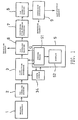
- A first embodiment of a sputtering apparatus according to the present invention will be described with reference to Figure 5 through Figure 7. In this embodiment, when the discharge power waveform has not been normal, i.e., when the sufficient discharge power necessary for the normal film deposition process has not been applied, the apparatus produces an abnormality-indicating signal corresponding to each substrate to be inspected which indicates that a defective substrate has been produced in the film deposition process. The entire manufacturing line, in which this embodiment of the sputtering apparatus has been employed, has the same configuration as that shown in Figure 1 and Figure 2. However, the
power source 34 has a configuration shown in Figure 5. In Figure 5, thepower source 34 receives 3-phase AC power, and converts the same into high-voltage DC power by use of an AC-DC converter 34a incorporated therein. The thus converted high-voltage DC power is supplied to thefilm deposition apparatus 3. The AC-DC converter 34a produces the DC power output in accordance with an output timing signal supplied from acontrol circuit board 34b. The output timing signal has been appropriately determined so as to perform the prescribed film deposition process. Further, a DC output power value Pa and a DC output voltage value Pr, which represent the converted output, are detected by use of a combination of components such as a resistor 34c, a voltage detection circuit 34ba and a current detection circuit 34bb. The thus detected values Pa and Pr are fed into the judging means 51 in thecontrol unit 5. Thus, the judging means 51 can judge whether or not the prescribed film deposition process has been satisfactorily performed. Moreover, thepower source 34 produces a spark signal Pk upon the detection of the fact that an arc discharge (abnormal discharge) has occurred during the sputtering process instead of a glow discharge (normal discharge). The spark signal Pk is also fed into the judging means 51 in thecontrol unit 5, as shown in Figure 5. - The judging means 51 feeds a discharge starting signal Hk and a discharge-stop controlling signal Ht into the
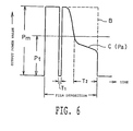
power source 34. Thepower source 34 then feeds an analog-detection output signal (Pa) corresponding to its output DC power into the judging means 51. In Figure 6, the rectangular waveform indicated by the dotted line B represents the prescribed DC output power to achieve the satisfactory film deposition. Assume that the analog-detection output signal (Pa) has a waveform indicated by the solid line C. This represents that the prescribed DC output power has not been supplied to thefilm deposition apparatus 3. Specifically, the total amount of times T1 and T2, in which the discharge power has not reached a minimum output power value Pt during a single sputtering process, has exceeded a predetermined constant time period L. In this case, the judging means 51 recognizes that the prescribed discharge power necessary for the normal film deposition process has not been supplied, and judges that the prescribed film deposition process has not been satisfactorily performed, and then feeds an abnormality-detection signal Q corresponding to the each substrate to be inspected into thesecond handling machine 6. Thus, a corresponding substrate having a defective thin film deposited thereon can be removed from thesecond handling machine 6. - The programmed control procedures with respect to the above-described operations in the judging means 51 will be described with reference to a flow chart shown in Figure 7. In STEP (a) and in STEP (b), the procedure respectively predetermines a prescribed DC output value Pm and a reference DC output value Pt. In STEP (c), the procedure receives the analog-detection output signal Pa from the
power source 34. In STEP (d), the procedure converts the thus received analog signal Pa into a digital signal. In STEP (e), the procedure calculates the total amount of time in which Pt ≧ Pa, i.e., the cause to prevent the normal film deposition process. In STEP (f), the procedure predetermines the discharge time period L necessary for the prescribed film deposition process. In STEP (g), the procedure calculates an actual total amount of time in which Pt ≧ Pa during a single film deposition process. In STEP (h), the procedure judges whether or not the thus calculated actual total amount of time has exceeded the predetermined time period L. In the case of YES, the procedure then produces an abnormality-detection signal Q, and feeds it to thesecond handling machine 6. Further, the procedure indicates this abnormality on thedisplay 52. Therefore, when the above-described second embodiment is employed in a series of manufacturing line processes, a substrate having a defective thin film deposited thereon can be removed from the line at the earliest possible step, i.e., at thesecond handling machine 6. This can be performed in the same manner as in the first embodiment. Thus, the load on thefinal inspection apparatus 9 can be reduced, and the wasteful processes in the line with respect to the defective substrates can be avoided. - Moreover, there can be provided another technique to judge whether or not the prescribed film deposition process has been satisfactorily performed on the basis of the detection results of whether or not the normal discharge has been performed during the film deposition process. Specifically, the technique is such that the total amount of time, in which the instantaneous discharge interruption (caused by are discharge and the like) has occurred during a single film deposition process, is compared with a predetermined allowable time. Further, when the total amount of time has exceeded the predetermined allowable time, the judging means 51 recognizes that the prescribed film deposition process has not been satisfactorily performed. The judging means 51 then produces an abnormality-detection signal. This technique is useful because even the instantaneous discharge interruption would have some adverse effect on the film deposition process which is performed in an extremely short period of about 2 seconds.
- Next, a second embodiment of a sputtering apparatus according to the present invention, in which the above-described technique is utilized, will be described with reference to Figure 8 and Figure 9. Figure 8 shows the waveform of the discharge power, and Figure 9 shows the programmed procedures in the judging means 51. In Figure 8, T3 and T4 respectively represent the times in which the instantaneous discharge interruption has occurred during a single film deposition process. The judging means 51 compares the total amount of such times, i.e., Tc = T3 + T4, with a predetermined reference time period L1, and judges whether or not Tc > L1. When Tc > L1, the judging means 51 then produces an abnormality-detection signal Q indicating that the entire normal discharge power has been insufficient for the satisfactory film deposition process. The programmed procedures shown in Figure 9 are substantially the same as those in the second embodiment shown in Figure 7, so that the detailed description thereof will be omitted. In Figure 9, the procedure predetermines the reference time period L1 (STEP(i)), and starts the discharge (STEP (j)). Thereafter, the procedure calculates the total amount of time, Tc =T3 + T4 (STEP (k)). In STEP (1), the procedure judges whether or not Tc > L1. When Tc > L1, the procedure recognizes that the prescribed film deposition process has not been satisfactorily performed, and produces the abnormality-detection signal Q, which is fed into the
second handling machine 6. Thus, a substrate having a defective thin film deposited thereon can be removed from thesecond handling machine 6. Further, the procedure indicates such abnormality on thedisplay 52. - Moreover, assume that the number of times of instantaneous discharge interruptions (caused by arc discharge and the like) in a single film deposition process has exceeded a predetermined allowable number. In this case, a prescribed thin film cannot be satisfactorily deposited on the surface of a substrate, and the pits formed thereon might be damaged. This phenomenon occurs because of the fact that the excessive number of times of instantaneous discharge interruptions causes aluminum to be scattered in massive particles from the parts such as an aluminum target, a protective shield and the like. Upon the detection of the excessive number of times of instantaneous discharge interruptions, the judging means 51 recognizes that unsatisfactory film deposition process has been performed, and produces an abnormality-detection signal.
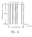
- Next, a third embodiment of a sputtering apparatus according to the present invention, in which the above-described phenomenon has been taken into consideration, will be described with reference to Figure 10 and Figure 11. Figure 10 shows the waveform of the discharge power, and Figure 11 shows the programmed procedures in the judging means 51. In Figure 10, instantaneous discharge interruptions (caused by sparks) have occurred five times (t1 through t5) during a single film deposition process. The judging means 51 counts the number of times of the instantaneous discharge interruptions, and compares the thus counted number n with a predetermined reference number of times L2. When n > L2, the judging means 51 then produces an abnormality-detection signal Q because the damage to the surface of the
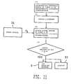
substrate 4 cannot be neglected even when the entire discharge power has been sufficient to achieve the prescribed film deposition process. In Figure 11, the procedure predetermines the reference number of times of instantaneous discharge interruptions (STEP (m)). After the discharge has been started, several spark signals Pk (indicating the occurrence of instantaneous discharge interruptions) are produced from thepower source 34. The procedure counts the number n of instantaneous discharge interruptions on the basis of the thus produced spark signals Pk (STEP (n)). The procedure judges whether or not the thus counted number n is greater than or equal to the reference number L2. When n ≧ L2, the procedure then produces an abnormality-detection signal Q, and feeds it both to thesecond handling machine 6 and the display 52 (STEP (o)). - In the above-described first through third embodiments, the
power source 34 has been described as the DC power source. However, thepower source 34 can also be replaced with a high frequency power source. In this case, the same advantages as those in the above-described embodiments can also be obtained. Further, in the second through fourth embodiments, the waveform of the output power Pa has been utilized to judge whether or not the prescribed film deposition process has been satisfactorily performed. However, the waveform of the output voltage Pr may also be utilized for the same judgment. Moreover, the abnormality-detection signal Q may also be fed into thethird handling machine 8. Further, in the respective above-described embodiments, various parameters, which are discharge power, discharge interruption time, the number of arc discharges and the discharge voltage value or the discharge current value, are independently and individually detected to be utilized as the basis of the abnormality-detection of the sputtering process. However, such parameters may also be appropriately selected so as to make a combination thereof, or all of the parameters may also be provided in the apparatus. Namely, in some cases, all of the above-described embodiments can be incorporated in the sputtering apparatus, the abnormality detection of the sputtering film deposition process can be performed either on the basis of a parameter of any one of the embodiments, or on the basis of a combination of plural parameters of the embodiments incorporated in the apparatus. - As described above, according to the present invention, there can be provided a sputtering apparatus that can judge, immediately after the completion on a film deposition process, whether or not the film deposition process has been satisfactorily performed, and can produce an abnormality-detection signal. Thus, when the sputtering apparatus of this invention is incorporated in a mass-production manufacturing line, a substrate having a defective film in terms of function and/or appearance, which cannot be detected by the conventional inspection apparatus, can be removed from the line at the earliest possible step. This is significantly advantageous, and contributes much to the improvement in the efficiency of the manufacturing line. The apparatus of this invention can also be utilized even for a single sputtering process, i.e., a sputtering apparatus for various objects such as a glass plate, a metal plate, plastics and the like. The sputtering apparatus according to the present invention having a simple configuration can assuredly detect the abnormalities in the film deposition process with respect to an individual substrate at the earliest possible step in the continuous manufacturing line. Thus, the apparatus is significantly advantageous to the practical applications.
- Obviously, numerous additional modifications and variations of the present invention are possible in light of the above teachings. It is therefore to be understood that within the scope of the appended claimes, the invention may be practiced otherwise than as specifically described herein.
Claims (7)
- A method of monitoring the deposition of a thin film onto a substrate (4) using a sputtering apparatus which comprises a deposition chamber (31) housing a target (33) of thin film depositing material, and a power source (34) for supplying discharge power across the substrate (4) and the target (33), characterized in that the method comprises :monitoring the discharge power waveform over a discharge time period during which power is applied for each thin film deposition;obtaining a value or values representing a change in the discharge power waveform during the time period; anddetermining whether the deposition of the thin film has been performed satisfactorily based on the value or values obtained.
- A method as claimed in claim 1, in which the change in the discharge power waveform during the time period comprises a drop in the power waveform below a predetermined level, the respective value comprising the total time of the discharge time period during which the power waveform is below the predetermined level.
- A method as claimed in claim 1 or 2, in which the change in the discharge power waveform during the time period comprises or further comprises an interruption in the power waveform, the respective value comprising the total time of the discharge time period during which the power waveform is interrupted.
- A method as claimed in claim 1, 2 or 3, in which the change in the discharge power waveform during the time period comprises or further comprises an arc discharge within the power waveform, the respective value comprising the total number of arc discharges during the discharge time period.
- A method as claimed in any one of claims 1 to 4, in which the discharge power waveform is monitored by monitoring a discharge voltage value.
- A method as claimed in any one of claims 1 to 4 , in which the discharge power waveform is monitored by monitoring a discharge current value.
- A method as claimed in any one of claims 1 to 6, further comprising the step of monitoring the pressure in the deposition chamber, and thereby obtaining a pressure value which is also used to determine whether the deposition of the thin film has been performed satisfactorily.
Applications Claiming Priority (2)
| Application Number | Priority Date | Filing Date | Title |
|---|---|---|---|
| JP3029431A JP2529031B2 (en) | 1991-01-30 | 1991-01-30 | Sputtering equipment |
| JP29431/91 | 1991-01-30 |
Publications (2)
| Publication Number | Publication Date |
|---|---|
| EP0497066A1 EP0497066A1 (en) | 1992-08-05 |
| EP0497066B1 true EP0497066B1 (en) | 1996-06-12 |
Family
ID=12275954
Family Applications (1)
| Application Number | Title | Priority Date | Filing Date |
|---|---|---|---|
| EP91402591A Expired - Lifetime EP0497066B1 (en) | 1991-01-30 | 1991-09-27 | A sputtering apparatus |
Country Status (4)
| Country | Link |
|---|---|
| US (1) | US5336385A (en) |
| EP (1) | EP0497066B1 (en) |
| JP (1) | JP2529031B2 (en) |
| DE (1) | DE69120242T2 (en) |
Families Citing this family (17)
| Publication number | Priority date | Publication date | Assignee | Title |
|---|---|---|---|---|
| US5766360A (en) * | 1992-03-27 | 1998-06-16 | Kabushiki Kaisha Toshiba | Substrate processing apparatus and substrate processing method |
| US5757494A (en) * | 1994-10-21 | 1998-05-26 | J.A. Woollam Co. Inc. | System and method for improving data acquisition capability in spectroscopic ellipsometers |
| US5956145A (en) * | 1992-09-18 | 1999-09-21 | J. A. Woollam Co. Inc. | System and method for improving data acquisition capability in spectroscopic rotatable element, rotating element, modulation element, and other ellipsometer and polarimeter and the like systems |
| US6516742B1 (en) * | 1998-02-26 | 2003-02-11 | Micron Technology, Inc. | Apparatus for improved low pressure inductively coupled high density plasma reactor |
| US6440280B1 (en) | 2000-06-28 | 2002-08-27 | Sola International, Inc. | Multi-anode device and methods for sputter deposition |
| US6816749B2 (en) * | 2000-12-22 | 2004-11-09 | Fuji Photo Film Co., Ltd. | Method of and apparatus for manufacturing rolled medium products |
| US6395093B1 (en) | 2001-07-19 | 2002-05-28 | The Regents Of The University Of California | Self contained, independent, in-vacuum spinner motor |
| WO2004001094A1 (en) * | 2002-06-19 | 2003-12-31 | Tosoh Smd, Inc. | Sputter target monitoring system |
| JP4582711B2 (en) * | 2005-08-30 | 2010-11-17 | 芝浦メカトロニクス株式会社 | Vacuum processing apparatus and vacuum processing method |
| TWI400347B (en) * | 2007-08-10 | 2013-07-01 | Hon Hai Prec Ind Co Ltd | Apparatus and method of sputtering deposition |
| TWI399448B (en) * | 2007-09-21 | 2013-06-21 | Hon Hai Prec Ind Co Ltd | Aparatus and method of sputtering deposition |
| US20110120917A1 (en) * | 2009-11-24 | 2011-05-26 | Chevron U.S.A. Inc. | Hydrogenation of solid carbonaceous materials using mixed catalysts |
| JP5611027B2 (en) * | 2010-12-24 | 2014-10-22 | 小島プレス工業株式会社 | Resin product manufacturing system |
| ITMI20110432A1 (en) * | 2011-03-18 | 2012-09-19 | Tapematic Spa | MACHINE AND METHOD FOR THE METALLIZATION OF THREE-DIMENSIONAL OBJECTS OF SMALL DIMENSIONS |
| JP6459858B2 (en) * | 2015-08-28 | 2019-01-30 | 住友金属鉱山株式会社 | Long substrate processing apparatus, control method therefor, and method for manufacturing long substrate with metal film using the control method |
| CN110534428B (en) * | 2019-09-05 | 2022-02-15 | 武汉新芯集成电路制造有限公司 | Method for manufacturing metal layer structure, semiconductor device and method for manufacturing semiconductor device |
| KR102864016B1 (en) * | 2020-11-25 | 2025-09-23 | 어플라이드 머티어리얼스, 인코포레이티드 | Waveform shape factor for pulsed PVD power |
Family Cites Families (14)
| Publication number | Priority date | Publication date | Assignee | Title |
|---|---|---|---|---|
| JPS5729577A (en) * | 1980-07-30 | 1982-02-17 | Anelva Corp | Automatic continuous sputtering apparatus |
| JPS5941475A (en) * | 1982-09-02 | 1984-03-07 | Ulvac Corp | Apparatus for monitoring discharge state in discharge treatment apparatus |
| US4500408A (en) * | 1983-07-19 | 1985-02-19 | Varian Associates, Inc. | Apparatus for and method of controlling sputter coating |
| BG41744A1 (en) * | 1984-11-26 | 1987-08-14 | Savov | Method for control of chimico= thermic processing of work- pieces with glowing dicharge in medium of processing gas and device for implementing this method |
| US4663009A (en) * | 1985-02-08 | 1987-05-05 | Hewlett-Packard Company | System and method for depositing plural thin film layers on a substrate |
| US4749465A (en) * | 1985-05-09 | 1988-06-07 | Seagate Technology | In-line disk sputtering system |
| US4894133A (en) * | 1985-11-12 | 1990-01-16 | Virgle L. Hedgcoth | Method and apparatus making magnetic recording disk |
| US4858556A (en) * | 1986-09-15 | 1989-08-22 | Siebert Jerome F | Method and apparatus for physical vapor deposition of thin films |
| US4847792A (en) * | 1987-05-04 | 1989-07-11 | Texas Instruments Incorporated | Process and apparatus for detecting aberrations in production process operations |
| US4849087A (en) * | 1988-02-11 | 1989-07-18 | Southwall Technologies | Apparatus for obtaining transverse uniformity during thin film deposition on extended substrate |
| JPH02205675A (en) * | 1989-02-02 | 1990-08-15 | Toshiba Corp | Reactive sputtering device |
| US4957605A (en) * | 1989-04-17 | 1990-09-18 | Materials Research Corporation | Method and apparatus for sputter coating stepped wafers |
| JPH04141584A (en) * | 1990-10-02 | 1992-05-15 | Clarion Co Ltd | Sputtering device |
| JPH04165068A (en) * | 1990-10-26 | 1992-06-10 | Nec Kyushu Ltd | Sputtering system |
-
1991
- 1991-01-30 JP JP3029431A patent/JP2529031B2/en not_active Expired - Lifetime
- 1991-09-27 EP EP91402591A patent/EP0497066B1/en not_active Expired - Lifetime
- 1991-09-27 DE DE69120242T patent/DE69120242T2/en not_active Expired - Fee Related
-
1993
- 1993-01-08 US US08/003,860 patent/US5336385A/en not_active Expired - Lifetime
Also Published As
| Publication number | Publication date |
|---|---|
| US5336385A (en) | 1994-08-09 |
| JP2529031B2 (en) | 1996-08-28 |
| JPH05230652A (en) | 1993-09-07 |
| EP0497066A1 (en) | 1992-08-05 |
| DE69120242T2 (en) | 1996-11-28 |
| DE69120242D1 (en) | 1996-07-18 |
Similar Documents
| Publication | Publication Date | Title |
|---|---|---|
| US5336385A (en) | Sputtering apparatus | |
| US5993615A (en) | Method and apparatus for detecting arcs | |
| US6313583B1 (en) | Plasma processing apparatus and method | |
| US7988833B2 (en) | System and method for detecting non-cathode arcing in a plasma generation apparatus | |
| US10607821B2 (en) | Sputtering system and method including an arc detection | |
| US5584974A (en) | Arc control and switching element protection for pulsed dc cathode sputtering power supply | |
| EP1441576B1 (en) | Method for detecting an arc in a glow discharg apparatus and high-frequency arc discharge suppressor | |
| US20050236266A1 (en) | Sputter target monitoring system | |
| JP3893276B2 (en) | Plasma processing equipment | |
| WO2008034092A2 (en) | System and method for detecting non-cathode arcing in a plasma generation apparatus | |
| CN117501403A (en) | Signal processing system and power supply device with signal processing system | |
| US6080292A (en) | Monitoring apparatus for plasma process | |
| JPH08330095A (en) | Plasma processing device | |
| US6032544A (en) | Automated particle monitor for a thin film process | |
| WO1999022397A1 (en) | Arc monitoring | |
| US20100166980A1 (en) | Inline vacuum processing apparatus, method of controlling the same, and information recording medium manufacturing method | |
| JPH1088338A (en) | Arc counting device | |
| CN119601446B (en) | Method and device for detecting electric arc of plasma processing chamber | |
| JP2738769B2 (en) | End point judgment method | |
| JPH11144337A (en) | Optical recording medium manufacturing apparatus, optical recording medium manufacturing method, and optical recording medium | |
| JP2002226965A (en) | Sputtering method | |
| US7282122B2 (en) | Method and system for target lifetime | |
| JP2002294444A (en) | Film forming apparatus and program for film forming apparatus | |
| EP0300089B1 (en) | Automatic ejector rate normalizer | |
| JPH0512725A (en) | Optical disk molding method and molding apparatus |
Legal Events
| Date | Code | Title | Description |
|---|---|---|---|
| PUAI | Public reference made under article 153(3) epc to a published international application that has entered the european phase |
Free format text: ORIGINAL CODE: 0009012 |
|
| 17P | Request for examination filed |
Effective date: 19911002 |
|
| AK | Designated contracting states |
Kind code of ref document: A1 Designated state(s): DE FR GB |
|
| RAP1 | Party data changed (applicant data changed or rights of an application transferred) |
Owner name: SHIBAURA ENGINEERING WORKS CO., LTD. Owner name: SONY CORPORATION |
|
| 17Q | First examination report despatched |
Effective date: 19940906 |
|
| GRAH | Despatch of communication of intention to grant a patent |
Free format text: ORIGINAL CODE: EPIDOS IGRA |
|
| GRAH | Despatch of communication of intention to grant a patent |
Free format text: ORIGINAL CODE: EPIDOS IGRA |
|
| GRAA | (expected) grant |
Free format text: ORIGINAL CODE: 0009210 |
|
| AK | Designated contracting states |
Kind code of ref document: B1 Designated state(s): DE FR GB |
|
| REF | Corresponds to: |
Ref document number: 69120242 Country of ref document: DE Date of ref document: 19960718 |
|
| ET | Fr: translation filed | ||
| PLBE | No opposition filed within time limit |
Free format text: ORIGINAL CODE: 0009261 |
|
| STAA | Information on the status of an ep patent application or granted ep patent |
Free format text: STATUS: NO OPPOSITION FILED WITHIN TIME LIMIT |
|
| 26N | No opposition filed | ||
| PGFP | Annual fee paid to national office [announced via postgrant information from national office to epo] |
Ref country code: FR Payment date: 20010928 Year of fee payment: 11 |
|
| REG | Reference to a national code |
Ref country code: GB Ref legal event code: IF02 |
|
| PG25 | Lapsed in a contracting state [announced via postgrant information from national office to epo] |
Ref country code: FR Free format text: LAPSE BECAUSE OF NON-PAYMENT OF DUE FEES Effective date: 20030603 |
|
| REG | Reference to a national code |
Ref country code: FR Ref legal event code: ST |
|
| PGFP | Annual fee paid to national office [announced via postgrant information from national office to epo] |
Ref country code: GB Payment date: 20080822 Year of fee payment: 18 |
|
| PGFP | Annual fee paid to national office [announced via postgrant information from national office to epo] |
Ref country code: DE Payment date: 20080911 Year of fee payment: 18 |
|
| GBPC | Gb: european patent ceased through non-payment of renewal fee |
Effective date: 20090927 |
|
| PG25 | Lapsed in a contracting state [announced via postgrant information from national office to epo] |
Ref country code: DE Free format text: LAPSE BECAUSE OF NON-PAYMENT OF DUE FEES Effective date: 20100401 |
|
| PG25 | Lapsed in a contracting state [announced via postgrant information from national office to epo] |
Ref country code: GB Free format text: LAPSE BECAUSE OF NON-PAYMENT OF DUE FEES Effective date: 20090927 |