EP0493015A2 - LED array type light source - Google Patents
LED array type light source Download PDFInfo
- Publication number
- EP0493015A2 EP0493015A2 EP91311863A EP91311863A EP0493015A2 EP 0493015 A2 EP0493015 A2 EP 0493015A2 EP 91311863 A EP91311863 A EP 91311863A EP 91311863 A EP91311863 A EP 91311863A EP 0493015 A2 EP0493015 A2 EP 0493015A2
- Authority
- EP
- European Patent Office
- Prior art keywords
- led
- light
- amount
- light source
- regulating
- Prior art date
- Legal status (The legal status is an assumption and is not a legal conclusion. Google has not performed a legal analysis and makes no representation as to the accuracy of the status listed.)
- Granted
Links
Images


Classifications
-
- H—ELECTRICITY
- H04—ELECTRIC COMMUNICATION TECHNIQUE
- H04N—PICTORIAL COMMUNICATION, e.g. TELEVISION
- H04N1/00—Scanning, transmission or reproduction of documents or the like, e.g. facsimile transmission; Details thereof
- H04N1/024—Details of scanning heads ; Means for illuminating the original
- H04N1/028—Details of scanning heads ; Means for illuminating the original for picture information pick-up
- H04N1/02815—Means for illuminating the original, not specific to a particular type of pick-up head
- H04N1/02845—Means for illuminating the original, not specific to a particular type of pick-up head using an elongated light source, e.g. tubular lamp, LED array
- H04N1/02865—Means for illuminating the original, not specific to a particular type of pick-up head using an elongated light source, e.g. tubular lamp, LED array using an array of light sources or a combination of such arrays, e.g. an LED bar
-
- H—ELECTRICITY
- H04—ELECTRIC COMMUNICATION TECHNIQUE
- H04N—PICTORIAL COMMUNICATION, e.g. TELEVISION
- H04N1/00—Scanning, transmission or reproduction of documents or the like, e.g. facsimile transmission; Details thereof
- H04N1/024—Details of scanning heads ; Means for illuminating the original
- H04N1/028—Details of scanning heads ; Means for illuminating the original for picture information pick-up
- H04N1/02815—Means for illuminating the original, not specific to a particular type of pick-up head
-
- H—ELECTRICITY
- H10—SEMICONDUCTOR DEVICES; ELECTRIC SOLID-STATE DEVICES NOT OTHERWISE PROVIDED FOR
- H10H—INORGANIC LIGHT-EMITTING SEMICONDUCTOR DEVICES HAVING POTENTIAL BARRIERS
- H10H29/00—Integrated devices, or assemblies of multiple devices, comprising at least one light-emitting semiconductor element covered by group H10H20/00
- H10H29/10—Integrated devices comprising at least one light-emitting semiconductor component covered by group H10H20/00
- H10H29/14—Integrated devices comprising at least one light-emitting semiconductor component covered by group H10H20/00 comprising multiple light-emitting semiconductor components
- H10H29/142—Two-dimensional arrangements, e.g. asymmetric LED layout
-
- H—ELECTRICITY
- H10—SEMICONDUCTOR DEVICES; ELECTRIC SOLID-STATE DEVICES NOT OTHERWISE PROVIDED FOR
- H10W—GENERIC PACKAGES, INTERCONNECTIONS, CONNECTORS OR OTHER CONSTRUCTIONAL DETAILS OF DEVICES COVERED BY CLASS H10
- H10W90/00—Package configurations
-
- H—ELECTRICITY
- H10—SEMICONDUCTOR DEVICES; ELECTRIC SOLID-STATE DEVICES NOT OTHERWISE PROVIDED FOR
- H10H—INORGANIC LIGHT-EMITTING SEMICONDUCTOR DEVICES HAVING POTENTIAL BARRIERS
- H10H20/00—Individual inorganic light-emitting semiconductor devices having potential barriers, e.g. light-emitting diodes [LED]
- H10H20/80—Constructional details
- H10H20/81—Bodies
- H10H20/813—Bodies having a plurality of light-emitting regions, e.g. multi-junction LEDs or light-emitting devices having photoluminescent regions within the bodies
Definitions
- the present invention relates to an LED array type light source particularly suitable for use in image sensors and the like.
- a light source comprising a plurality of LED's (light emitting diodes).
- the plurality of LED's are arranged into a linear light source which comprises a plurality of LED chip trains juxtaposed, each of the LED chip trains including a plurality of LED chips connected in series with one another.
- the optical output of each of the LED chips may be different from those of the other LED chips due to irregular epitaxial growth or the like. It is therefore important how the optical outputs of the LED chip trains are equalized.
- the selection of the current regulating resistor 2 is made through the following process.
- a wiring pattern is first formed on a dielectric substrate.
- LED chips 1 are then die bonded on the substrate.
- the LED chips 1 are wire bonded to the wiring pattern and also connected in series with one another.
- a probe is applied to the LED chips 1 so that they are energized to emit light.
- a resistance for optimizing the amount of light in the LED chips 1 is determined.
- a chip resistor R having a resistance nearest to the optimum resistance is then selected and mounted on the substrate so that the plurality of LED chips 1 are connected in series with the current regulating resistor 2. Since the resistances of the current regulating resistor 2 are limited, however, it is difficult to accurately regulate the amount of light emitted by the LED chips 1.
- the current regulating resistor 2 is replaced by a train of silicon chip resistors 3 connected in series with the plurality of LED chips 1, as shown in Fig. 5.
- One or more silicon chip resistors 3 are selected from the train so that a resistance nearest to the optimum resistance will be provided. Only the selected silicon chip resistors are bonded to the substrate. See Japanese Utility Model Application No. Hei 1-87590 which has been filed by the applicant.
- the present invention provides an LED array type light source comprising a substrate, a group of LED chips comprising a plurality of juxtaposed LED chip trains, each of said LED chip trains including a plurality of serially connected LED chips, a plurality of first regulating resistors, each of said first regulating resistors being connected in series with one of said LED chip trains to independently regulate the amount of light in that LED chip train, and a second regulating resistor serially connected in common to said first regulating resistors so that the total amount of light in said group of LED chips can be regulated.
- the LED array type light source of the present invention includes the first and second regulating resistor means, a desired amount of light through the entire light source system can be simply and readily attained by first equalizing the amount of light in each LED chip train to those of the other LED chip trains and regulating the total amount of light through the light source with the second regulating resistor.
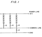
- Fig. 1 is a circuit diagram of one embodiment of an LED array type light source constructed in accordance with the present invention.
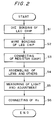
- Fig. 2 is a flow chart illustrating a process of producing the LED array type light source shown in Fig. 1.
- Fig. 3 is a flow chart illustrating a process of calculating a common resistor in the LED array type light source shown in Fig. 1.
- Fig. 4 is a circuit diagram of an LED array type light source constructed in accordance with the prior art.
- Fig. 5 is a circuit diagram of another LED array type light source constructed in accordance with the prior art.
- An LED array type light source shown in Fig. 1 may be produced by following a procedure shown in the flow chart of Fig. 2.
- a plurality of LED chips formed from the same wafer are first die bonded onto a substrate (S1).
- Each of the LED chips is then wire bonded to a wiring pattern formed on the substrate and connected in series with the other LED chips (S2).
- Fig. 1 shows three LED chip trains each comprising four LED chips connected in series with one another.
- a first regulating resistor 10 having a given fixed resistance is connected in series with each of the three LED chip trains to form an LED array.
- Each of the LED arrays is connected, at one end, with a power line, the other end of that LED array being connected with a common line (S3).
- the first regulating resistors 10 are connected in series or directly with the respective LED chip trains so that each of the LED chip trains will receive substantially the same current, there will be very little difference in the amount of light emitted for the same current when the LED chips are formed from the same wafer. As a result, there is substantially no difference in the amount of light between the LED chip trains.
- a common resistor 12 is connected in series with the first regulating resistors 10 between the common line and GND to make the amount of light through the entire light source system a desired level.
- the resistance of such a common resistor 12 will be calculated through the following procedure (S5 and S6 in Fig. 2).
- a current to be applied to the respective LED chip trains is first set (S101).
- Light emitted through the plastic lens is then measured (S102).
- S103 it is judged whether or not the measured light is at a desired level. If not, the current level set at the step S101 is changed to another level (S104). The measurement of light is again carried out.
- a voltage between the power line and the common line is then calculated (S105). If it is assumed at this time that a voltage between the power line and the common line is V1 and the supply voltage is V (which is usually equal to 12 volts in image sensor light sources such as facsimile machines and the like), a resistance R to be used in the common resistor 12 can be calculated (at S106) from an equation:
- R (V - V1)/I where I is an applied current set at the step S101 or S104.
- the common resistor 12 having such a resistance R will be connected between the common line and the GND (S6).
Landscapes
- Engineering & Computer Science (AREA)
- Multimedia (AREA)
- Signal Processing (AREA)
- Led Devices (AREA)
- Facsimile Scanning Arrangements (AREA)
- Image Input (AREA)
- Led Device Packages (AREA)
Abstract
Description
- The present invention relates to an LED array type light source particularly suitable for use in image sensors and the like.
- In conventional image sensors for reading original documents, such as facsimile machines and the like, it is normal to utilize a light source comprising a plurality of LED's (light emitting diodes). Usually, the plurality of LED's are arranged into a linear light source which comprises a plurality of LED chip trains juxtaposed, each of the LED chip trains including a plurality of LED chips connected in series with one another. However, the optical output of each of the LED chips may be different from those of the other LED chips due to irregular epitaxial growth or the like. It is therefore important how the optical outputs of the LED chip trains are equalized.
- A proposal has been made that a plurality of LED chips 1 connected in series with one another are connected in series with a current regulating
resistor 2 as shown in Fig. 4. Such a proposal is intended to provide an equal amount of light from each LED strip by driving them with a constant voltage. - Usually, the selection of the current regulating
resistor 2 is made through the following process. A wiring pattern is first formed on a dielectric substrate. LED chips 1 are then die bonded on the substrate. The LED chips 1 are wire bonded to the wiring pattern and also connected in series with one another. Thereafter, a probe is applied to the LED chips 1 so that they are energized to emit light. A resistance for optimizing the amount of light in the LED chips 1 is determined. A chip resistor R having a resistance nearest to the optimum resistance is then selected and mounted on the substrate so that the plurality of LED chips 1 are connected in series with the current regulatingresistor 2. Since the resistances of the current regulatingresistor 2 are limited, however, it is difficult to accurately regulate the amount of light emitted by the LED chips 1. - In order to overcome such a problem, another proposal has been made that the current regulating
resistor 2 is replaced by a train of silicon chip resistors 3 connected in series with the plurality of LED chips 1, as shown in Fig. 5. One or more silicon chip resistors 3 are selected from the train so that a resistance nearest to the optimum resistance will be provided. Only the selected silicon chip resistors are bonded to the substrate. See Japanese Utility Model Application No. Hei 1-87590 which has been filed by the applicant. - When the train of silicon chip resistors 3 are connected to the substrate in such a manner, the amount of light in the LED chips 1 can be regulated extremely accurately. However, such an arrangement increases the time required to regulate the amount of light since it requires various processes, namely light measuring, resistor selecting and bonding.
- It is therefore an object of an embodiment of the present invnetion to provide an LED array type light source which can finely regulate the amount of light emitted through a simplified process.
- The present invention provides an LED array type light source comprising a substrate, a group of LED chips comprising a plurality of juxtaposed LED chip trains, each of said LED chip trains including a plurality of serially connected LED chips, a plurality of first regulating resistors, each of said first regulating resistors being connected in series with one of said LED chip trains to independently regulate the amount of light in that LED chip train, and a second regulating resistor serially connected in common to said first regulating resistors so that the total amount of light in said group of LED chips can be regulated.
- Since the LED array type light source of the present invention includes the first and second regulating resistor means, a desired amount of light through the entire light source system can be simply and readily attained by first equalizing the amount of light in each LED chip train to those of the other LED chip trains and regulating the total amount of light through the light source with the second regulating resistor.
- An example of the present invention will now be described with reference to the accompanying drawings in which:
- Fig. 1 is a circuit diagram of one embodiment of an LED array type light source constructed in accordance with the present invention.
- Fig. 2 is a flow chart illustrating a process of producing the LED array type light source shown in Fig. 1.
- Fig. 3 is a flow chart illustrating a process of calculating a common resistor in the LED array type light source shown in Fig. 1.
- Fig. 4 is a circuit diagram of an LED array type light source constructed in accordance with the prior art.
- Fig. 5 is a circuit diagram of another LED array type light source constructed in accordance with the prior art.
- An LED array type light source shown in Fig. 1 may be produced by following a procedure shown in the flow chart of Fig. 2. A plurality of LED chips formed from the same wafer are first die bonded onto a substrate (S1). Each of the LED chips is then wire bonded to a wiring pattern formed on the substrate and connected in series with the other LED chips (S2). Fig. 1 shows three LED chip trains each comprising four LED chips connected in series with one another.
- A first regulating
resistor 10 having a given fixed resistance is connected in series with each of the three LED chip trains to form an LED array. Each of the LED arrays is connected, at one end, with a power line, the other end of that LED array being connected with a common line (S3). - After the LED arrays are covered and protected by any suitable plastic material, necessary parts such as plastic lens and others are mounted on the circuit substrate (S4).
- Since the first regulating
resistors 10 are connected in series or directly with the respective LED chip trains so that each of the LED chip trains will receive substantially the same current, there will be very little difference in the amount of light emitted for the same current when the LED chips are formed from the same wafer. As a result, there is substantially no difference in the amount of light between the LED chip trains. - After the first regulating
resistors 10 are respectively connected in series with the LED chip trains to equalize the amount of light through the LED chip trains, acommon resistor 12 is connected in series with the first regulatingresistors 10 between the common line and GND to make the amount of light through the entire light source system a desired level. The resistance of such acommon resistor 12 will be calculated through the following procedure (S5 and S6 in Fig. 2). - As shown in Fig. 3, a current to be applied to the respective LED chip trains is first set (S101). Light emitted through the plastic lens is then measured (S102). At the next step (S103), it is judged whether or not the measured light is at a desired level. If not, the current level set at the step S101 is changed to another level (S104). The measurement of light is again carried out.
- If the desired level of light is attained by repeating the above steps, a voltage between the power line and the common line is then calculated (S105). If it is assumed at this time that a voltage between the power line and the common line is V1 and the supply voltage is V (which is usually equal to 12 volts in image sensor light sources such as facsimile machines and the like), a resistance R to be used in the
common resistor 12 can be calculated (at S106) from an equation: - R = (V - V1)/I
where I is an applied current set at the step S101 or S104. - The
common resistor 12 having such a resistance R will be connected between the common line and the GND (S6). - When only one type of first regulating resistors for equalizing any difference in the amount of light through the group of LED chips are connected with the respective LED chip trains or no resistor is connected with the LED chip trains and if a common resistor for regulating the amount of light through the entire light source is connected between the common line and the GND, a desired amount of light can be easily provided. This in turn provides an LED array type light source of high quality which can be produced more simply and inexpensively.
Claims (1)
- An LED array type light source comprising:(a) a substrate;(b) a group of LED chips comprising a plurality of juxtaposed LED chip trains, each of said LED chip trains including a plurality of serially connected LED chips;(c) a plurality of first regulating resistors, each of said first regulating resistors being connected in series to the respective one of said LED chip trains to regulate the amount of light in that LED chip train independently; and(d) a second regulating resistor serially connected in common to said first regulating resistors so that the total amount of light in said group of LED chips can be regulated.
Applications Claiming Priority (2)
| Application Number | Priority Date | Filing Date | Title |
|---|---|---|---|
| JP406620/90 | 1990-12-26 | ||
| JP2406620A JP2549205B2 (en) | 1990-12-26 | 1990-12-26 | LED array light source |
Publications (3)
| Publication Number | Publication Date |
|---|---|
| EP0493015A2 true EP0493015A2 (en) | 1992-07-01 |
| EP0493015A3 EP0493015A3 (en) | 1992-12-23 |
| EP0493015B1 EP0493015B1 (en) | 1996-03-13 |
Family
ID=18516240
Family Applications (1)
| Application Number | Title | Priority Date | Filing Date |
|---|---|---|---|
| EP91311863A Revoked EP0493015B1 (en) | 1990-12-26 | 1991-12-20 | LED array type light source |
Country Status (4)
| Country | Link |
|---|---|
| EP (1) | EP0493015B1 (en) |
| JP (1) | JP2549205B2 (en) |
| KR (1) | KR100238515B1 (en) |
| DE (1) | DE69117909T2 (en) |
Cited By (3)
| Publication number | Priority date | Publication date | Assignee | Title |
|---|---|---|---|---|
| US6153980A (en) * | 1999-11-04 | 2000-11-28 | Philips Electronics North America Corporation | LED array having an active shunt arrangement |
| WO2008040300A1 (en) * | 2006-09-28 | 2008-04-10 | Osram Opto Semiconductors Gmbh | Led semiconductor body and use of an led semiconductor body |
| CN101118920B (en) * | 2006-08-02 | 2010-07-21 | 海立尔股份有限公司 | Sub-adhesive substrate and high-voltage light-emitting diode chip with impedance element |
Families Citing this family (2)
| Publication number | Priority date | Publication date | Assignee | Title |
|---|---|---|---|---|
| KR102036347B1 (en) | 2013-02-12 | 2019-10-24 | 삼성전자 주식회사 | LED array unit and LED module comprising the same |
| US9273995B2 (en) | 2014-02-04 | 2016-03-01 | Excelitas Technologies Philippines, Inc. | Light emitting diode output power control |
Family Cites Families (2)
| Publication number | Priority date | Publication date | Assignee | Title |
|---|---|---|---|---|
| JPH01146248U (en) * | 1988-03-29 | 1989-10-09 | ||
| JPH02220559A (en) * | 1989-02-21 | 1990-09-03 | Seiko Epson Corp | line sensor |
-
1990
- 1990-12-26 JP JP2406620A patent/JP2549205B2/en not_active Expired - Fee Related
-
1991
- 1991-12-04 KR KR1019910022186A patent/KR100238515B1/en not_active Expired - Fee Related
- 1991-12-20 DE DE69117909T patent/DE69117909T2/en not_active Revoked
- 1991-12-20 EP EP91311863A patent/EP0493015B1/en not_active Revoked
Cited By (6)
| Publication number | Priority date | Publication date | Assignee | Title |
|---|---|---|---|---|
| US6153980A (en) * | 1999-11-04 | 2000-11-28 | Philips Electronics North America Corporation | LED array having an active shunt arrangement |
| CN101118920B (en) * | 2006-08-02 | 2010-07-21 | 海立尔股份有限公司 | Sub-adhesive substrate and high-voltage light-emitting diode chip with impedance element |
| WO2008040300A1 (en) * | 2006-09-28 | 2008-04-10 | Osram Opto Semiconductors Gmbh | Led semiconductor body and use of an led semiconductor body |
| US8283684B2 (en) | 2006-09-28 | 2012-10-09 | Osram Opto Semiconductors Gmbh | LED semiconductor body and use of an LED semiconductor body |
| TWI384644B (en) * | 2006-09-28 | 2013-02-01 | 歐斯朗奧托半導體股份有限公司 | LED semiconductor body and application of LED semiconductor body |
| CN101563778B (en) * | 2006-09-28 | 2014-07-09 | 奥斯兰姆奥普托半导体有限责任公司 | LED semiconductor body and use of an LED semiconductor body |
Also Published As
| Publication number | Publication date |
|---|---|
| JPH04223762A (en) | 1992-08-13 |
| EP0493015B1 (en) | 1996-03-13 |
| DE69117909D1 (en) | 1996-04-18 |
| EP0493015A3 (en) | 1992-12-23 |
| DE69117909T2 (en) | 1996-08-22 |
| JP2549205B2 (en) | 1996-10-30 |
| KR100238515B1 (en) | 2000-01-15 |
| KR920014367A (en) | 1992-07-30 |
Similar Documents
| Publication | Publication Date | Title |
|---|---|---|
| US5150016A (en) | LED light source with easily adjustable luminous energy | |
| EP0307994B1 (en) | An exposure device with an aging correction system for a led printer | |
| EP0342814B1 (en) | Mos integrated circuit for driving light-emitting diodes | |
| EP0310266A2 (en) | Recalibration system for led array | |
| US5229870A (en) | Light emitting device capable of readily controlling total quantity of light under a balanced light emitting state of light emitting elements | |
| EP0493015B1 (en) | LED array type light source | |
| US5724055A (en) | Display apparatus and method of manufacture in which display luminance can be adjusted | |
| EP0487715B1 (en) | L.e.d. array printer | |
| JPS6234468Y2 (en) | ||
| US5699103A (en) | Method for producing a calibrated array of light-emitting diodes and apparatus including the calibrated array | |
| US6717604B2 (en) | Array driving circuit with control voltage adjusted at both ends, and array head using same | |
| US6169279B1 (en) | Image sensor chip, method for manufacturing the same, and image sensor therefor | |
| JPH04132275A (en) | Light emitting diode light source | |
| US20030142195A1 (en) | Optical fixing unit, illuminance correcting method for the same, and thermal printer | |
| KR20010101584A (en) | Linear light source and image reading device provided with this | |
| JP2934694B2 (en) | Image reading device | |
| JP5031155B2 (en) | Optical printer head and image forming apparatus using the same | |
| JP2813037B2 (en) | Image forming apparatus manufacturing method and manufacturing apparatus | |
| JPS622770A (en) | optical reader | |
| JPH0649378B2 (en) | Record head | |
| JP3588208B2 (en) | Optical printer head | |
| JPH0397276A (en) | Light-emitting diode array device | |
| WO2002097382A2 (en) | In situ calibration of photodiodes | |
| JPS63138788A (en) | Led array | |
| JPS61179664A (en) | Method for controlling luminous quantity of light emitting element array |
Legal Events
| Date | Code | Title | Description |
|---|---|---|---|
| PUAI | Public reference made under article 153(3) epc to a published international application that has entered the european phase |
Free format text: ORIGINAL CODE: 0009012 |
|
| AK | Designated contracting states |
Kind code of ref document: A2 Designated state(s): DE FR GB |
|
| PUAL | Search report despatched |
Free format text: ORIGINAL CODE: 0009013 |
|
| AK | Designated contracting states |
Kind code of ref document: A3 Designated state(s): DE FR GB |
|
| 17P | Request for examination filed |
Effective date: 19930112 |
|
| 17Q | First examination report despatched |
Effective date: 19950504 |
|
| GRAA | (expected) grant |
Free format text: ORIGINAL CODE: 0009210 |
|
| AK | Designated contracting states |
Kind code of ref document: B1 Designated state(s): DE FR GB |
|
| REF | Corresponds to: |
Ref document number: 69117909 Country of ref document: DE Date of ref document: 19960418 |
|
| ET | Fr: translation filed | ||
| PLBI | Opposition filed |
Free format text: ORIGINAL CODE: 0009260 |
|
| PLBF | Reply of patent proprietor to notice(s) of opposition |
Free format text: ORIGINAL CODE: EPIDOS OBSO |
|
| 26 | Opposition filed |
Opponent name: SIEMENS AG Effective date: 19961213 |
|
| PLBF | Reply of patent proprietor to notice(s) of opposition |
Free format text: ORIGINAL CODE: EPIDOS OBSO |
|
| PGFP | Annual fee paid to national office [announced via postgrant information from national office to epo] |
Ref country code: FR Payment date: 19981209 Year of fee payment: 8 |
|
| PGFP | Annual fee paid to national office [announced via postgrant information from national office to epo] |
Ref country code: GB Payment date: 19981224 Year of fee payment: 8 |
|
| PGFP | Annual fee paid to national office [announced via postgrant information from national office to epo] |
Ref country code: DE Payment date: 19981229 Year of fee payment: 8 |
|
| RDAH | Patent revoked |
Free format text: ORIGINAL CODE: EPIDOS REVO |
|
| RDAG | Patent revoked |
Free format text: ORIGINAL CODE: 0009271 |
|
| STAA | Information on the status of an ep patent application or granted ep patent |
Free format text: STATUS: PATENT REVOKED |
|
| 27W | Patent revoked |
Effective date: 19981202 |
|
| GBPR | Gb: patent revoked under art. 102 of the ep convention designating the uk as contracting state |
Free format text: 981202 |
|
| PLAB | Opposition data, opponent's data or that of the opponent's representative modified |
Free format text: ORIGINAL CODE: 0009299OPPO |