EP0492462A2 - Waveform detecting circuit - Google Patents
Waveform detecting circuit Download PDFInfo
- Publication number
- EP0492462A2 EP0492462A2 EP91121840A EP91121840A EP0492462A2 EP 0492462 A2 EP0492462 A2 EP 0492462A2 EP 91121840 A EP91121840 A EP 91121840A EP 91121840 A EP91121840 A EP 91121840A EP 0492462 A2 EP0492462 A2 EP 0492462A2
- Authority
- EP
- European Patent Office
- Prior art keywords
- reference potential
- signal
- input signal
- circuit
- electronic switch
- Prior art date
- Legal status (The legal status is an assumption and is not a legal conclusion. Google has not performed a legal analysis and makes no representation as to the accuracy of the status listed.)
- Granted
Links
Images


Classifications
-
- H—ELECTRICITY
- H04—ELECTRIC COMMUNICATION TECHNIQUE
- H04N—PICTORIAL COMMUNICATION, e.g. TELEVISION
- H04N5/00—Details of television systems
- H04N5/76—Television signal recording
- H04N5/91—Television signal processing therefor
- H04N5/911—Television signal processing therefor for the suppression of noise
Definitions
- the present invention relates generally to a waveform detecting circuit, and more specifically, to a waveform detecting circuit which detects a defect in a video information signal in a video equipment such as a video cassette recorder (hereinafter referred to as VCR).
- VCR video cassette recorder
- a video information signal for example, a luminance signal Y
- a luminance signal Y usually has defects in various bands generated due to different causes, for example, when Y/C separation is performed by circuitry of recording system or noise reduction is conducted by circuitry of reproducing system.
- Fig. 1 is a block diagram schematically showing a structure of such a conventional noise reduction circuit in the reproducing system circuitry in a VCR.
- the luminance signal Y including noise components, reproduced from a magnetic tape by a reproduction circuit (not shown), is applied to a 1H delay circuit 2 (H represents one horizontal period) and to the positive inputs of subtractors 3 and 6 through an input terminal 1.
- the luminance signal containing the noise components delayed by 1H period through 1H delay circuit 2 is applied to the negative input of subtractor 3.
- subtractor 3 compares two luminance signals of two successive 1H periods and outputs a difference signal corresponding to the noise components.
- the difference signal has its amplitude limited by a limiter 4, and is increased by K times through a constant multiplying circuit 5 to be applied to the negative input of subtractor 6 as the noise components. Consequently, subtractor 6 subtracts the noise components from the luminance signal including the noise components supplied from the reproduction circuit, and the luminance signal Y whose noise components are canceled is output from an output terminal 7.
- the output of subtractor 3 contains not only pure noise components but also non-correlative components between luminance signals of successive two lines. Subtraction of such non-correlative components together with the noise components from the luminance signal Y by subtractor 6 results in a defect in the luminance signal Y corresponding to the above-stated non-correlative components. Such a defect in a video information signal degrades the frequency characteristics and S/N ratio in the entire VCR and must therefore be compensated for by some method.
- Fig. 2 is a block diagram schematically showing a conventional noise reduction circuit including a waveform correcting circuit for compensating for such a defect in a video information signal
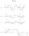
- Fig. 3 is a waveform chart showing signal waveforms corresponding to the respective portions of the circuit shown in Fig. 2.
- the circuit shown in Fig. 2 is substantially identical to the conventional noise reduction circuit shown in Fig. 1 except for provision of a waveform correcting circuit 8.
- a signal output from subtractor 3 formed of noise components and non-correlative luminance signal components is supplied to limiter 4 as well as to waveform correcting circuit 8.
- the signal waveform at the input (point A) of waveform correcting circuit 8 is schematically illustrated in Fig. 3 (A).
- each of a1 and a2 schematically indicates a situation wherein noise components are superimposed in the signal portion not having any change of the luminance signal in the vertical direction to be generated at the edge portion of an image.
- the input signal is applied to a limiter 8a as well as to the positive input of a subtractor 8b.
- the signal applied to limiter 8a has its amplitude limited, and the signal substantially consisting of the noise components is extracted to be applied to the negative input of subtractor 8b.
- the waveform at the negative input (point B) of subtractor 8b is schematically illustrated in Fig. 3 at (B).
- Fig. 3(B) each of a1' and a2' schematically indicates a situation wherein noise components are superimposed in the same manner as described above.
- a waveform output as schematically shown in Fig. 3 (C) is obtained from subtractor 8b, and the output is multiplied by K2 by a constant multiplying circuit 8c to be applied to one input of an adder 8d.
- the output of subtractor 6 is applied to the other input of adder 8d.
- the output of adder 8d is supplied to signal processing circuitry of reproduction system in the VCR through an output terminal 7.
- the luminance signal output from subtractor 6 lacking the non-correlative components has been given the non-correlative components.
- the luminance signal Y having the noise components removed and having its defect corresponding to the non-correlative components compensated for is output from output terminal 7.
- the above-described limiter 8a and subtractor 8b substantially constitute a signal detecting circuit for detecting a defect corresponding to the non-correlative components.
- waveform correcting circuit 8 in Fig. 2 the input signal at the point A is applied to the negative input of subtractor 8b through limiter 8a while it is applied directly to the positive input of subtractor 8b. A delay is made between the two input signals to subtractor 8b accordingly, thus producing distortion in an output signal from subtractor 8b.
- noise components a1''and a2'' superimposed in the signal portions not having any change of the luminance signal in the vertical direction result in flicker on the reproduced picture.
- Fig. 3(B') is a waveform chart with a waveform for one cycle in Fig. 3(B) enlarged, and distortion and deformation are seen in the amplitude-limited waveform.
- a waveform detecting circuit includes a first power supply for supplying a first reference potential, a first comparator for comparing an input signal and the first reference potential to determine the relation as to large or small therebetween, a first electronic switch for selectively supplying the input signal or the first reference potential based on the output of the first comparator, a second power supply for supplying a second reference potential, a second comparator for comparing the input signal and the second reference potential to determine the relation as to large or small therebetween, a second electronic switch for selectively supplying the input signal or the second reference potential, and an adder for adding up the outputs of the first and second electronic switches.
- Fig. 4 is a block diagram showing a noise reduction circuit including a waveform detecting circuit according to one embodiment of the present invention.
- Fig. 5 is a waveform chart showing signal waveforms corresponding to the respective portions of the embodiment shown in Fig. 4.
- the circuit shown in Fig. 4 is identical to the conventional noise reduction circuit shown in Fig. 2 except that a waveform correcting circuit 11 is provided in place of waveform correcting circuit 8 in Fig. 2. Therefore, a description will not be repeated on the portions identical to those in the circuit in Fig. 2.
- a signal output from subtractor 3 formed of noise components and non-correlative luminance components is applied to limiter 4 and waveform correcting circuit 11. More specifically stated, the applied signal is also applied to the positive input 12a of a differential comparator 12, the negative input 13b of a differential comparator 13, one fixed contact 14a of an electronic switch 14, and one fixed contact 15a of an electronic switch 15.
- a first reference potential V1 is applied to the negative input 12b of differential comparator 12 and the other fixed contact 14b of electronic switch 14.
- a second reference potential V2 is applied to the positive input 13a of differential comparator 13 and the other fixed contact 15b of electronic switch 15.
- the first and second reference potentials are opposite from each other in polarity and have absolute values equal to each other.
- differential comparator 12 is applied to a control contact 14d of electronic switch 14, and the output of differential comparator 13 is applied to a control contact 15d of electronic switch 15.
- Electronic switch 14 has its movable contact 14c connected to one input of an adder 16, and electronic switch 15 has its movable contact 15c connected to the other input of adder 16.
- the output of adder 16 is multiplied by K2 by a constant multiplying circuit 17 to be applied to one input of an adder 18.
- the output of subtractor 6 is applied to the other input of adder 18.
- the output of adder 18 is supplied to the reproduction system signal processing circuitry (not shown) of the VCR through output terminal 7.
- Fig. 5(a) The waveform of an input signal at the input (point a ) of waveform correcting circuit 11 is schematically illustrated in Fig. 5(a).
- the input signal is compared with the first reference potential V1 (Fig. 5(b)) by differential comparator 12, and differential comparator 12 outputs a control signal at an H level to be applied to the control contact 14d of electronic switch 14 during the period when the input signal is higher than the reference potential V1.
- movable contact 14c is connected to fixed contact 14a (H side), and the input signal at the point a is selected to be applied to one input of adder 16 as it is.
- differential comparator 12 outputs a control signal at an L level to be applied to the control contact 14d of electronic switch 14.
- movable contact 14c is connected to fixed contact 14b (L side), and the reference potential V1 is selected to be applied to one input of adder 16.
- V1 is selected to be applied to one input of adder 16.
- a signal of a waveform as shown in Fig. 5(d) is output from the fixed contact 14c of electronic switch 14.
- noise components indicated by a1 and a2 as shown in Fig. 5(a) are completely removed.
- the circuit formed of differential comparator 12 and electronic switch 14 as stated above will hereinafter be referred to as a first detection circuit 9.
- the input signal at the point a is compared with the second reference potential V2 (Fig. 5(c)) by differential comparator 13, and differential comparator 13 outputs a control signal at H level to be applied to the control contact 15d of electronic switch 15 during the period when the input signal is lower than the reference potential V2.
- movable contact 15c is connected to fix contact 15a (H side), and the input signal at the point a is selected to be applied to the other input of adder 16 as it is.
- differential comparator 13 outputs a control signal at L level to be applied to the control contact 15d of electronic switch 15.
- movable contact 15c is connected to fixed contact 15b (L side), and the reference potential V2 is selected to be applied to the other input of adder 16.
- V2 is selected to be applied to the other input of adder 16.
- a signal of a waveform as shown in Fig. 5(e) is output from the movable contact 15c of electronic switch 15.
- noise components indicated by a1 and a2 as shown in Fig. 5(a) are completely removed.
- the circuit formed of differential comparator 13 and electronic switch 15 as stated above will hereinafter be referred to as a second detection circuit 10.
- the outputs (Figs. 5(d) and (e)) of first and second detection circuits 9 and 10 are added up at adder 16, and a signal of a waveform as shown in Fig. 5(f) in which the reference potentials V1 and V2 are canceled out is output from adder 16.
- the signal portion significantly containing the noise components is canceled, a signal substantially constituting of the non-correlative portion of the luminance signal is obtained to be added by adder 18 to the luminance signal lacking the non-correlative components output from subtractor 6.
- the luminance signal Y having of the noise components removed and having its defect corrected is output from output terminal 7.
- Appropriate setting of the values of referential potentials V1 and V2 permits the waveforms of the outputs of the first and second detection circuits to be changed, and a signal in a desired range can be extracted as non-relative components.
- the above described first and second detection circuits as well as the adder 16 constitute a signal detecting circuit for detecting a defect corresponding to the non-correlative components.
- noise components in the signal portion not having any change of the luminance signal in the vertical direction are also removed completely.
- Fig. 6A illustrates an equivalent circuit of first detection circuit 9 in Fig. 4 being implemented as an integrated circuit formed of transistors, resistors and constant current sources
- Fig. 6B illustrates an equivalent circuit of second detection circuit 10 in Fig. 4 being implemented as a similar integrated circuit.
- the lower half represents a specific circuit configuration of differential comparator 12
- the upper half represents a specific circuit configuration of electronic switch 14.
- Differential comparator 12 applies a control signal to the control contact 14d of electronic switch 14 in response to the potential difference between positive input 12a and negative input 12b. Either one of the input signal at the point a or the reference potential V1 at the point b is selected in response to this control signal, and the selected one is output from movable contact 14c.
- the lower half represents a specific circuit configuration of differential comparator 13
- the upper half represents a specific circuit configuration of electronic switch 15.
- Differential comparator 13 applies a control signal to the control contact 15d of electronic switch 15 in response to the potential difference between positive input 13a and negative input 13b. Either one of the input signal at the point a or the reference potential V2 at the point c is selected in response to this control signal, and the selected one is output from movable contact 15c.
- distortion attributed to the delay of a signal or even-numbered order distortion are not made in an output signal from the waveform detecting circuit, and, therefore, adverse effects such as the hue lagging on a reproduced picture in the VCR can be prevented.
Landscapes
- Engineering & Computer Science (AREA)
- Multimedia (AREA)
- Signal Processing (AREA)
- Television Signal Processing For Recording (AREA)
- Picture Signal Circuits (AREA)
- Manipulation Of Pulses (AREA)
Abstract
Description
- The present invention relates generally to a waveform detecting circuit, and more specifically, to a waveform detecting circuit which detects a defect in a video information signal in a video equipment such as a video cassette recorder (hereinafter referred to as VCR).
- Generally, in a video equipment such as a VCR, a video information signal (for example, a luminance signal Y) usually has defects in various bands generated due to different causes, for example, when Y/C separation is performed by circuitry of recording system or noise reduction is conducted by circuitry of reproducing system.
- By way of illustrating an example of a defect in such a video information signal, a description will be provided on how a defect in the luminance signal Y is made by a noise reduction circuit for canceling the line noise of the luminance signal Y in circuitry of reproducing system in a VCR.
- Fig. 1 is a block diagram schematically showing a structure of such a conventional noise reduction circuit in the reproducing system circuitry in a VCR. Referring to Fig. 1, the luminance signal Y including noise components, reproduced from a magnetic tape by a reproduction circuit (not shown), is applied to a 1H delay circuit 2 (H represents one horizontal period) and to the positive inputs of
subtractors input terminal 1. The luminance signal containing the noise components delayed by 1H period through1H delay circuit 2 is applied to the negative input ofsubtractor 3. Then,subtractor 3 compares two luminance signals of two successive 1H periods and outputs a difference signal corresponding to the noise components. The difference signal has its amplitude limited by alimiter 4, and is increased by K times through a constant multiplyingcircuit 5 to be applied to the negative input ofsubtractor 6 as the noise components. Consequently,subtractor 6 subtracts the noise components from the luminance signal including the noise components supplied from the reproduction circuit, and the luminance signal Y whose noise components are canceled is output from anoutput terminal 7. - However, in the circuit shown in Fig. 1, the output of
subtractor 3 contains not only pure noise components but also non-correlative components between luminance signals of successive two lines. Subtraction of such non-correlative components together with the noise components from the luminance signal Y bysubtractor 6 results in a defect in the luminance signal Y corresponding to the above-stated non-correlative components. Such a defect in a video information signal degrades the frequency characteristics and S/N ratio in the entire VCR and must therefore be compensated for by some method. - Fig. 2 is a block diagram schematically showing a conventional noise reduction circuit including a waveform correcting circuit for compensating for such a defect in a video information signal, and Fig. 3 is a waveform chart showing signal waveforms corresponding to the respective portions of the circuit shown in Fig. 2. The circuit shown in Fig. 2 is substantially identical to the conventional noise reduction circuit shown in Fig. 1 except for provision of a
waveform correcting circuit 8. - More specifically stated, a signal output from
subtractor 3 formed of noise components and non-correlative luminance signal components is supplied to limiter 4 as well as to waveformcorrecting circuit 8. The signal waveform at the input (point A) ofwaveform correcting circuit 8 is schematically illustrated in Fig. 3 (A). In Fig. 3(A), each of a₁ and a₂ schematically indicates a situation wherein noise components are superimposed in the signal portion not having any change of the luminance signal in the vertical direction to be generated at the edge portion of an image. The input signal is applied to a limiter 8a as well as to the positive input of asubtractor 8b. The signal applied to limiter 8a has its amplitude limited, and the signal substantially consisting of the noise components is extracted to be applied to the negative input ofsubtractor 8b. The waveform at the negative input (point B) ofsubtractor 8b is schematically illustrated in Fig. 3 at (B). In Fig. 3(B), each of a₁' and a₂' schematically indicates a situation wherein noise components are superimposed in the same manner as described above. - A waveform output as schematically shown in Fig. 3 (C) is obtained from
subtractor 8b, and the output is multiplied by K2 by a constant multiplyingcircuit 8c to be applied to one input of an adder 8d. The output ofsubtractor 6 is applied to the other input of adder 8d. The output of adder 8d is supplied to signal processing circuitry of reproduction system in the VCR through anoutput terminal 7. - Then, from the input signal (Fig. 3(A)) applied to
waveform correcting circuit 8 fromsubtractor 3, the signal (Fig. 3(B)) mainly consisting of the noise components is canceled, andsubtractor 8b outputs a signal (Fig. 3(C)) mainly formed of the non-correlative components of the luminance signal. In Fig. 3(c), each of a₁''and a₂'' schematically indicates a situation wherein noise components are superimposed in the same manner as described above. - More specifically, the luminance signal output from
subtractor 6 lacking the non-correlative components has been given the non-correlative components. As a result, the luminance signal Y having the noise components removed and having its defect corresponding to the non-correlative components compensated for is output fromoutput terminal 7. In thewaveform correcting circuit 8, the above-described limiter 8a andsubtractor 8b substantially constitute a signal detecting circuit for detecting a defect corresponding to the non-correlative components. - In
waveform correcting circuit 8 in Fig. 2, the input signal at the point A is applied to the negative input ofsubtractor 8b through limiter 8a while it is applied directly to the positive input ofsubtractor 8b. A delay is made between the two input signals tosubtractor 8b accordingly, thus producing distortion in an output signal fromsubtractor 8b. - In addition, the noise components a₁''and a₂'' superimposed in the signal portions not having any change of the luminance signal in the vertical direction result in flicker on the reproduced picture.
- Also, when a differential limiter circuit is used for limiter 8a, even-numbered order distortion incidental to the principle of the operation of the differential limiter circuit is generated in an output signal. Fig. 3(B') is a waveform chart with a waveform for one cycle in Fig. 3(B) enlarged, and distortion and deformation are seen in the amplitude-limited waveform.
- When the output of limiter 8a including such signal distortion is processed at various video signal processing circuits, an adverse effect such as the hue lagging from the original on a reproduced picture, thereby degrading the performance of the VCR.
- It is therefore a main object of the present invention to provide a waveform detecting circuit capable of preventing the degradation of the picture quality of a reproduced picture due to video information signal distortion in a video equipment.
- A waveform detecting circuit according to the present invention, if shortly stated, includes a first power supply for supplying a first reference potential, a first comparator for comparing an input signal and the first reference potential to determine the relation as to large or small therebetween, a first electronic switch for selectively supplying the input signal or the first reference potential based on the output of the first comparator, a second power supply for supplying a second reference potential, a second comparator for comparing the input signal and the second reference potential to determine the relation as to large or small therebetween, a second electronic switch for selectively supplying the input signal or the second reference potential, and an adder for adding up the outputs of the first and second electronic switches.
- It is therefore a main advantage brought about by the present invention that deterioration of a video information signal due to signal delay and even-numbered order distortion can be prevented in a waveform correcting circuit.
- The foregoing and other objects, features, aspects and advantages of the present invention will become more apparent from the following detailed description of the present invention when taken in conjunction with the accompanying drawings.
-
- Fig. 1 is a block diagram schematically showing a conventional noise reduction circuit;
- Fig. 2 is a block diagram schematically showing another conventional noise reduction circuit;
- Fig. 3 is a waveform chart for illustrating the operation of the conventional noise reduction circuit shown in Fig. 2;
- Fig. 4 is a block diagram showing a noise reduction circuit including a waveform detecting circuit according to one embodiment of the present invention;
- Fig. 5 is a waveform chart for illustrating the operation of the embodiment shown in Fig. 4; and
- Figs. 6A and 6B are diagrams each showing an equivalent circuit of the waveform detecting circuit shown in Fig. 4 being implemented as an integrated circuit.
- Fig. 4 is a block diagram showing a noise reduction circuit including a waveform detecting circuit according to one embodiment of the present invention. Fig. 5 is a waveform chart showing signal waveforms corresponding to the respective portions of the embodiment shown in Fig. 4.
- The circuit shown in Fig. 4 is identical to the conventional noise reduction circuit shown in Fig. 2 except that a
waveform correcting circuit 11 is provided in place ofwaveform correcting circuit 8 in Fig. 2. Therefore, a description will not be repeated on the portions identical to those in the circuit in Fig. 2. - Referring to Fig. 4, a signal output from
subtractor 3 formed of noise components and non-correlative luminance components is applied to limiter 4 andwaveform correcting circuit 11. More specifically stated, the applied signal is also applied to thepositive input 12a of adifferential comparator 12, thenegative input 13b of adifferential comparator 13, onefixed contact 14a of anelectronic switch 14, and one fixed contact 15a of anelectronic switch 15. - A first reference potential V₁ is applied to the
negative input 12b ofdifferential comparator 12 and the other fixedcontact 14b ofelectronic switch 14. A second reference potential V₂ is applied to the positive input 13a ofdifferential comparator 13 and the other fixedcontact 15b ofelectronic switch 15. The first and second reference potentials are opposite from each other in polarity and have absolute values equal to each other. - The output of
differential comparator 12 is applied to acontrol contact 14d ofelectronic switch 14, and the output ofdifferential comparator 13 is applied to acontrol contact 15d ofelectronic switch 15.Electronic switch 14 has itsmovable contact 14c connected to one input of anadder 16, andelectronic switch 15 has itsmovable contact 15c connected to the other input ofadder 16. - The output of
adder 16 is multiplied by K2 by a constant multiplyingcircuit 17 to be applied to one input of anadder 18. The output ofsubtractor 6 is applied to the other input ofadder 18. The output ofadder 18 is supplied to the reproduction system signal processing circuitry (not shown) of the VCR throughoutput terminal 7. - Referring to Figs. 4 and 5, the operation of one embodiment according to the present invention will be described. The waveform of an input signal at the input (point a) of
waveform correcting circuit 11 is schematically illustrated in Fig. 5(a). The input signal is compared with the first reference potential V₁ (Fig. 5(b)) bydifferential comparator 12, anddifferential comparator 12 outputs a control signal at an H level to be applied to thecontrol contact 14d ofelectronic switch 14 during the period when the input signal is higher than the reference potential V₁. During the period of this control signal being applied,movable contact 14c is connected to fixedcontact 14a (H side), and the input signal at the point a is selected to be applied to one input ofadder 16 as it is. During the period when the input signal is lower than the reference potential V₁,differential comparator 12 outputs a control signal at an L level to be applied to thecontrol contact 14d ofelectronic switch 14. During the period of this control signal being applied,movable contact 14c is connected to fixedcontact 14b (L side), and the reference potential V₁ is selected to be applied to one input ofadder 16. In other words, a signal of a waveform as shown in Fig. 5(d) is output from the fixedcontact 14c ofelectronic switch 14. In Fig. 5(d), noise components indicated by a₁ and a₂ as shown in Fig. 5(a) are completely removed. The circuit formed ofdifferential comparator 12 andelectronic switch 14 as stated above will hereinafter be referred to as afirst detection circuit 9. - The input signal at the point a is compared with the second reference potential V₂ (Fig. 5(c)) by
differential comparator 13, anddifferential comparator 13 outputs a control signal at H level to be applied to thecontrol contact 15d ofelectronic switch 15 during the period when the input signal is lower than the reference potential V₂. During the period of this control signal being applied,movable contact 15c is connected to fix contact 15a (H side), and the input signal at the point a is selected to be applied to the other input ofadder 16 as it is. During the period when the input signal is higher than the reference potential V₂,differential comparator 13 outputs a control signal at L level to be applied to thecontrol contact 15d ofelectronic switch 15. During the period of this control signal being applied,movable contact 15c is connected to fixedcontact 15b (L side), and the reference potential V₂ is selected to be applied to the other input ofadder 16. In other words, a signal of a waveform as shown in Fig. 5(e) is output from themovable contact 15c ofelectronic switch 15. In Fig. 5(e), noise components indicated by a₁ and a₂ as shown in Fig. 5(a) are completely removed. The circuit formed ofdifferential comparator 13 andelectronic switch 15 as stated above will hereinafter be referred to as asecond detection circuit 10. - The outputs (Figs. 5(d) and (e)) of first and
second detection circuits adder 16, and a signal of a waveform as shown in Fig. 5(f) in which the reference potentials V₁ and V₂ are canceled out is output fromadder 16. In other words, the signal portion significantly containing the noise components is canceled, a signal substantially constituting of the non-correlative portion of the luminance signal is obtained to be added byadder 18 to the luminance signal lacking the non-correlative components output fromsubtractor 6. As a result, the luminance signal Y having of the noise components removed and having its defect corrected is output fromoutput terminal 7. Appropriate setting of the values of referential potentials V₁ and V₂ permits the waveforms of the outputs of the first and second detection circuits to be changed, and a signal in a desired range can be extracted as non-relative components. - Accordingly, in the
waveform correcting circuit 11, the above described first and second detection circuits as well as theadder 16 constitute a signal detecting circuit for detecting a defect corresponding to the non-correlative components. - In comparison of
waveform correcting circuit 11 in Fig. 4 and the conventionalwaveform correcting circuit 8 in Fig. 2, it is noted that no signal delay is made between a signal throughdifferential comparator 12 and a signal throughdifferential comparator 13 in the circuit in Fig. 4, and, therefore, distortion caused by a signal delay as in the case of the conventional example will not be produced in an output signal from the waveform detecting circuit. No even-numbered order distortion will be generated in an output signal from the waveform detecting circuit, because an electronic switch is used in place of a differential limiter such as limiter 8a in Fig. 2. - In addition, noise components in the signal portion not having any change of the luminance signal in the vertical direction are also removed completely.
- Fig. 6A illustrates an equivalent circuit of
first detection circuit 9 in Fig. 4 being implemented as an integrated circuit formed of transistors, resistors and constant current sources, and Fig. 6B illustrates an equivalent circuit ofsecond detection circuit 10 in Fig. 4 being implemented as a similar integrated circuit. - In Fig. 6A, the lower half represents a specific circuit configuration of
differential comparator 12, and the upper half represents a specific circuit configuration ofelectronic switch 14.Differential comparator 12 applies a control signal to thecontrol contact 14d ofelectronic switch 14 in response to the potential difference betweenpositive input 12a andnegative input 12b. Either one of the input signal at the point a or the reference potential V₁ at the point b is selected in response to this control signal, and the selected one is output frommovable contact 14c. - In Fig. 6B, the lower half represents a specific circuit configuration of
differential comparator 13, and the upper half represents a specific circuit configuration ofelectronic switch 15.Differential comparator 13 applies a control signal to thecontrol contact 15d ofelectronic switch 15 in response to the potential difference between positive input 13a andnegative input 13b. Either one of the input signal at the point a or the reference potential V₂ at the point c is selected in response to this control signal, and the selected one is output frommovable contact 15c. - As stated above, according to the embodiment of the present invention, distortion attributed to the delay of a signal or even-numbered order distortion are not made in an output signal from the waveform detecting circuit, and, therefore, adverse effects such as the hue lagging on a reproduced picture in the VCR can be prevented.
- Although in the above-described embodiment, the cases have been described in which the present invention is applied to a noise reduction circuit of reproducing system in a VCR, similar effects can be provided by applying the invention to various circuits in video equipment such as a Y/C separation circuit of recording system in a VCR.
- Although the present invention has been described and illustrated in detail, it is clearly understood that the same is by way of illustration and example only and is not to be taken by way of limitation, the spirit and scope of the present invention being limited only by the terms of the appended claims.
Claims (3)
- A circuit for detecting the waveform of an input signal, comprising:
first power supply means for supplying a first reference potential (V₁);
first comparison means (12) for comparing said input signal and said first reference potential to determine the relation as to large or small therebetween;
first electronic switch means (14) responsive to the output of said first comparison means for selectively supplying said input signal or said first reference potential;
second power supply means for supplying a second reference potential (V₂);
second comparison means (13) for comparing said input signal and said second reference potential to determine the relation as to large or small therebetween;
second electronic switch means (15) responsive to the output of said second comparison means for selectively supplying said input signal or said second reference potential; and
addition means (16) for adding up the outputs of said first and second electronic switch means. - A waveform detecting circuit according to claim 1, wherein
said first and second reference potentials have positive and negative polarities, respectively, and absolute values equal to each other,
said input signal and said first reference potential are applied to the positive and negative inputs of said first comparison means, and
said input signal and said second reference potential are applied to the negative and positive inputs of the second comparison means. - A waveform detecting circuit according to claim 2, wherein
said first electronic switch means selects said input signal during the period when said input signal is higher than said first reference potential and otherwise selects said first reference potential, and
said second electronic switch means selects said input signal during the period when said input signal is lower than said second reference potential and otherwise selects said second reference potential.
Applications Claiming Priority (2)
| Application Number | Priority Date | Filing Date | Title |
|---|---|---|---|
| JP404320/90 | 1990-12-20 | ||
| JP40432090 | 1990-12-20 |
Publications (3)
| Publication Number | Publication Date |
|---|---|
| EP0492462A2 true EP0492462A2 (en) | 1992-07-01 |
| EP0492462A3 EP0492462A3 (en) | 1992-11-25 |
| EP0492462B1 EP0492462B1 (en) | 1996-03-06 |
Family
ID=18513997
Family Applications (1)
| Application Number | Title | Priority Date | Filing Date |
|---|---|---|---|
| EP91121840A Expired - Lifetime EP0492462B1 (en) | 1990-12-20 | 1991-12-19 | Waveform detecting circuit |
Country Status (3)
| Country | Link |
|---|---|
| EP (1) | EP0492462B1 (en) |
| JP (1) | JP2698263B2 (en) |
| DE (1) | DE69117700T2 (en) |
Citations (4)
| Publication number | Priority date | Publication date | Assignee | Title |
|---|---|---|---|---|
| JPS5593377A (en) * | 1979-01-10 | 1980-07-15 | Matsushita Electric Ind Co Ltd | Sn ratio improving unit |
| GB2085690A (en) * | 1980-09-30 | 1982-04-28 | Sony Corp | Periodic pulse forming circuit |
| EP0169052A2 (en) * | 1984-07-13 | 1986-01-22 | Victor Company Of Japan, Limited | Noise reduction circuit for video signal |
| JPS61234176A (en) * | 1985-04-09 | 1986-10-18 | Matsushita Electric Ind Co Ltd | Noise lowering circuit |
Family Cites Families (2)
| Publication number | Priority date | Publication date | Assignee | Title |
|---|---|---|---|---|
| JPS5921463B2 (en) * | 1978-08-18 | 1984-05-19 | 松下電器産業株式会社 | heating/cooling machine |
| JPS6038945A (en) * | 1983-08-11 | 1985-02-28 | Fujitsu Ltd | Fuel wave rectifier circuit |
-
1991
- 1991-12-16 JP JP3331944A patent/JP2698263B2/en not_active Expired - Fee Related
- 1991-12-19 EP EP91121840A patent/EP0492462B1/en not_active Expired - Lifetime
- 1991-12-19 DE DE1991617700 patent/DE69117700T2/en not_active Expired - Fee Related
Patent Citations (4)
| Publication number | Priority date | Publication date | Assignee | Title |
|---|---|---|---|---|
| JPS5593377A (en) * | 1979-01-10 | 1980-07-15 | Matsushita Electric Ind Co Ltd | Sn ratio improving unit |
| GB2085690A (en) * | 1980-09-30 | 1982-04-28 | Sony Corp | Periodic pulse forming circuit |
| EP0169052A2 (en) * | 1984-07-13 | 1986-01-22 | Victor Company Of Japan, Limited | Noise reduction circuit for video signal |
| JPS61234176A (en) * | 1985-04-09 | 1986-10-18 | Matsushita Electric Ind Co Ltd | Noise lowering circuit |
Non-Patent Citations (1)
| Title |
|---|
| K.B.Benson, Television Engineering Handbook, 1986, McGraw-Hill, pages 13.138 - 13.141 * |
Also Published As
| Publication number | Publication date |
|---|---|
| EP0492462B1 (en) | 1996-03-06 |
| DE69117700T2 (en) | 1996-08-08 |
| JPH0567952A (en) | 1993-03-19 |
| DE69117700D1 (en) | 1996-04-11 |
| EP0492462A3 (en) | 1992-11-25 |
| JP2698263B2 (en) | 1998-01-19 |
Similar Documents
| Publication | Publication Date | Title |
|---|---|---|
| US4807034A (en) | Noise reduction circuit for video signal having field memory | |
| JPH0720265B2 (en) | Video signal processing circuit | |
| KR0160529B1 (en) | Video motion detector circuit with full band response except for diagonal spatial frequencies | |
| JPH06311527A (en) | Adaptive picture peaking circuit using cross fader | |
| JPH04280595A (en) | Patter adaptive type digital comb-like filter for separating brightness signal from color signal | |
| JPS6345151B2 (en) | ||
| US4703343A (en) | Noise reduction feedback type comb filter | |
| US5105274A (en) | Circuits for reducing noise in a video signal | |
| EP0492462B1 (en) | Waveform detecting circuit | |
| JP2951443B2 (en) | Motion signal detection circuit | |
| JPH0427287A (en) | Drop-out compensating circuit | |
| JP2798562B2 (en) | Signal correction circuit | |
| JPH1093990A (en) | Automatic gain control loop circuit | |
| JPS58123284A (en) | Compensating circuit for still picture signal | |
| JPS62290268A (en) | Noise eliminator | |
| JP2812271B2 (en) | Video non-additive mixing device | |
| JP3013484B2 (en) | Video signal playback device | |
| JP3128331B2 (en) | Reproduction color signal processing circuit | |
| KR0132501B1 (en) | Image quality compensation apparatus by using twin head | |
| JPH05160672A (en) | Cyclic comb-line filter | |
| JPH03261211A (en) | Three-line comb-line filter | |
| JPH0683483B2 (en) | Comb filter | |
| JPS62281681A (en) | Cycice type noise reducing device | |
| JPS5937788A (en) | Line correlation and dropout compensating circuit | |
| JPH0738728B2 (en) | Video signal playback device |
Legal Events
| Date | Code | Title | Description |
|---|---|---|---|
| PUAI | Public reference made under article 153(3) epc to a published international application that has entered the european phase |
Free format text: ORIGINAL CODE: 0009012 |
|
| AK | Designated contracting states |
Kind code of ref document: A2 Designated state(s): DE FR |
|
| PUAL | Search report despatched |
Free format text: ORIGINAL CODE: 0009013 |
|
| AK | Designated contracting states |
Kind code of ref document: A3 Designated state(s): DE FR |
|
| 17P | Request for examination filed |
Effective date: 19921117 |
|
| 17Q | First examination report despatched |
Effective date: 19941004 |
|
| GRAA | (expected) grant |
Free format text: ORIGINAL CODE: 0009210 |
|
| AK | Designated contracting states |
Kind code of ref document: B1 Designated state(s): DE FR |
|
| REF | Corresponds to: |
Ref document number: 69117700 Country of ref document: DE Date of ref document: 19960411 |
|
| ET | Fr: translation filed | ||
| PLBE | No opposition filed within time limit |
Free format text: ORIGINAL CODE: 0009261 |
|
| STAA | Information on the status of an ep patent application or granted ep patent |
Free format text: STATUS: NO OPPOSITION FILED WITHIN TIME LIMIT |
|
| 26N | No opposition filed | ||
| PGFP | Annual fee paid to national office [announced via postgrant information from national office to epo] |
Ref country code: FR Payment date: 20071210 Year of fee payment: 17 |
|
| PGFP | Annual fee paid to national office [announced via postgrant information from national office to epo] |
Ref country code: DE Payment date: 20071213 Year of fee payment: 17 |
|
| REG | Reference to a national code |
Ref country code: FR Ref legal event code: ST Effective date: 20090831 |
|
| PG25 | Lapsed in a contracting state [announced via postgrant information from national office to epo] |
Ref country code: DE Free format text: LAPSE BECAUSE OF NON-PAYMENT OF DUE FEES Effective date: 20090701 |
|
| PG25 | Lapsed in a contracting state [announced via postgrant information from national office to epo] |
Ref country code: FR Free format text: LAPSE BECAUSE OF NON-PAYMENT OF DUE FEES Effective date: 20081231 |