EP0491973B1 - Integrated pneumatically and electrostatically controlled scanning tunneling microscope and method of making the same - Google Patents
Integrated pneumatically and electrostatically controlled scanning tunneling microscope and method of making the same Download PDFInfo
- Publication number
- EP0491973B1 EP0491973B1 EP90125214A EP90125214A EP0491973B1 EP 0491973 B1 EP0491973 B1 EP 0491973B1 EP 90125214 A EP90125214 A EP 90125214A EP 90125214 A EP90125214 A EP 90125214A EP 0491973 B1 EP0491973 B1 EP 0491973B1
- Authority
- EP
- European Patent Office
- Prior art keywords
- tip
- membrane
- substrate
- electrodes
- etching
- Prior art date
- Legal status (The legal status is an assumption and is not a legal conclusion. Google has not performed a legal analysis and makes no representation as to the accuracy of the status listed.)
- Expired - Lifetime
Links
Images


Classifications
-
- G—PHYSICS
- G01—MEASURING; TESTING
- G01Q—SCANNING-PROBE TECHNIQUES OR APPARATUS; APPLICATIONS OF SCANNING-PROBE TECHNIQUES, e.g. SCANNING PROBE MICROSCOPY [SPM]
- G01Q10/00—Scanning or positioning arrangements, i.e. arrangements for actively controlling the movement or position of the probe
- G01Q10/02—Coarse scanning or positioning
-
- G—PHYSICS
- G01—MEASURING; TESTING
- G01Q—SCANNING-PROBE TECHNIQUES OR APPARATUS; APPLICATIONS OF SCANNING-PROBE TECHNIQUES, e.g. SCANNING PROBE MICROSCOPY [SPM]
- G01Q10/00—Scanning or positioning arrangements, i.e. arrangements for actively controlling the movement or position of the probe
- G01Q10/04—Fine scanning or positioning
-
- G—PHYSICS
- G01—MEASURING; TESTING
- G01Q—SCANNING-PROBE TECHNIQUES OR APPARATUS; APPLICATIONS OF SCANNING-PROBE TECHNIQUES, e.g. SCANNING PROBE MICROSCOPY [SPM]
- G01Q60/00—Particular types of SPM [Scanning Probe Microscopy] or microscopes; Essential components thereof
- G01Q60/10—STM [Scanning Tunnelling Microscopy] or apparatus therefor, e.g. STM probes
- G01Q60/16—Probes, their manufacture, or their related instrumentation, e.g. holders
Definitions
- the invention relates to a method of forming an integrated scanning tunneling microscope, and more particularly, to a pneumatically and electrostatically driven version of same.
- a scanning tunneling microscope scans over the surface of a sample with a conductive tip in very close relation to a conductive surface, i. e. within the space of the diameters of several atoms (approximately within 0.5 nm). Under these conditions a tunneling current flows between the tip and the surface, that is, the probability density function of electrons for atoms in the tip overlaps in space the probability density function of electrons for atoms on the surface. As a result, tunneling occurs in the form of electron current flow between the tip and the surface if a suitable bias voltage between these two conductors is applied. Typically, for a tip to sample spacing of a few nm 100 millivolts of bias voltage will provide 1 nanoampere of current.
- This tripod consists of 3 piezoelectric rods of material joined at a junction; each rod expands and contracts along one of 3 Cartesian coordinate axes.
- the tip is mounted at the junction of the 3 rods. The tip is brought into proximity of the surface by a rough positioner. Thereafter the piezoelectric tripods are used to scan the tip across the surface to develop an image of that surface.
- the electric fields caused by the control voltages cause the piezoelectric bimorphs to move in any desired fashion within ranges determined by the design.
- the bimorph cantilevers have tips with very sharp points formed thereon by evaporation deposition of a conductive material through a shadow mask. The tips are moved by the action of the control circuit and the piezoelectric bimorphs so to stay within a very small distance of a conducting surface. All STMs controlled by piezoelectric materials have the disadvantage of having a hysteresis effect which is not ideal for a high absolute accuracy.
- a protruding tip is formed on the center portion which is capable of being moved in the Z direction by means of electrostatic forces. It would be extremely difficult to successfully fabricate the integrated STM described in the European Patent cited above. Furthermore, the integrated STM is fabricated from one piece of material in a way that the X, Y and Z movements are not decoupled from each other and are therefore not ideal for tip movement with maximum accuracy.
- the invention also comprises two preferred processes for fabricating scanning tunneling microscopes in accordance with the invention.
- Fig. 1 depicts a scanning tunneling microscope system.
- a conductive surface (1) having topographical features (2) and (4) etc. is scanned by a conductive tip (6).
- This tip is very narrow at its point, and preferably terminates in a single atom at the point (8).
- the point (8) is scanned over the conductive surface (1) by an electrostatic transducer (10) by defining a plurality of raster scan lines in the X-Y plane.
- the transducer (10) also moves the tip back and forth along Z axis as the tip is scanned in the X-Y plane so as to maintain a relatively constant distance between the tip point (8) and the uppermost portion of the topographical feature over which the tip is scanned.
- This distance is usually around 0.1 to 1 nm, and must be within the overlap region of the probability density functions of the electrons for the atoms of the tip and the atoms in the uppermost regions of the topographical feature over which the tip currently scans.
- a tunneling current which is symbolized by the arrow I T will flow between the tip point (8) and the conductive surface.
- the magnitude of the tunneling current I T is exponentially related to the distance between the tip and the surface.
- the bias voltage is applied between the tip (6) and the conductive surface (1) by a bias voltage source (12).
- a current sensor (14) senses the magnitude of the tunneling current I T and outputs a feedback signal on line (16) which is proportional to the magnitude of the tunneling current.
- a feedback circuit control system (18) receives this feedback signal and generates suitable electrostatic transducer driving signals on the bus (20) to cause the electrostatic transducer to move the tip (6) in such a manner that the tunneling current I T is maintained at a relatively constant value.
- the control system (18) also generates suitable electrostatic transducer driving signals on the bus (20) to cause the tip (6) to be raster scanned across the conductive surface (1).
- Fig. 2A shows mechanical details of a scanning tunneling structure according to the teachings of the invention.
- This STM is suitable for the electrostatic X-Y-Z deflection as previously described.
- the bottom side of a thin membrane (24) holds the STM tip (25).
- a metallic coating (29) is applied to the tip (25) and to a part of silicon frame (21).
- a preferred coating for this purpose is a platinum coating with a thickness of about 0.1 ⁇ m.
- the membrane is intimately fixed to glass block (30) by silicon frame (21).
- the top side of the membrane (24) is several ⁇ m below the frame surface.
- Two pairs of metallic electrodes X1, X2, Y1, Y2 are arranged on glass block (30).
- the electrode thickness is in the range of about 0.1 to 1 ⁇ m, and preferably of about 1 ⁇ m.
- Glass block (30) which is typically several mm thick is provided with bores (23).
- the bores (23) may have the form of slots as shown in the top plan view of Fig. 2 B.
- End pieces (32) shown in Fig. 2A which are fixed to glass block (30) via gaskets (31) form part of a pressure generating chamber (not shown).
- This chamber can also be a vacuum chamber creating a pressure below one atmosphere which moves the membrane with the tip against the glass block.
- the membrane/tip assembly There are a number of technical requirements for the membrane/tip assembly which include the membrane stress and the eigenfrequency f o of the membrane.
- the membrane stiffness is neglectable for thin membranes.
- the membrane's damping can be specifically controlled as a function of the geometry of the environment, for example as a function of the bore diameter in glass block (30).
- the entire STM (including the tip) is advanced to within several ⁇ m of the sample surface to be studied using, for example, optical control means.
- the distance between tip and sample is controlled as a function of the U z -voltage.
- the maximum K-Y-scan is primarily dependent on the geometry of the STM-arrangement (membrane size, length of the tip etc.). If, for example, the tip length l is half the membrane side length a, then the maximum X-deflection equals the Z-deflection.
- the membrane is square-shaped with a side length a.
- the breakdown strength in a conventional electric actuator with an air gap is limited to approximately 3 X 10⁶ V/m by the electrical breakdown of air. For 200 V and a 10 ⁇ m gap, a breakdown strength of 2 X 10⁷ V/m is already obtained.
- a first process comprising several steps for making an integrated scanning tunneling microscope using pneumatic and electrostatic control of tip motion in Z-direction and electrostatic control of X- and Y-scan of the tip.
- Fabrication starts with a substrate (31, Fig. 3A).
- this substrate is silicon or some other substrate suitable for forming integrated electronic circuits.
- the first step in the fabrication sequence is to deposit silicon dioxide layers (32) on either side of the substrate (31). Silicon nitride layers can also be used.
- a pit of several ⁇ m depth is wet- or dry-etched into the front silicon dioxide layer (32) and into substrate (31) using for example buffered hydrofluoric acid for silicon dioxide and 37.5 % b. w.
- aqueous KOH for a silicon substrate The size corresponds to the future membrane size (say, 2mm side length).
- the remaining silicon dioxide layer on the front side is then removed.
- the flat fine-etched pit is covered with a resistent mask (33, Fig. 3B).
- a resistent mask for example, silicon dioxide or aluminum can be used as mask materials.
- An opening is provided in masking layer (33) in the center of the pit, followed by etching a hole through the substrate (31, Fig. 3C). This etching step may be a dry-etching step using chlorine or bromine chemistry.
- the mask (33) is removed, and the front side including the deep hole is covered with a tensile stressed film (34).
- the film material which preferably is silicon carbide or silicon nitride is deposited by plasma enhanced chemical vapor deposition.
- the film thickness is, for example, 2 ⁇ m.
- the hole may have a diameter which is noticeably above 2 ⁇ m, depending upon the etch process, so that only the sidewalls and the bottom of the hole are covered with the film material. As a result, the future tip will be hollow, which seems appropriate for weight reasons (Fig. 3D).
- Two pairs of metallic electrodes X1, X2, Y1 and Y2 (37, 38) are formed on glass block (40) by vapor deposition of Au or Al (Fig. 3F) using a molybdenum aperture mask.
- the dimensions of glass block (40) may be, for example, 3x3x2 mm.
- glass block (40) is provided with bores (43) which allow a pneumatical coarse approach of tip (35) in Z direction.
- glass block (40) is bonded to the silicon frame (31, 34) with X, Y electrodes (37, 38) being positioned above Z electrode (36) on membrane (34) and membrane (34) with Z electrode being arranged on a lower plane. Bonding is "mallory” bonding effected at about 300 °C and 1000 V. Proof of the bonding between glass block and substrate could be established by means of the SiC intermediate layer (Fig. 3G).
- the tip (35) does not protrude from its surrounding silicon frame (31), the remaining silicon dioxide mask (32) on the back side is removed and the frame is thinned by etching.
- the membrane material is an insulator, the tip (35) and a part of the membrane (34) and of silicon frame (31) on the bottom side have to be provided with an electrically conductive layer (39, Fig. 3G) to obtain voltage for the tunnel current.
- a preferred material for this layer is platinum which is applied with a thickness of about 0.1 ⁇ m.
- the deep hole (Fig. 3C) whose imprint forms the future tip (35) may be produced to have a diameter of 20 to 100 ⁇ m.
- the hole would have to be closed in part or in full by the following additional steps.
- the silicon carbide or silicon nitride deposition step (34, Fig. 3D) the hole is filled with a polymeric material, preferably with polyimide, and planarized.
- a second silicon carbide or silicon nitride layer is applied (not shown).
- This second silicon carbide or silicon nitride layer over the filled hole is partially opened in a reactive ion etching step, using a suitable mask such as a molybdenum mask with a lattice structure.
- a suitable mask such as a molybdenum mask with a lattice structure.
- oxygen plasma etching step the polyimide is removed from the tip for weight reasons. This step yields a lattice spanning the hole, which does not allow a release of the membrane tension during scanning later on. It is assumed however that given a reasonably small hole with a diameter ⁇ 50 ⁇ m, such a supporting structure will not be required.
- FIGs. 4A to 4E there is shown a second process comprising a planar technology for making an integrated scanning tunneling microscope.
- a layer of a conductive material for example a 0.1 ⁇ m platinum layer, is applied to a substrate (41) by vapor deposition using a molybdenum aperture mask thereby obtaining four quadrants (42A, 42B, Fig. 4A) which are later on used as the lower electrodes for the X, Y and Z motion of the tip.
- the substrate is silicon or some other substrate material suitable for forming integrated electronic circuits.
- a silicon dioxide layer (44) is applied to the surface of the electrodes (42A, 42B) overlapping said electrodes for example by plasma enhanced chemical vapor deposition. This silicon dioxide layer with a thickness in the range of about 2 to 5 ⁇ m serves as a spacer layer between the lower and upper electrodes and will be removed later on by selective etching to space the electrodes.
- annular metal conductor (45) for example a 0.1 ⁇ m platinum conductor, is applied to silicon dioxide layer (44) by vapor deposition using a molybdenum aperture mask.
- This annular metal conductor which covers approximately the same area as the lower electrodes (42A, 42B) forms the common counter-electrode for the four quadrant electrodes.
- a hole is provided in the center of the circular sandwich by reactive ion etching, followed by reactive ion etching of a tapered hole (47) through the silicon substrate (41), or of an inverted pyramid by anisotropic wet etching with for example 37.5 % b. w. aqueous KOH.
- This hole which extends nearly through the entire silicon wafer (41) forms a negative of the future tip which will be filled with the tunnel contact material and which is separated from the lower electrodes.
- the sandwich including the deep hole is covered with the tunnel contact material (48), for example with a 0.1 ⁇ m platinum layer, which deposited by vapor deposition using a molybdenum aperture mask.
- the tunnel current is fed through the conductor thus formed from the tip to the sample.
- a dielectric layer (49) of silicon carbide or silicon nitride is applied, using for example plasma enhanced chemical vapor deposition. The thickness of this layer may be 2 ⁇ m.
- This layer represents the oscillating membrane (49) to which the upper electrode (45) is connected by dielectric layer (46) and conductor (48, Fig. 4D).
- the silicon surrounding the tip is removed, for example by etching with an aqueous solution of 37.5 % b. w. KOH. Subsequently, the whole wafer is slightly thinned around the 3 studs (50) using the same solution. By means of these studs the scanning tunneling microscope is positioned on the substrate to be investigated.
- the silicon dioxide layer (44) between the electrodes (42A, 42B and 45) is completely removed by etching with buffered hydrofluoric acid. This provides a clearance space for the membrane for moving along the H, Y and Z axes when electric fields are applied to the electrodes.
- the platinum-silicon carbide tip is connected to the membrane and can freely be moved by the same.
- a glass block may be arranged to allow pneumatical coarse approach of the membrane/tip assembly along Z-axis (not shown).
- a cavity is provided between the membrane (49) and the glass block to allow oscillation of the membrane.
- the glass block may be perforated for varying the damping of the membrane by subjecting the membrane to pressure, or, the cavity between the glass block and the membrane may be evacuated before bonding, with the bonding being used to obtain a vacuum-tight sealing.
- the scanning tunneling microscope according to this invention are the hysteresis-free X-Y-Z drive and the high mechanical and thermal stability of the sensor head resulting from its low mass and small dimensions. As a result the arrangement is little susceptible to external vibrations. Control circuitry for the current supply for the distance control of the tip is integrated on the same semiconductor substrate. Furthermore, the signals resulting from scanning may be processed in the immediate vicinity of the sensor by circuits integrated on the same substrate.
Description
- The invention relates to a method of forming an integrated scanning tunneling microscope, and more particularly, to a pneumatically and electrostatically driven version of same.
- A scanning tunneling microscope (STM) scans over the surface of a sample with a conductive tip in very close relation to a conductive surface, i. e. within the space of the diameters of several atoms (approximately within 0.5 nm). Under these conditions a tunneling current flows between the tip and the surface, that is, the probability density function of electrons for atoms in the tip overlaps in space the probability density function of electrons for atoms on the surface. As a result, tunneling occurs in the form of electron current flow between the tip and the surface if a suitable bias voltage between these two conductors is applied. Typically, for a tip to sample spacing of a few nm 100 millivolts of bias voltage will provide 1 nanoampere of current.
- Scanning tunneling microscopes were first built by Binnig and Rohrer (IBM J. RES. DEVELOP., VOL. 30, NO. 4, JULY 1986, pp. 355 - 369, G. Binnig and H. Rohrer, "SCANNING TUNNELING MICROSCOPY", and IBM TECHNICAL DISCLOSURE BULLETIN, VOL. 27, NO. 10B, MARCH 1985, pp. 5976 - 5977, G. Binnig et al. "FAST SCAN PIEZO DRIVE"). The scanning tunneling microscope described there uses a piezoelectric tripod. This tripod consists of 3 piezoelectric rods of material joined at a junction; each rod expands and contracts along one of 3 Cartesian coordinate axes. The tip is mounted at the junction of the 3 rods. The tip is brought into proximity of the surface by a rough positioner. Thereafter the piezoelectric tripods are used to scan the tip across the surface to develop an image of that surface.
- There is one reference teaching a method of making an integrated scanning tunneling microscope. This reference is U. S. Patent 4,912,822 granted April 3, 1990 based on Ser. No. 348,707 which is a division of Ser. No. 149,236. This patent describes an integrated tunneling microscope and an integrated piezoelectric transducer and methods for making both. The device consists of one or two arm piezoelectric bimorph cantilevers formed by micromachining using standard integrated circuit processing steps. These cantilevers are attached to the substrate at one area and are free to move under the influence of piezoelectric forces which are caused by the application of appropriate voltages generated by control circuitry and applied to pairs of electrodes formed as an integral part of the bimorph cantilever structure. The electric fields caused by the control voltages cause the piezoelectric bimorphs to move in any desired fashion within ranges determined by the design. The bimorph cantilevers have tips with very sharp points formed thereon by evaporation deposition of a conductive material through a shadow mask. The tips are moved by the action of the control circuit and the piezoelectric bimorphs so to stay within a very small distance of a conducting surface. All STMs controlled by piezoelectric materials have the disadvantage of having a hysteresis effect which is not ideal for a high absolute accuracy.
- There is one reference teaching an integrated form of a scanning tunneling microscope where all movements in the X, Y and Z direction are under the control of electrostatic forces. This reference is European Patent Specification EP-A-0 194 323, patent specification published August 2, 1989 based on European Patent Application 85102554.4 filed March 7, 1985. This patent describes a scanning tunneling microscope integrated on a semiconductor chip into which slots are etched to form a center portion linked by a first pair of stripes to an intermediate portion which in turn is linked by a second pair of stripes to the main body of the chip. The slots are etched to have mutually orthogonal directions to allow the center portion to perform movements in the X and Y direction under the control of electrostatic forces created between the stripes defined by the slots and their opposite walls. A protruding tip is formed on the center portion which is capable of being moved in the Z direction by means of electrostatic forces. It would be extremely difficult to successfully fabricate the integrated STM described in the European Patent cited above. Furthermore, the integrated STM is fabricated from one piece of material in a way that the X, Y and Z movements are not decoupled from each other and are therefore not ideal for tip movement with maximum accuracy.
- Thus, a need has arisen for an integrated version of the scanning tunneling microscope using pneumatic and electrostatic forces for moving the tip which can be easily fabricated using semiconductor integrated circuit fabrication processes.
- The object of the invention is achieved by a scanning tunneling microscope in accordance with claims 1 to 8.
- The invention also comprises two preferred processes for fabricating scanning tunneling microscopes in accordance with the invention.
- The invention will be described in detail with reference to Figs. 1; 2A, 2B; 3A to 3G; and 4A to 4E.
- Fig. 1
- is a diagram of a typical scanning tunneling microscope.
- Fig. 2A
- is a cross sectional view of a scanning tunneling microscope according to the teachings of the present invention.
- Fig. 2B
- is a top plan view of the upper part of the STM of Fig. 2A.
- Figs. 3A to 3G
- are cross sectional views of intermediate stages in a first process of fabrication of a preferred structure for a scanning tunneling microscope according to the teachings of the present invention.
- Figs. 4A to 4E
- are cross sectional views of intermediate stages in a second process of fabrication of a preferred structure for a scanning tunneling microscope according to the teachings of the present invention.
- Fig. 1 depicts a scanning tunneling microscope system. In Fig. 1, a conductive surface (1) having topographical features (2) and (4) etc. is scanned by a conductive tip (6). This tip is very narrow at its point, and preferably terminates in a single atom at the point (8). The point (8) is scanned over the conductive surface (1) by an electrostatic transducer (10) by defining a plurality of raster scan lines in the X-Y plane. The transducer (10) also moves the tip back and forth along Z axis as the tip is scanned in the X-Y plane so as to maintain a relatively constant distance between the tip point (8) and the uppermost portion of the topographical feature over which the tip is scanned. This distance is usually around 0.1 to 1 nm, and must be within the overlap region of the probability density functions of the electrons for the atoms of the tip and the atoms in the uppermost regions of the topographical feature over which the tip currently scans. As long as the distance between the tip and the surface is within this overlap region and a bias voltage is applied across this junction, a tunneling current which is symbolized by the arrow IT will flow between the tip point (8) and the conductive surface. The magnitude of the tunneling current IT is exponentially related to the distance between the tip and the surface. The bias voltage is applied between the tip (6) and the conductive surface (1) by a bias voltage source (12). A current sensor (14) senses the magnitude of the tunneling current IT and outputs a feedback signal on line (16) which is proportional to the magnitude of the tunneling current. A feedback circuit control system (18) receives this feedback signal and generates suitable electrostatic transducer driving signals on the bus (20) to cause the electrostatic transducer to move the tip (6) in such a manner that the tunneling current IT is maintained at a relatively constant value. The control system (18) also generates suitable electrostatic transducer driving signals on the bus (20) to cause the tip (6) to be raster scanned across the conductive surface (1).
- Fig. 2A shows mechanical details of a scanning tunneling structure according to the teachings of the invention. This STM is suitable for the electrostatic X-Y-Z deflection as previously described. The bottom side of a thin membrane (24) holds the STM tip (25). A metallic coating (29) is applied to the tip (25) and to a part of silicon frame (21). A preferred coating for this purpose is a platinum coating with a thickness of about 0.1 µm. The membrane is intimately fixed to glass block (30) by silicon frame (21). The top side of the membrane (24) is several µm below the frame surface. Two pairs of metallic electrodes X1, X2, Y1, Y2 (27, 28) are arranged on glass block (30). The electrode thickness is in the range of about 0.1 to 1 µm, and preferably of about 1 µm. Glass block (30) which is typically several mm thick is provided with bores (23). The bores (23) may have the form of slots as shown in the top plan view of Fig. 2 B.
- End pieces (32) shown in Fig. 2A which are fixed to glass block (30) via gaskets (31) form part of a pressure generating chamber (not shown). This chamber can also be a vacuum chamber creating a pressure below one atmosphere which moves the membrane with the tip against the glass block. The STM in accordance with Figs. 3A to 3G would preferably use a pressure ≦= 1 atm, whereas the STM in accordance with Figs. 4A to 4E would preferably use a pressure ≧= 1 atm. After positioning the tip over a desired region of the sample to be studied a coarse approach of the tip in Z direction is used. For coarsely moving the tip in Z direction the pressure applied by the pressure generating chamber to membrane (24) through slots (23) in glass block (30) is varied. During this step the tip (25) which forms an integral part of membrane (24) is approached to the sample to be studied within several µm.
- There are a number of technical requirements for the membrane/tip assembly which include the membrane stress and the eigenfrequency fo of the membrane. The membrane stiffness is neglectable for thin membranes. Typical values for the stress are T = 10 N/mm² and for the eigenfrequency fo ≧= 10 kHz. Stress and fo can be varied as required by subjecting the membrane to pressure when coarsely approaching the tip to the substrate as previously described.
- In addition, during the scanning operation the membrane's damping can be specifically controlled as a function of the geometry of the environment, for example as a function of the bore diameter in glass block (30).
- During the coarse approach the entire STM (including the tip) is advanced to within several µm of the sample surface to be studied using, for example, optical control means. In the inoperative state a maximum voltage of, say, Uz = 200 V is applied between the X-Y electrodes (27, 28) on glass block (30) and the Z electrode (26) on membrane (24, Fig. 2A). Then, for the fine approach, the electrode voltage Uz is reduced until the tip (25) is in the tunnel mode which is assumed to be the case, for example, at Uz = 100 V. The distance between tip and sample is controlled as a function of the Uz-voltage. For tip scanning, voltages Ux1, Ux2 and Uy1, Uy2, respectively, are used. X-scanning is carried out by increasing Ux1 and decreasing Ux2. This leads to a slight rotary movement of the membrane (24) and thus to a scanning movement of the tip (25, 29). Y-scanning is carried out analogously.
- The exact voltage curves of Ux1, Ux2 and Uy1, Uy2, respectively, which yield a linear tip scan, have to be determined in a matrix test. It is pointed out that Ux appears as a square value in the matrix.
- The maximum K-Y-scan is primarily dependent on the geometry of the STM-arrangement (membrane size, length of the tip etc.). If, for example, the tip length l is half the membrane side length a, then the maximum X-deflection equals the Z-deflection.
- The following calculation shows that both the mechanical and the electrical parameters of the STM-arrangement are realizable. The membrane has a tensile stress of T = 10 N/mm². The membrane is square-shaped with a side length a.
- The flexural wave rate is

- The resonance frequency is

- The resonance frequency is for a membrane thickness d = 2 µm and a membrane side length a = 2 mm

- For a membrane thickness d = 1 µm and a membrane side length a = 10 mm there is still a resonance frequency

- In that case, the maximum deflection Δd at a surface load q is
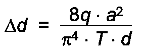
- The force exerted on the membrane when a voltage U is applied leads to a maximum deflection (q = electrostatic force in the plate capacitor)

where e is the distance between the capacitor plates. - e = 5 µm
U = ± 100 V
a = 2 mm ⇒ Δd = 2.6 µm
T = 10 N/mm²
d = 2 µm - For pneumatically deflecting the membrane by about 1.3 µm a pressure of about 80 Pa would be necessary.
- e = 20 µm
a = 10 mm ⇒ Δd = 8 µm
d = 1 µm
otherwise identical - o Neglecting the plate stiffness (i. e. only the tensile stress of the membrane is considered: this holds for thinner membranes).
- o d ≈ const.
- The calculations were based on maximum voltages of about 200 V. The electrode spacing was 5 µm and 20 µm, respectively. If the STM is used at normal air pressure, it has to be determined whether a voltage breakdown is taking place. The breakdown strength in a conventional electric actuator with an air gap is limited to approximately 3 X 10⁶ V/m by the electrical breakdown of air. For 200 V and a 10 µm gap, a breakdown strength of 2 X 10⁷ V/m is already obtained.
- The value of 3 X 10⁶ V/m no longer applies but begins to increase as the gap separation approaches a critical value. In this conjunction, see S. F. Bart et al. in Sensors and Actuators, 14 (1988) pp 269 - 292. For a gap of 12.5 µm, the value given is 3.2 X 10⁷ V/m. Other values in this article proceed from a maximum of 3 X 10⁸ V/m (p 273). These higher values indicate that an STM in accordance with the invention is feasible.
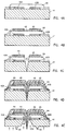
- Referring to Figs. 3A to 3G there is shown a first process comprising several steps for making an integrated scanning tunneling microscope using pneumatic and electrostatic control of tip motion in Z-direction and electrostatic control of X- and Y-scan of the tip. Fabrication starts with a substrate (31, Fig. 3A). Preferably this substrate is silicon or some other substrate suitable for forming integrated electronic circuits. The first step in the fabrication sequence is to deposit silicon dioxide layers (32) on either side of the substrate (31). Silicon nitride layers can also be used. Next, a pit of several µm depth is wet- or dry-etched into the front silicon dioxide layer (32) and into substrate (31) using for example buffered hydrofluoric acid for silicon dioxide and 37.5 % b. w. aqueous KOH for a silicon substrate. The size corresponds to the future membrane size (say, 2mm side length). The remaining silicon dioxide layer on the front side is then removed. The flat fine-etched pit is covered with a resistent mask (33, Fig. 3B). For example, silicon dioxide or aluminum can be used as mask materials. An opening is provided in masking layer (33) in the center of the pit, followed by etching a hole through the substrate (31, Fig. 3C). This etching step may be a dry-etching step using chlorine or bromine chemistry. The mask (33) is removed, and the front side including the deep hole is covered with a tensile stressed film (34). The film material which preferably is silicon carbide or silicon nitride is deposited by plasma enhanced chemical vapor deposition. The film thickness is, for example, 2 µm. The hole may have a diameter which is noticeably above 2 µm, depending upon the etch process, so that only the sidewalls and the bottom of the hole are covered with the film material. As a result, the future tip will be hollow, which seems appropriate for weight reasons (Fig. 3D).
- Next, the silicon dioxide mask (32) on the back side is opened, and the substrate (31) is thinned up by etching to the membrane (34) through the window thus obtained. A metallic electrode (36), consisting of Au or Al, is vapor-deposited on the front side of the membrane (34, Fig. 3E) using a molybdenum aperture mask. Two pairs of metallic electrodes X₁, X₂, Y₁ and Y₂ (37, 38) are formed on glass block (40) by vapor deposition of Au or Al (Fig. 3F) using a molybdenum aperture mask. The dimensions of glass block (40) may be, for example, 3x3x2 mm. As previously mentioned glass block (40) is provided with bores (43) which allow a pneumatical coarse approach of tip (35) in Z direction. Next, glass block (40) is bonded to the silicon frame (31, 34) with X, Y electrodes (37, 38) being positioned above Z electrode (36) on membrane (34) and membrane (34) with Z electrode being arranged on a lower plane. Bonding is "mallory" bonding effected at about 300 °C and 1000 V. Proof of the bonding between glass block and substrate could be established by means of the SiC intermediate layer (Fig. 3G).
- As up to this stage the tip (35) does not protrude from its surrounding silicon frame (31), the remaining silicon dioxide mask (32) on the back side is removed and the frame is thinned by etching. As the membrane material is an insulator, the tip (35) and a part of the membrane (34) and of silicon frame (31) on the bottom side have to be provided with an electrically conductive layer (39, Fig. 3G) to obtain voltage for the tunnel current. A preferred material for this layer is platinum which is applied with a thickness of about 0.1 µm.
- The deep hole (Fig. 3C) whose imprint forms the future tip (35) may be produced to have a diameter of 20 to 100 µm. In the event that problems occur during scanning as a result of this membrane hole, the hole would have to be closed in part or in full by the following additional steps. Following the silicon carbide or silicon nitride deposition step (34, Fig. 3D), the hole is filled with a polymeric material, preferably with polyimide, and planarized. After a baking step at about 400 °C, a second silicon carbide or silicon nitride layer is applied (not shown). This second silicon carbide or silicon nitride layer over the filled hole is partially opened in a reactive ion etching step, using a suitable mask such as a molybdenum mask with a lattice structure. In an oxygen plasma etching step, the polyimide is removed from the tip for weight reasons. This step yields a lattice spanning the hole, which does not allow a release of the membrane tension during scanning later on. It is assumed however that given a reasonably small hole with a diameter < 50 µm, such a supporting structure will not be required.
- Referring to Figs. 4A to 4E there is shown a second process comprising a planar technology for making an integrated scanning tunneling microscope.
- A layer of a conductive material, for example a 0.1 µm platinum layer, is applied to a substrate (41) by vapor deposition using a molybdenum aperture mask thereby obtaining four quadrants (42A, 42B, Fig. 4A) which are later on used as the lower electrodes for the X, Y and Z motion of the tip. The substrate is silicon or some other substrate material suitable for forming integrated electronic circuits. A silicon dioxide layer (44) is applied to the surface of the electrodes (42A, 42B) overlapping said electrodes for example by plasma enhanced chemical vapor deposition. This silicon dioxide layer with a thickness in the range of about 2 to 5 µm serves as a spacer layer between the lower and upper electrodes and will be removed later on by selective etching to space the electrodes.
- Next, an annular metal conductor (45), for example a 0.1 µm platinum conductor, is applied to silicon dioxide layer (44) by vapor deposition using a molybdenum aperture mask. This annular metal conductor which covers approximately the same area as the lower electrodes (42A, 42B) forms the common counter-electrode for the four quadrant electrodes. A dielectric layer (46), say of silicon carbide or silicon nitride, is deposited on top of said annular metal conductor (45, Fig. 4B) for example by plasma enhanced chemical vapor deposition. This material will not be attacked during the etching of silicon dioxide layer (44) with buffered hydrofluoric acid.
- A hole is provided in the center of the circular sandwich by reactive ion etching, followed by reactive ion etching of a tapered hole (47) through the silicon substrate (41), or of an inverted pyramid by anisotropic wet etching with for example 37.5 % b. w. aqueous KOH. This hole which extends nearly through the entire silicon wafer (41) forms a negative of the future tip which will be filled with the tunnel contact material and which is separated from the lower electrodes.
- The sandwich including the deep hole is covered with the tunnel contact material (48), for example with a 0.1 µm platinum layer, which deposited by vapor deposition using a molybdenum aperture mask. The tunnel current is fed through the conductor thus formed from the tip to the sample. To this conductor and to the entire structure a dielectric layer (49) of silicon carbide or silicon nitride is applied, using for example plasma enhanced chemical vapor deposition. The thickness of this layer may be 2 µm. This layer represents the oscillating membrane (49) to which the upper electrode (45) is connected by dielectric layer (46) and conductor (48, Fig. 4D).
- From the bottom side and by means of a structered oxide mask (not shown) the silicon surrounding the tip is removed, for example by etching with an aqueous solution of 37.5 % b. w. KOH. Subsequently, the whole wafer is slightly thinned around the 3 studs (50) using the same solution. By means of these studs the scanning tunneling microscope is positioned on the substrate to be investigated. The silicon dioxide layer (44) between the electrodes (42A, 42B and 45) is completely removed by etching with buffered hydrofluoric acid. This provides a clearance space for the membrane for moving along the H, Y and Z axes when electric fields are applied to the electrodes. The platinum-silicon carbide tip is connected to the membrane and can freely be moved by the same.
- On top of the scanning tunneling microscope described with reference to Figs. 4A to 4E a glass block may be arranged to allow pneumatical coarse approach of the membrane/tip assembly along Z-axis (not shown). A cavity is provided between the membrane (49) and the glass block to allow oscillation of the membrane. The glass block may be perforated for varying the damping of the membrane by subjecting the membrane to pressure, or, the cavity between the glass block and the membrane may be evacuated before bonding, with the bonding being used to obtain a vacuum-tight sealing.
- Advantages of the scanning tunneling microscope according to this invention are the hysteresis-free X-Y-Z drive and the high mechanical and thermal stability of the sensor head resulting from its low mass and small dimensions. As a result the arrangement is little susceptible to external vibrations. Control circuitry for the current supply for the distance control of the tip is integrated on the same semiconductor substrate. Furthermore, the signals resulting from scanning may be processed in the immediate vicinity of the sensor by circuits integrated on the same substrate.
Claims (19)
- Scanning tunneling microscope comprising at least one electron-emitting tip maintained at a relatively constant distance along a Z-axis normal to the sample surface, an XY-drive for scanning said tip in a matrix fashion across said sample surface, means for controlling a tunnel current between said tip and said sample surface to maintain said distance essentially constant,
characterized in that said XY-drive is an electrostatic transducer (10) and consists of at least four electrodes (27, 28; 37, 38; 42A, 42B) spaced from a counter-electrode (26, 36, 45);
said four electrodes (27, 28; 37, 38; 42A, 42B) being upper electrodes arranged on a member (40), or lower electrodes arranged on a substrate (41),
wherein said member (30, 40) is a perforated glass block which forms part of a pressure or vacuum generating chamber. - Scanning tunneling microscope of claim 1,
characterized in that said STM is fabricated by micromachining using integrated circuit processing steps. - Scanning tunneling microscope of claim 2,
characterized in that said STM is fabricated by a planar batch technique. - Scanning tunneling microscope of claims 1 to 3,
characterized in that said membrane (24, 34, 49) consists of a dielectric material, and that said tip (25, 35, 49) forming an integral part of said membrane is provided with an electrically conductive material (29, 39, 48) and connected to individual electrodes to which voltage may be applied for moving said tip along Z-axis normal to the sample surface. - Scanning tunneling microscope of claim 4,
characterized in that said membrane (24, 34, 49) consists of silicon carbide or silicon nitride, and said electrically conductive material (29,39,48) is platinum. - Scanning tunneling microscope of claims 1 to 5,
characterized in that for coarse approach of said membrane and integral tip along Z-axis the pressure on said membrane is varied, and that for fine approach of said membrane and integral tip a voltage Uz is applied to Z-electrode (26, 36, 45), the distance between tip and sample being controlled as a function of Uz. - Scanning tunneling microscope of one or several of claims 1 to 6,
characterized in that said membrane (24, 34, 49) is fixed to said glass block by a semiconductor substrate (21, 31, 41), wherein said semiconductor substrate (21, 31, 41) includes electronic devices for the current supply of the distance control of said tip and for processing the signals resulting from scanning. - Method of making a scanning tunneling microscope using pneumatic and electrostatic control of tip motion as claimed in claims 1 to 7, comprising the following steps:a) depositing masking layers (32) on either side of a semiconductor substrate (31); etching a pit of several µm depth into the front side masking layer (32) and into said substrate (31) in a size which corresponds to the future membrane size;b) removing said front side masking layer (32); depositing a resistant masking layer (33) on said etched pit;c) providing an opening in said resistant masking layer (33) in the center of said pit; etching a hole (35) through said substrate (31);d) removing the remaining masking layer (33); and covering the front side of said substrate (31) including said hole (35) with a tensile stressed film (34);e) opening said back side masking layer (32); thinning down said substrate (31) to expose said future membrane (34) and said tip (35); applying a metal layer (36) to said tensile stressed film (34) on the front side and patterning a first electrode so as to extend over said pit;f) applying a metal layer to a member (40) and patterning second electrodes (37, 38);g) bonding said member (40) with said second electrodes (37, 38) to the substrate frame (31, 34) with said second electrodes (37, 38) being positioned above said first electrode (36) on said membrane (34); and removing said remaining mask (32) from the back side of said substrate (31); thinning said substrate frame (31) by etching; and applying a metal coating (39) on said tip (35) and on a part of said substrate (31).
- Method of claim 8, wherein step a) of depositing said masking layer (32) comprises forming layers of silicon dioxide or silicon nitride on either side of said silicon substrate (31):
- Method of claim 8, wherein step b) of depositing a resistant mask material (33) comprises depositing silicon dioxide or aluminum.
- Method of claim 8, wherein step d) of covering the front side of said substrate (31) including said hole (35) with said tensile stressed film (34) comprises depositing silicon carbide or silicon nitride by plasma enhanced chemical vapor deposition.
- Method of claim 8 wherein the etching steps of said masking layers comprise wet-etching steps using buffered hydrofluoric acid for silicon dioxide.
- Method of claim 8 wherein the etching steps of said silicon substrate comprise wet-etching using a 37.5% b. w. aqueous KOH (steps a, e, g) or dry-etching using chlorine or bromine chemistry (step c).
- Method of claim 8, wherein depositing and patterning on said first and second electrodes comprise vapor depositing a metal, preferably platinum, using an aperture mask (steps e, f).
- Method of making a scanning tunneling microscope using pneumatic and electrostatic control of tip motion as claimed in claims 1 to 7, comprising the following steps:a) applying a first metal layer to a substrate (41) and patterning first electrodes (42A, 42B); and applying a first dielectric layer (44) to the surface of said first electrodes (42A, 42B) overlapping said electrodes;b) applying a second metal layer to said first dielectric layer (44) and patterning said metal layer to form an annular conductor (45) which covers approximately the same area as said first electrodes (42A, 42B) and which forms a second electrode; depositing a second dielectric layer (46) on top of said annular conductor (45);c) providing an opening in the center of said circular sandwich formed in step b) and etching a hole (47) through said substrate (41);d) covering said circular sandwich including said hole with tunnel contact material (48); applying a third dielectric layer (49) to said tunnel contact material layer (48) and to the entire structure;e) removing the substrate material surrounding the tip formed by said tunnel contact material (48) and by said third dielectric layer (49) in said hole (47) by etching using a structured oxide mask; thinning said substrate by etching; and etching off said first dielectric layer (44) so as to provide clearance space for said circular sandwich, comprising a membrane (49), said tunnel contact layer (48) with said tip (47) as integral part of said tunnel contact material and third dielectric layers (49, 48), said second dielectric layer (46), and said annular conductor (45), for moving along X, Y, and Z-axes upon application of electrical fields.
- Method of claim 15, wherein step a) of depositing a first dielectric layer (44) comprises depositing silicon dioxide which acts as a spacer material and which is removed by etching with buffered hydrofluoric acid at a later stage.
- Method of claim 15, wherein steps a, b, and d of depositing and patterning of said first electrodes (42A, 42B), of said annular conductor (45), and of said tunnel contact material (48) comprise vapor depositing a metal, preferably platinum, using an aperture mask.
- Method of claim 15, wherein steps b and d of depositing said first and third dielectric layers (44) and (49) comprise depositing silicon carbide or silicon nitride by plasma enhanced chemical vapor deposition, with said third dielectric layer (49) representing the membrane.
- Method of claims 15 to 18 further comprising: providing a glass block on top of said scanning tunneling microscope, leaving a cavity between said glass block and said membrane (49), to allow pneumatic coarse approach of the membrane/tip assembly along Z-axis normal to the sample surface.
Priority Applications (4)
| Application Number | Priority Date | Filing Date | Title |
|---|---|---|---|
| DE69023347T DE69023347T2 (en) | 1990-12-21 | 1990-12-21 | Integrated scanning tunneling microscope with pneumatic and electrostatic control and method for producing the same. |
| EP90125214A EP0491973B1 (en) | 1990-12-21 | 1990-12-21 | Integrated pneumatically and electrostatically controlled scanning tunneling microscope and method of making the same |
| JP3311345A JP2819518B2 (en) | 1990-12-21 | 1991-10-31 | Scanning tunnel microscope and manufacturing method thereof |
| US08/020,008 US5283437A (en) | 1990-12-21 | 1993-02-17 | Pneumatically and electrostatically driven scanning tunneling microscope |
Applications Claiming Priority (1)
| Application Number | Priority Date | Filing Date | Title |
|---|---|---|---|
| EP90125214A EP0491973B1 (en) | 1990-12-21 | 1990-12-21 | Integrated pneumatically and electrostatically controlled scanning tunneling microscope and method of making the same |
Publications (2)
| Publication Number | Publication Date |
|---|---|
| EP0491973A1 EP0491973A1 (en) | 1992-07-01 |
| EP0491973B1 true EP0491973B1 (en) | 1995-11-02 |
Family
ID=8204882
Family Applications (1)
| Application Number | Title | Priority Date | Filing Date |
|---|---|---|---|
| EP90125214A Expired - Lifetime EP0491973B1 (en) | 1990-12-21 | 1990-12-21 | Integrated pneumatically and electrostatically controlled scanning tunneling microscope and method of making the same |
Country Status (3)
| Country | Link |
|---|---|
| EP (1) | EP0491973B1 (en) |
| JP (1) | JP2819518B2 (en) |
| DE (1) | DE69023347T2 (en) |
Families Citing this family (8)
| Publication number | Priority date | Publication date | Assignee | Title |
|---|---|---|---|---|
| JP3184619B2 (en) * | 1991-09-24 | 2001-07-09 | キヤノン株式会社 | Parallel plane holding mechanism and memory device and STM device using the same |
| JP3402661B2 (en) * | 1992-07-06 | 2003-05-06 | キヤノン株式会社 | Cantilever probe and information processing apparatus using the same |
| US5553486A (en) * | 1993-10-01 | 1996-09-10 | Hysitron Incorporated | Apparatus for microindentation hardness testing and surface imaging incorporating a multi-plate capacitor system |
| US5658698A (en) * | 1994-01-31 | 1997-08-19 | Canon Kabushiki Kaisha | Microstructure, process for manufacturing thereof and devices incorporating the same |
| JP3192887B2 (en) * | 1994-09-21 | 2001-07-30 | キヤノン株式会社 | Probe, scanning probe microscope using the probe, and recording / reproducing apparatus using the probe |
| JP3182301B2 (en) * | 1994-11-07 | 2001-07-03 | キヤノン株式会社 | Microstructure and method for forming the same |
| JPH11304825A (en) * | 1997-09-30 | 1999-11-05 | Seiko Instruments Inc | Semiconductor distortion sensor and its manufacture, and scanning probe microscope |
| WO2010086759A1 (en) * | 2009-01-30 | 2010-08-05 | International Business Machines Corporation | High-speed scanning probe microscope |
Family Cites Families (5)
| Publication number | Priority date | Publication date | Assignee | Title |
|---|---|---|---|---|
| EP0194323B1 (en) * | 1985-03-07 | 1989-08-02 | International Business Machines Corporation | Scanning tunneling microscope |
| US4906840A (en) * | 1988-01-27 | 1990-03-06 | The Board Of Trustees Of Leland Stanford Jr., University | Integrated scanning tunneling microscope |
| DD298873A7 (en) * | 1988-11-07 | 1992-03-19 | Technische Universitaet Chemnitz,De | METHOD AND MEASURING HEAD FOR FINE CONTROL OF THE TUNNEL TIP OF A GRID TUNNEL MICROSCOPE |
| US4916002A (en) * | 1989-01-13 | 1990-04-10 | The Board Of Trustees Of The Leland Jr. University | Microcasting of microminiature tips |
| US5041783A (en) * | 1989-02-13 | 1991-08-20 | Olympus Optical Co., Ltd. | Probe unit for an atomic probe microscope |
-
1990
- 1990-12-21 DE DE69023347T patent/DE69023347T2/en not_active Expired - Lifetime
- 1990-12-21 EP EP90125214A patent/EP0491973B1/en not_active Expired - Lifetime
-
1991
- 1991-10-31 JP JP3311345A patent/JP2819518B2/en not_active Expired - Fee Related
Also Published As
| Publication number | Publication date |
|---|---|
| DE69023347D1 (en) | 1995-12-07 |
| EP0491973A1 (en) | 1992-07-01 |
| JPH04296604A (en) | 1992-10-21 |
| JP2819518B2 (en) | 1998-10-30 |
| DE69023347T2 (en) | 1996-05-30 |
Similar Documents
| Publication | Publication Date | Title |
|---|---|---|
| US5283437A (en) | Pneumatically and electrostatically driven scanning tunneling microscope | |
| US4912822A (en) | Method of making an integrated scanning tunneling microscope | |
| US5537863A (en) | Scanning probe microscope having a cantilever used therein | |
| US4916002A (en) | Microcasting of microminiature tips | |
| KR100748046B1 (en) | Apparatus for evaluating electrical characteristics | |
| US5166520A (en) | Universal, microfabricated probe for scanning probe microscopes | |
| Akamine et al. | A planar process for microfabrication of a scanning tunneling microscope | |
| EP0518618B1 (en) | Scanning tunneling microscope with cantilever type displacement element | |
| EP0786642A1 (en) | Method of manufacturing micro-tip for detecting tunneling current or micro-force or magnetic force, female mold substrate for manufacture thereof, method of manufacturing probe with micro-tip, probe unit, scanning probe microscope and information recording/reproduction apparatus having said probe | |
| JPH07333232A (en) | Formation of cantilever having probe | |
| EP0491973B1 (en) | Integrated pneumatically and electrostatically controlled scanning tunneling microscope and method of making the same | |
| US7161148B1 (en) | Tip structures, devices on their basis, and methods for their preparation | |
| Albrecht et al. | Microfabrication of integrated scanning tunneling microscope | |
| US6156216A (en) | Method for making nitride cantilevers devices | |
| Kim et al. | A 3-Dof MEMS motion stage for scanning tunneling microscopy | |
| JP2001108605A (en) | Cantilever for scanning-type probe microscope and its manufacturing method, and scaning-type probe microscope and surface charge-measuring microscope | |
| Kawai et al. | Resonator combined with a piezoelectric actuator for chemical analysis by force microscopy | |
| US11973441B2 (en) | MEMS nanopositioner and method of fabrication | |
| US20220368249A1 (en) | MEMS Nanopositioner and Method of Fabrication | |
| KR100388916B1 (en) | Cantilever for a scanning probe microscope and a method of manufacturing the same | |
| JPH0626807A (en) | Cantilever with thin-film type displacement sensor | |
| JPH06317404A (en) | Cantilever type actuator, scanning probe microscope using it, and information processor | |
| KR100486613B1 (en) | Elecron beam source module with carbon nano tube and method for fabricating the same | |
| JPH06241780A (en) | Scanning tunneling microscope, atomic force microscope, and machining device using them | |
| Chen et al. | From microgripping to nanogripping |
Legal Events
| Date | Code | Title | Description |
|---|---|---|---|
| PUAI | Public reference made under article 153(3) epc to a published international application that has entered the european phase |
Free format text: ORIGINAL CODE: 0009012 |
|
| 17P | Request for examination filed |
Effective date: 19901221 |
|
| AK | Designated contracting states |
Kind code of ref document: A1 Designated state(s): DE FR GB |
|
| 17Q | First examination report despatched |
Effective date: 19940812 |
|
| GRAA | (expected) grant |
Free format text: ORIGINAL CODE: 0009210 |
|
| AK | Designated contracting states |
Kind code of ref document: B1 Designated state(s): DE FR GB |
|
| PGFP | Annual fee paid to national office [announced via postgrant information from national office to epo] |
Ref country code: FR Payment date: 19951128 Year of fee payment: 6 |
|
| REF | Corresponds to: |
Ref document number: 69023347 Country of ref document: DE Date of ref document: 19951207 |
|
| ET | Fr: translation filed | ||
| PLBE | No opposition filed within time limit |
Free format text: ORIGINAL CODE: 0009261 |
|
| STAA | Information on the status of an ep patent application or granted ep patent |
Free format text: STATUS: NO OPPOSITION FILED WITHIN TIME LIMIT |
|
| 26N | No opposition filed | ||
| PG25 | Lapsed in a contracting state [announced via postgrant information from national office to epo] |
Ref country code: FR Effective date: 19970829 |
|
| REG | Reference to a national code |
Ref country code: FR Ref legal event code: ST |
|
| PGFP | Annual fee paid to national office [announced via postgrant information from national office to epo] |
Ref country code: GB Payment date: 19971119 Year of fee payment: 8 |
|
| PG25 | Lapsed in a contracting state [announced via postgrant information from national office to epo] |
Ref country code: GB Free format text: LAPSE BECAUSE OF NON-PAYMENT OF DUE FEES Effective date: 19981221 |
|
| GBPC | Gb: european patent ceased through non-payment of renewal fee |
Effective date: 19981221 |
|
| PGFP | Annual fee paid to national office [announced via postgrant information from national office to epo] |
Ref country code: DE Payment date: 20091221 Year of fee payment: 20 |
|
| PG25 | Lapsed in a contracting state [announced via postgrant information from national office to epo] |
Ref country code: DE Free format text: LAPSE BECAUSE OF EXPIRATION OF PROTECTION Effective date: 20101221 |