EP0488542A1 - Picture quality improving circuit - Google Patents
Picture quality improving circuit Download PDFInfo
- Publication number
- EP0488542A1 EP0488542A1 EP91310305A EP91310305A EP0488542A1 EP 0488542 A1 EP0488542 A1 EP 0488542A1 EP 91310305 A EP91310305 A EP 91310305A EP 91310305 A EP91310305 A EP 91310305A EP 0488542 A1 EP0488542 A1 EP 0488542A1
- Authority
- EP
- European Patent Office
- Prior art keywords
- circuit
- signal
- luminance signal
- input luminance
- cumulative histogram
- Prior art date
- Legal status (The legal status is an assumption and is not a legal conclusion. Google has not performed a legal analysis and makes no representation as to the accuracy of the status listed.)
- Granted
Links
- 230000001186 cumulative effect Effects 0.000 claims abstract description 54
- 238000005070 sampling Methods 0.000 claims description 6
- 238000010586 diagram Methods 0.000 description 8
- 238000010276 construction Methods 0.000 description 7
- 238000000034 method Methods 0.000 description 3
- 230000000694 effects Effects 0.000 description 1
- 230000010354 integration Effects 0.000 description 1
Images

Classifications
-
- G—PHYSICS
- G06—COMPUTING; CALCULATING OR COUNTING
- G06F—ELECTRIC DIGITAL DATA PROCESSING
- G06F17/00—Digital computing or data processing equipment or methods, specially adapted for specific functions
- G06F17/10—Complex mathematical operations
- G06F17/18—Complex mathematical operations for evaluating statistical data, e.g. average values, frequency distributions, probability functions, regression analysis
-
- G—PHYSICS
- G06—COMPUTING; CALCULATING OR COUNTING
- G06T—IMAGE DATA PROCESSING OR GENERATION, IN GENERAL
- G06T5/00—Image enhancement or restoration
- G06T5/40—Image enhancement or restoration by the use of histogram techniques
-
- G06T5/92—
-
- H—ELECTRICITY
- H04—ELECTRIC COMMUNICATION TECHNIQUE
- H04N—PICTORIAL COMMUNICATION, e.g. TELEVISION
- H04N5/00—Details of television systems
- H04N5/14—Picture signal circuitry for video frequency region
- H04N5/20—Circuitry for controlling amplitude response
Definitions
- This invention relates to picture quality improving technique for obtaining automatically an optimum image by catching the characteristics of an input image in apparatuses handling video signals such as a television receiver, a VCR, etc, particularly in apparatuses for digital processing signals in a video chromatic signal processing circuit.
- Digitization of apparatuses handling video signals has made steady progress in recent years and this trend has also spread to apparatuses for home and private use such as television receivers and VCRs. This technique is expected to reduce the number of necessary components and to improve reliability. Moreover, since a video chromatic signal processing circuit, in particular, can be easily developed to an EDTV due to digitization, this technique is believed to be very promising.
- CTR cathode-ray tube
- the dynamic range of the CRT is extremely narrower in comparison with natural light. This narrowness of the dynamic range in the display capacity imposes various limitations such as blooming which occurs in a scene where luminance signals are bright, and the problem that black gradation cannot be expressed in a dark scene.
- a cumulative histogram circuit defined in the appended Claim 1 comprises first to n th, or n , comparison circuits for inputting digital encoded input signals and comparing them with n, mutually different, reference values, respectively; and first to n th, or n , counters for inputting the output signals of the comparison circuits and carrying out a count-up operation when the reference values are greater, respectively; wherein the comparison operations are carried out up to a predetermined number of times to obtain a cumulative histogram at the output of each of the counters.
- the picture quality improving circuit defined in the appended Claim 2 comprises a first selector for inputting n signals, that is, the maximum value of an input luminance signal and first to (n - l)th cumulative histogram values, and selecting either one of the inputs by using upper m bits of the input luminance signals as a control signal; a second selector for inputting the signals of first to (n - l)th cumulative histogram values, and selecting either one of said inputs by using upper m bits of the input luminance signal as a control signal; a subtraction circuit for inputting the output signal of the first selector and the output signal of the second selector and calculating their difference; a multiplication circuit for inputting lower (l - m) bits of the input luminance signal and the output signal of the subtraction circuit, and multiplying them; and an addition circuit for adding the output signal of the multiplication circuit and the output signal of the second selector.
- the picture quality improving circuit defined in the appended Claim 3 comprises a cumulative histogram circuit for inputting a digital encoded input luminance signal and obtaining a cumulative histogram; a latch circuit for temporarily storing the histogram signal obtained by the cumulative histogram circuit; and an interpolation circuit for inputting the input luminance signal as well as the output histogram signal of the latch circuit and interpolating the input signal into a line graph similar to the histogram signal.
- an interpolation circuit which corrects a luminance signal in real time by the information of the cumulative histogram is provided.
- the cumulative histogram of the input luminance signal is directly calculated, which enables an operation in real time in the interpolation circuit on the basis of the result of calculation, and correction of picture quality by displaying the result of the operation.
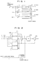
- Fig. 1 is a block diagram showing a cumulative histogram circuit claimed in the appended Claim 1. To simplify the description, this embodiment will be explained about the case where the distribution of a luminance signal is divided into four parts to obtain three histograms and interpolation is made between the four.
- reference numeral 11 denotes a first comparison circuit which receives a digital encoded 8-bit input luminance signal and compares this input luminance signal with a certain first reference value.
- Reference numeral 12 denotes a first counter which receives the output signal of the first comparison circuit 11 and makes a count-up operation when the first reference value (64) is greater.
- Reference numeral 13 denotes a second comparison circuit which receives the input luminance signal and compares the input luminance signal with a certain second reference value (128).
- Reference numeral 14 denotes a second counter which receives the output signal of the second comparison circuit 13 and makes a count-up operation when the second reference value is greater.
- Reference numeral 15 denotes a third comparison circuit which receives the input luminance signal and compares the input luminance signal with a certain third reference value (192).
- Reference numeral 16 denotes a third counter which receives the output signal of the third comparison circuit 15 and makes a count-up operation when the third reference value is greater.
- the input luminance signal is inputted to the three comparison circuits 11, 13 and 15, respectively.
- the first comparison circuit 11 outputs 0 because the input luminance signal is greater than the reference value (64) but the second and third comparison circuits 13 and 15 output 1 because the input luminance signal is smaller than the second and third reference values, respectively. Therefore, though the first counter 12 does not make its count-up operation, the second and third counters 14, 16 do make the count-up operation. If this sampling is effected 256 times, the output becomes automatically 256 because the value 256 is higher than all the input luminance signals, though the histogram when a luminance signal level is at 256 is not hereby taken. A cumulative histogram can be obtained by connecting 0, the output of the first counter 12, the output of the second counter 14, the output of the third counter 16 and 256.
- the picture quality improving circuit of this embodiment comprises the first comparison circuit which receives the digital encoded 8-bit input luminance signal and compares it with a certain reference value, the first counter which receives the output signal of the first comparison circuit and makes its count-up operation when the first reference value (64) is greater, a second comparison circuit which receives the input luminance signal and compares it with a certain second reference value (128), the second counter which receives the output signal of the second comparison circuit 13 and makes its count-up operation when the second reference value is greater, the third comparison circuit which receives the input luminance signal and compares it with a certain reference value (192), and the third counter which receives the output signal of the third comparison circuit 15 and makes its count-up operation when the third reference value is greater. Therefore, the cumulative histogram can be obtained at the output of each counter by effecting the comparison operaiton up to a predetermined number of times.
- Fig. 2 is a block diagram of an interpolation circuit claimed in the appended Claim 2.
- reference numeral 21 denotes a first selector which receives n signals from first and second cumulative histogram values to (n-l)th cumulative histogram value and selects any of the inputs by using upper m bits of the input luminance signal as a control signal.
- Reference numeral 22 denotes a second selector which receives the first, second to (n-l)th signals of the cumulative histogram values and selects any of the inputs by using the upper m bits of the input luminance signal as a control signal.
- Reference numeral 23 denotes a subtraction circuit which receives the output signal of the first selector 21 and that of the second selector 22 and calculates their difference.
- Reference numeral 24 denotes a multiplication circuit which receives the lower (n - m) bits of the input luminance signal as well as the output signal of the subtraction circuit described above, and carries out multiplication between them.
- Reference numeral 25 denotes an addition circuit which adds the output signal of the multiplication signal 24 to the output signal of the second selector 22.
- the abscissa represents the input luminance signal and the ordinate does the amplitude of the output signal of the interpolation circuit.
- dotted line represents the original characteristics and solid line does the interpolation characteristics which need to be obtained.
- the input luminance signal is 100
- its output value y can be obtained by the following equation (1) using the values m (64) and m (128) before and after the input luminance signal value 100 among the calculation results of histograms:
- (128 - 64) of the denominator is always 64 and constant in other regions, too. Since the region of distribution is divided into four parts in this embodiment, the denominator can be replaced by 64. This can be achieved by a hardware construction so as to shift 6 bits to lower bits.
- the upper 2 bits of the input luminance signal are first taken out in order to detect in which of the following ranges the level of the input signal exists: (0 - 63, 64 - 127, 128 - 191, 192 - 255) For, since the region is divided into four parts, it is possible to know in which region the numeric value exists, by referring to the upper 2 bits.
- the first selector 21 selects m (128) and the second selector 22 does m (64).
- the subtraction circuit 23 carries out subtraction between the output signal of the first selector 21 and the output signal of the second selector 22, and executes m (128) - m (64) of the equation (1).
- the output of the subtraction circuit 23 is shifted by 6 bits to the lower bits and is inputted as one of the inputs of the multiplication circuit 24.
- the lower 6 bits of the input luminance signal are inputted as the other input of the multiplication circuit 24, and multiplication is carried out between them.
- this embodiment can obtain the interpolated output in real time by the use of the result of cumulative histograms.
- Fig. 3 is a block diagram showing a picture quality improving circuit claimed in the appended Claim 3.
- a cumulative histogram circuit receiving a digital encoded input luminance signal for obtaining a cumulative histogram is represented by reference numeral 31.
- a latch circuit for temporarily storing the histogram signal obtained by the cumulative histogram circuit 31 is represented by reference numeral 32.
- An interpolation circuit receiving the input luminance signal and the output histogram signal of the latch circuit 32 for interpolating the input signal into a line graph similar to the histogram signal is represented by reference numeral 33.
- the picture quality improving circuit having the construction described above operates in the following way.
- the input luminance signal is inputted to the cumulative histogram circuit 31 to obtain the cumulative histogram of the input luminance signal.
- the output signal of the cumulative histogram circuit 31 is inputted to the latch circuit 32, which keeps this value until the cumulative histogram circuit 31 executes the next operation and outputs its output signal.
- the input luminance signal is inputted to the interpolation circuit 33 and its value is corrected by the use of the cumulative histogram outputted by the latch circuit 32.
- This correction operation is carried out in real time by effecting interpolation by the use of the data of the cumulative histogram.
- the output signals of the cumulative histogram circuit 31 describes an upwardly projecting graph as depicted in Fig. 4.
- the characteristics of this cumulative histogram are inputted to the interpolation circuit 33 through the latch circuit 32, and the luminance signal inputted to the interpolation circuit 33 is corrected to the output signal which is interpolated by this straight line. Accordingly, if the input luminance signal contains a large number of dark signals, the dark portion is stretched in a bright direction and outputted.
- a picture quality improving circuit which expands the dynamic range of the luminance signal by the luminance distribution of the input luminance signal can be obtained by providing the cumulative histogram circuit receiving the digital encoded input luminance signal for obtaining the cumulative histogram, the latch circuit for temporarily storing the histogram signals obtained in the cumulative histogram circuit, and the interpolation circuit receiving the input luminance signal and the output histogram signal of the latch circuit for interpolating the input signal into the line graph similar to the input histogram signal.
- division is made into four parts for the ease of explanation, but cumulative histograms of a greater number of divisions may be acquired by increasing the number of divisions and conducting more delicate control.
- the input luminance signal is the luminance signal of 256 steps (8-bits), by way of example. Therefore, the cumulative histogram of one cycle is obtained by conducting 256 times the counting operation. However, the cumulative histogram may be obtained by effecting N times this operation and then dividing the resulting cumulative histograms by N. In such a case, a cumulative histogram having higher stability may be obtained due to the integration effect even if any fluctuation exists in the input luminance signal.
- the continuous input luminance signals are measured in the first embodiment, the data throughout the entire screen can be effectively used if sampling is carried out with suitable intervals so that 256 sampling points exist throughout the screen.
- the present invention provides the picture quality improving circuit for expanding the dynamic range of the luminance signal according to the luminance distribution of the input luminance signal, which comprises the cumulative histogram circuit receiving the digital encoded input luminance signal for obtaining the cumulative histogram, the latch circuit for temporarily storing the histogram signal obtained in the cumulative histogram circuit, and the interpolation circuit receiving the input luminance signal as well as the output histogram signal of the latch circuit for interpolating the input signal into the line graph similar to the histogram signal.
Abstract
Description
- This invention relates to picture quality improving technique for obtaining automatically an optimum image by catching the characteristics of an input image in apparatuses handling video signals such as a television receiver, a VCR, etc, particularly in apparatuses for digital processing signals in a video chromatic signal processing circuit.
- Digitization of apparatuses handling video signals has made steady progress in recent years and this trend has also spread to apparatuses for home and private use such as television receivers and VCRs. This technique is expected to reduce the number of necessary components and to improve reliability. Moreover, since a video chromatic signal processing circuit, in particular, can be easily developed to an EDTV due to digitization, this technique is believed to be very promising.
- In analog television, on the other hand, a remarkable progress has been made and a very clear image can be reproduced, as well.
- However, both analog television and digital television use a cathode-ray tube (CRT), which is the most ordinary display device at present. However, the dynamic range of the CRT is extremely narrower in comparison with natural light. This narrowness of the dynamic range in the display capacity imposes various limitations such as blooming which occurs in a scene where luminance signals are bright, and the problem that black gradation cannot be expressed in a dark scene.
- To solve the problems described above, a cumulative histogram circuit defined in the appended Claim 1 comprises first to nth, or n, comparison circuits for inputting digital encoded input signals and comparing them with n, mutually different, reference values, respectively; and first to nth, or n, counters for inputting the output signals of the comparison circuits and carrying out a count-up operation when the reference values are greater, respectively; wherein the comparison operations are carried out up to a predetermined number of times to obtain a cumulative histogram at the output of each of the counters.
- The picture quality improving circuit defined in the appended
Claim 2 comprises a first selector for inputting n signals, that is, the maximum value of an input luminance signal and first to (n - l)th cumulative histogram values, and selecting either one of the inputs by using upper m bits of the input luminance signals as a control signal; a second selector for inputting the signals of first to (n - l)th cumulative histogram values, and selecting either one of said inputs by using upper m bits of the input luminance signal as a control signal; a subtraction circuit for inputting the output signal of the first selector and the output signal of the second selector and calculating their difference; a multiplication circuit for inputting lower (l - m) bits of the input luminance signal and the output signal of the subtraction circuit, and multiplying them; and an addition circuit for adding the output signal of the multiplication circuit and the output signal of the second selector. - The picture quality improving circuit defined in the appended
Claim 3 comprises a cumulative histogram circuit for inputting a digital encoded input luminance signal and obtaining a cumulative histogram; a latch circuit for temporarily storing the histogram signal obtained by the cumulative histogram circuit; and an interpolation circuit for inputting the input luminance signal as well as the output histogram signal of the latch circuit and interpolating the input signal into a line graph similar to the histogram signal. - According to the construction of Claim 1, luminance components of an input luminance signal as a cumulative histogram can be detected.
- According to the construction of
Claim 2, an interpolation circuit which corrects a luminance signal in real time by the information of the cumulative histogram is provided. - According to the construction of
Claim 3, the cumulative histogram of the input luminance signal, is directly calculated, which enables an operation in real time in the interpolation circuit on the basis of the result of calculation, and correction of picture quality by displaying the result of the operation. -
- Fig. 1 is a block diagram of a cumulative histogram circuit according to a first embodiment of the present invention;
- Fig. 2 is a block diagram of an interpolation circuit according to a second embodiment of the present invention;
- Fig. 3 is a block diagram of a picture quality correction circuit according to a third embodiment of the present invention; and
- Fig. 4 is a characteristic diagram useful for explaining the input signal from the cumulative histogram circuit in Fig. 2.
- Hereinafter, a cumulative histogram circuit in an embodiment of the present invention will be explained with reference to the accompanying drawings. Fig. 1 is a block diagram showing a cumulative histogram circuit claimed in the appended Claim 1. To simplify the description, this embodiment will be explained about the case where the distribution of a luminance signal is divided into four parts to obtain three histograms and interpolation is made between the four.
- In Fig. 1, reference numeral 11 denotes a first comparison circuit which receives a digital encoded 8-bit input luminance signal and compares this input luminance signal with a certain first reference value.
Reference numeral 12 denotes a first counter which receives the output signal of the first comparison circuit 11 and makes a count-up operation when the first reference value (64) is greater.Reference numeral 13 denotes a second comparison circuit which receives the input luminance signal and compares the input luminance signal with a certain second reference value (128).Reference numeral 14 denotes a second counter which receives the output signal of thesecond comparison circuit 13 and makes a count-up operation when the second reference value is greater.Reference numeral 15 denotes a third comparison circuit which receives the input luminance signal and compares the input luminance signal with a certain third reference value (192).Reference numeral 16 denotes a third counter which receives the output signal of thethird comparison circuit 15 and makes a count-up operation when the third reference value is greater. - The operation of the cumulative histogram circuit having the construction described above will be explained with reference to Fig. 1.
- To begin with, the input luminance signal is inputted to the three
comparison circuits third comparison circuits first counter 12 does not make its count-up operation, the second andthird counters value 256 is higher than all the input luminance signals, though the histogram when a luminance signal level is at 256 is not hereby taken. A cumulative histogram can be obtained by connecting 0, the output of thefirst counter 12, the output of thesecond counter 14, the output of thethird counter - As described above, the picture quality improving circuit of this embodiment comprises the first comparison circuit which receives the digital encoded 8-bit input luminance signal and compares it with a certain reference value, the first counter which receives the output signal of the first comparison circuit and makes its count-up operation when the first reference value (64) is greater, a second comparison circuit which receives the input luminance signal and compares it with a certain second reference value (128), the second counter which receives the output signal of the
second comparison circuit 13 and makes its count-up operation when the second reference value is greater, the third comparison circuit which receives the input luminance signal and compares it with a certain reference value (192), and the third counter which receives the output signal of thethird comparison circuit 15 and makes its count-up operation when the third reference value is greater. Therefore, the cumulative histogram can be obtained at the output of each counter by effecting the comparison operaiton up to a predetermined number of times. - Next, the second embodiment of the present invention will be explained with reference to the drawings. Fig. 2 is a block diagram of an interpolation circuit claimed in the appended
Claim 2. - In Fig. 2,
reference numeral 21 denotes a first selector which receives n signals from first and second cumulative histogram values to (n-l)th cumulative histogram value and selects any of the inputs by using upper m bits of the input luminance signal as a control signal.Reference numeral 22 denotes a second selector which receives the first, second to (n-l)th signals of the cumulative histogram values and selects any of the inputs by using the upper m bits of the input luminance signal as a control signal.Reference numeral 23 denotes a subtraction circuit which receives the output signal of thefirst selector 21 and that of thesecond selector 22 and calculates their difference.Reference numeral 24 denotes a multiplication circuit which receives the lower (n - m) bits of the input luminance signal as well as the output signal of the subtraction circuit described above, and carries out multiplication between them.Reference numeral 25 denotes an addition circuit which adds the output signal of themultiplication signal 24 to the output signal of thesecond selector 22. - The operation of the interpolation circuit having the construction described above will be explained with reference to Figs. 2 and 4.
- First of all, the numeric value which needs to be interpolated will be explained with reference to Fig. 4.
- In Fig. 4, the abscissa represents the input luminance signal and the ordinate does the amplitude of the output signal of the interpolation circuit. In this diagram, dotted line represents the original characteristics and solid line does the interpolation characteristics which need to be obtained.
- Assuming that the input luminance signal is 100, its output value y can be obtained by the following equation (1) using the values m (64) and m (128) before and after the input luminance signal value 100 among the calculation results of histograms:

In the equation given above, (128 - 64) of the denominator is always 64 and constant in other regions, too. Since the region of distribution is divided into four parts in this embodiment, the denominator can be replaced by 64. This can be achieved by a hardware construction so as to shift 6 bits to lower bits. - Next, an example in which the equation described above is executed will be explained with reference to Fig. 2.
- In Fig. 2, the upper 2 bits of the input luminance signal are first taken out in order to detect in which of the following ranges the level of the input signal exists:
(0 - 63, 64 - 127, 128 - 191, 192 - 255)
For, since the region is divided into four parts, it is possible to know in which region the numeric value exists, by referring to the upper 2 bits. - If the input signal is 100, for example, the upper two bits in binary code becomes 0lb. The suffix "b" represents that the numeric value is expressed by the binary code. At this time, the
first selector 21 selects m (128) and thesecond selector 22 does m (64). Thesubtraction circuit 23 carries out subtraction between the output signal of thefirst selector 21 and the output signal of thesecond selector 22, and executes m (128) - m (64) of the equation (1). Next, the output of thesubtraction circuit 23 is shifted by 6 bits to the lower bits and is inputted as one of the inputs of themultiplication circuit 24. The lower 6 bits of the input luminance signal are inputted as the other input of themultiplication circuit 24, and multiplication is carried out between them. These operations accomplish the division by (128 - 64) and subtraction (100 - 64) in the first term of the equation (1). Next, the output signal of themultiplication circuit 24 is inputted as one of the inputs of theaddition circuit 25 and thevalue 64 is inputted as the other so as to carry out addition between them. In this way, the addition of the second term of the equation (2) is achieved. - As described above, this embodiment can obtain the interpolated output in real time by the use of the result of cumulative histograms.
- The third embodiment of the present invention will now be described with reference to the drawings. Fig. 3 is a block diagram showing a picture quality improving circuit claimed in the appended
Claim 3. - Referring to Fig. 3, a cumulative histogram circuit receiving a digital encoded input luminance signal for obtaining a cumulative histogram is represented by
reference numeral 31. A latch circuit for temporarily storing the histogram signal obtained by thecumulative histogram circuit 31 is represented byreference numeral 32. An interpolation circuit receiving the input luminance signal and the output histogram signal of thelatch circuit 32 for interpolating the input signal into a line graph similar to the histogram signal is represented byreference numeral 33. - The picture quality improving circuit having the construction described above operates in the following way.
- The input luminance signal is inputted to the
cumulative histogram circuit 31 to obtain the cumulative histogram of the input luminance signal. The output signal of thecumulative histogram circuit 31 is inputted to thelatch circuit 32, which keeps this value until thecumulative histogram circuit 31 executes the next operation and outputs its output signal. - On the other hand, the input luminance signal is inputted to the
interpolation circuit 33 and its value is corrected by the use of the cumulative histogram outputted by thelatch circuit 32. This correction operation is carried out in real time by effecting interpolation by the use of the data of the cumulative histogram. - If, for example, the luminance distribution of the input luminance signals has a large number of dark signals, the output signals of the
cumulative histogram circuit 31 describes an upwardly projecting graph as depicted in Fig. 4. The characteristics of this cumulative histogram are inputted to theinterpolation circuit 33 through thelatch circuit 32, and the luminance signal inputted to theinterpolation circuit 33 is corrected to the output signal which is interpolated by this straight line. Accordingly, if the input luminance signal contains a large number of dark signals, the dark portion is stretched in a bright direction and outputted. - As described above, a picture quality improving circuit which expands the dynamic range of the luminance signal by the luminance distribution of the input luminance signal can be obtained by providing the cumulative histogram circuit receiving the digital encoded input luminance signal for obtaining the cumulative histogram, the latch circuit for temporarily storing the histogram signals obtained in the cumulative histogram circuit, and the interpolation circuit receiving the input luminance signal and the output histogram signal of the latch circuit for interpolating the input signal into the line graph similar to the input histogram signal.
- In the first embodiment described above, division is made into four parts for the ease of explanation, but cumulative histograms of a greater number of divisions may be acquired by increasing the number of divisions and conducting more delicate control.
- In the first embodiment, the input luminance signal is the luminance signal of 256 steps (8-bits), by way of example. Therefore, the cumulative histogram of one cycle is obtained by conducting 256 times the counting operation. However, the cumulative histogram may be obtained by effecting N times this operation and then dividing the resulting cumulative histograms by N. In such a case, a cumulative histogram having higher stability may be obtained due to the integration effect even if any fluctuation exists in the input luminance signal.
- Though the continuous input luminance signals are measured in the first embodiment, the data throughout the entire screen can be effectively used if sampling is carried out with suitable intervals so that 256 sampling points exist throughout the screen.
- If the data of the full surface of the screen are used in the first embodiment as described above, an error is likely to occur. If a motion picture of a panorama size is vertically cut by black and is transmitted in a so-called "letter box", for example, a large number of black portions which are not the image portions and wrong cumulative histogram will be obtained if the data of the full surface of the screen are employed. In such a case, the operation should be carried out by the luminance signals only at the center portion of the screen and the upper and lower portions of the screen should be masked.
- As described above, the present invention provides the picture quality improving circuit for expanding the dynamic range of the luminance signal according to the luminance distribution of the input luminance signal, which comprises the cumulative histogram circuit receiving the digital encoded input luminance signal for obtaining the cumulative histogram, the latch circuit for temporarily storing the histogram signal obtained in the cumulative histogram circuit, and the interpolation circuit receiving the input luminance signal as well as the output histogram signal of the latch circuit for interpolating the input signal into the line graph similar to the histogram signal.
Claims (5)
- A picture quality improving circuit comprising:
first to nth, or n, comparison circuits (11, 13, 15) receiving digital encoded input signals for comparing them with n, mutually different, reference values, respectively; and
first to nth, or n, counters (12, 14, 16) receiving the output signals of said comparison circuits for carrying out a count-up operation when said reference values are greater, respectively;
wherein the comparison operations are carried out up to a predetermined number of times to obtain a cumulative histogram at the output of each of said counters. - A picture quality improving circuit comprising:
a first selector (21) receiving n signals, that is, the maximum value of an input luminance signal and first to (n - l)th cumulative histogram values, for selecting either one of said inputs by using upper m bits of said input luminance signal as a control signal;
a second selector (22) receiving the signals of first to (n - l)th cumulative histogram values, for selecting either one of said inputs by using upper m bits of said input luminance signal as a control signal;
a subtraction circuit (23) receiving the output signal of said first selector and the output signal of said second selector, for calculating their difference;
a multiplication circuit (24) receiving lower (l - m) bits of said input luminance signal and the output signal of said subtraction circuit, for multiplying them; and
an addition circuit (25) for adding the output signal of said multiplication circuit and the output signal of said second selector. - A picture quality improving circuit comprising:
a cumulative histogram circuit (31) receiving a digital encoded input luminance signal for obtaining a cumulative histogram;
a latch circuit (32) for temporarily storing said histogram signal obtained by said cumulative histogram circuit; and
an interpolation circuit (33) receiving said input luminance signal as well as the output histogram signal of said latch circuit for interpolating said input signal into a line graph similar to said histogram signal. - A picture quality improving circuit according to claim 1, wherein sampling is carried out in intervals such that 256 sampling points exist throughout the full surface of a screen.
- A picture quality improving circuit according to claim 1, wherein sampling is carried out in such a manner that an operation is carried out only at the center portion of the screen by said luminance signal and the upper and lower portions of the screen are masked.
Applications Claiming Priority (2)
| Application Number | Priority Date | Filing Date | Title |
|---|---|---|---|
| JP2313542A JPH04183177A (en) | 1990-11-19 | 1990-11-19 | Accumulating histogram circuit, interpolating circuit, and image quality compensating circuit |
| JP313542/90 | 1990-11-19 |
Publications (2)
| Publication Number | Publication Date |
|---|---|
| EP0488542A1 true EP0488542A1 (en) | 1992-06-03 |
| EP0488542B1 EP0488542B1 (en) | 1996-03-06 |
Family
ID=18042578
Family Applications (1)
| Application Number | Title | Priority Date | Filing Date |
|---|---|---|---|
| EP91310305A Expired - Lifetime EP0488542B1 (en) | 1990-11-19 | 1991-11-07 | Picture quality improving circuit |
Country Status (3)
| Country | Link |
|---|---|
| EP (1) | EP0488542B1 (en) |
| JP (1) | JPH04183177A (en) |
| DE (1) | DE69117677T2 (en) |
Cited By (10)
| Publication number | Priority date | Publication date | Assignee | Title |
|---|---|---|---|---|
| EP0548781A2 (en) * | 1991-12-20 | 1993-06-30 | Matsushita Electric Industrial Co., Ltd. | Gradation compensation apparatus of video image |
| EP0570873A2 (en) * | 1992-05-22 | 1993-11-24 | Thomson Consumer Electronics, Inc. | Non-linear video signal processor employing picture element analysis |
| EP0639915A1 (en) * | 1993-08-20 | 1995-02-22 | Hitachi, Ltd. | A technique for automatically detecting the constellation size of a quadrature amplitude modulated (QAM) signal |
| DE4430629A1 (en) * | 1993-09-03 | 1995-03-09 | Matsushita Electric Ind Co Ltd | Digital image processing device |
| EP0648043A1 (en) * | 1993-10-08 | 1995-04-12 | Koninklijke Philips Electronics N.V. | Picture signal enhancement circuit |
| EP0654942A1 (en) * | 1993-11-23 | 1995-05-24 | Koninklijke Philips Electronics N.V. | Non-linear signal processing |
| EP0801509A2 (en) * | 1996-04-12 | 1997-10-15 | Sony Corporation | Video camera, video signal processing, video signal compression and video signal conversion |
| EP0817120A2 (en) * | 1996-06-27 | 1998-01-07 | Samsung Electronics Co., Ltd. | Image histogram equalization circuit and method therefor |
| EP0860795A1 (en) * | 1997-02-21 | 1998-08-26 | Samsung Electronics Co., Ltd. | Method and circuit for extracting histogram and cumulative distribution function for image enhancement apparatus |
| WO1998039912A1 (en) * | 1997-03-06 | 1998-09-11 | Matsushita Electric Industrial Co., Ltd. | Histogram generator |
Families Citing this family (2)
| Publication number | Priority date | Publication date | Assignee | Title |
|---|---|---|---|---|
| US7139426B2 (en) * | 2002-02-12 | 2006-11-21 | Tektronix, Inc. | Histogram data collector for applying progressively adjusted histogram equalization to an oscilloscope image |
| JP4557090B2 (en) * | 2009-11-10 | 2010-10-06 | セイコーエプソン株式会社 | Image processing apparatus, image processing method, and image processing program |
Citations (4)
| Publication number | Priority date | Publication date | Assignee | Title |
|---|---|---|---|---|
| US3979555A (en) * | 1975-05-27 | 1976-09-07 | Hughes Aircraft Company | Histogram equalization system for display improvement |
| FR2452216A1 (en) * | 1979-03-21 | 1980-10-17 | Hajime Industries | Image analyser for inspection purposes - incorporates circuit with several light-dark reference levels, using closed circuit TV pick=up |
| EP0034737A1 (en) * | 1980-02-13 | 1981-09-02 | Siemens-Albis Aktiengesellschaft | Method for improving the definition of a video image |
| US4337514A (en) * | 1979-05-11 | 1982-06-29 | Thomson-Csf | Device for automatically controlling the transfer function of a video system for improving image perception |
Family Cites Families (3)
| Publication number | Priority date | Publication date | Assignee | Title |
|---|---|---|---|---|
| JPS6273867A (en) * | 1985-09-26 | 1987-04-04 | Canon Inc | Picture separating method |
| JPH0248728A (en) * | 1988-08-10 | 1990-02-19 | Toshiba Corp | Window processor |
| JPH02268082A (en) * | 1989-04-10 | 1990-11-01 | Fuji Xerox Co Ltd | Picture segmenting method |
-
1990
- 1990-11-19 JP JP2313542A patent/JPH04183177A/en active Pending
-
1991
- 1991-11-07 EP EP91310305A patent/EP0488542B1/en not_active Expired - Lifetime
- 1991-11-07 DE DE69117677T patent/DE69117677T2/en not_active Expired - Fee Related
Patent Citations (4)
| Publication number | Priority date | Publication date | Assignee | Title |
|---|---|---|---|---|
| US3979555A (en) * | 1975-05-27 | 1976-09-07 | Hughes Aircraft Company | Histogram equalization system for display improvement |
| FR2452216A1 (en) * | 1979-03-21 | 1980-10-17 | Hajime Industries | Image analyser for inspection purposes - incorporates circuit with several light-dark reference levels, using closed circuit TV pick=up |
| US4337514A (en) * | 1979-05-11 | 1982-06-29 | Thomson-Csf | Device for automatically controlling the transfer function of a video system for improving image perception |
| EP0034737A1 (en) * | 1980-02-13 | 1981-09-02 | Siemens-Albis Aktiengesellschaft | Method for improving the definition of a video image |
Cited By (25)
| Publication number | Priority date | Publication date | Assignee | Title |
|---|---|---|---|---|
| US5296941A (en) * | 1991-12-20 | 1994-03-22 | Matsushita Electric Industrial Co, Ltd. | Gradation compensation apparatus of video image |
| EP0548781A3 (en) * | 1991-12-20 | 1993-08-11 | Matsushita Electric Industrial Co., Ltd. | Gradation compensation apparatus of video image |
| EP0548781A2 (en) * | 1991-12-20 | 1993-06-30 | Matsushita Electric Industrial Co., Ltd. | Gradation compensation apparatus of video image |
| US5422680A (en) * | 1992-05-22 | 1995-06-06 | Thomson Consumer Electronics, Inc. | Non-linear contrast control apparatus with pixel distribution measurement for video display system |
| EP0570873A3 (en) * | 1992-05-22 | 1994-02-16 | Thomson Consumer Electronics | |
| EP0570873A2 (en) * | 1992-05-22 | 1993-11-24 | Thomson Consumer Electronics, Inc. | Non-linear video signal processor employing picture element analysis |
| CN1037223C (en) * | 1992-05-22 | 1998-01-28 | 汤姆森消费电子有限公司 | Non-linear video signal processor employing picture element analysis |
| EP0639915A1 (en) * | 1993-08-20 | 1995-02-22 | Hitachi, Ltd. | A technique for automatically detecting the constellation size of a quadrature amplitude modulated (QAM) signal |
| DE4430629A1 (en) * | 1993-09-03 | 1995-03-09 | Matsushita Electric Ind Co Ltd | Digital image processing device |
| US6442294B1 (en) | 1993-09-03 | 2002-08-27 | Matsushita Electric Industrial Co., Ltd. | Digital image processing apparatus with interpolation and adder circuits |
| EP0648043A1 (en) * | 1993-10-08 | 1995-04-12 | Koninklijke Philips Electronics N.V. | Picture signal enhancement circuit |
| US5734746A (en) * | 1993-10-08 | 1998-03-31 | U.S. Philips Corporation | Picture signal enhancement circuit includes a non-linear circuit for enhancing the picture signal in dependence of histograms measured at transitions in the picture signal |
| BE1007608A3 (en) * | 1993-10-08 | 1995-08-22 | Philips Electronics Nv | Improving picture signal circuit. |
| EP0654942A1 (en) * | 1993-11-23 | 1995-05-24 | Koninklijke Philips Electronics N.V. | Non-linear signal processing |
| BE1007777A3 (en) * | 1993-11-23 | 1995-10-17 | Philips Electronics Nv | Non-linear signal. |
| EP0801509A2 (en) * | 1996-04-12 | 1997-10-15 | Sony Corporation | Video camera, video signal processing, video signal compression and video signal conversion |
| EP0801509A3 (en) * | 1996-04-12 | 2000-08-30 | Sony Corporation | Video camera, video signal processing, video signal compression and video signal conversion |
| EP0817120A3 (en) * | 1996-06-27 | 1998-11-11 | Samsung Electronics Co., Ltd. | Image histogram equalization circuit and method therefor |
| US6075890A (en) * | 1996-06-27 | 2000-06-13 | Samsung Electronics Co., Ltd. | Video-image histogram equalization circuit and method therefor |
| EP0817120A2 (en) * | 1996-06-27 | 1998-01-07 | Samsung Electronics Co., Ltd. | Image histogram equalization circuit and method therefor |
| EP0860795A1 (en) * | 1997-02-21 | 1998-08-26 | Samsung Electronics Co., Ltd. | Method and circuit for extracting histogram and cumulative distribution function for image enhancement apparatus |
| CN1094623C (en) * | 1997-02-21 | 2002-11-20 | 三星电子株式会社 | Method and circuit for extracting histogram and cumulative distribution function for image enhancement apparatus |
| WO1998039912A1 (en) * | 1997-03-06 | 1998-09-11 | Matsushita Electric Industrial Co., Ltd. | Histogram generator |
| US6252983B1 (en) | 1997-03-06 | 2001-06-26 | Matsushita Electric Industrial Co., Ltd. | Histogram generator |
| CN1120615C (en) * | 1997-03-06 | 2003-09-03 | 松下电器产业株式会社 | Histogram generator |
Also Published As
| Publication number | Publication date |
|---|---|
| JPH04183177A (en) | 1992-06-30 |
| EP0488542B1 (en) | 1996-03-06 |
| DE69117677D1 (en) | 1996-04-11 |
| DE69117677T2 (en) | 1996-10-31 |
Similar Documents
| Publication | Publication Date | Title |
|---|---|---|
| US5388168A (en) | Picture quality improving circuit using a cumulative histogram | |
| KR100207660B1 (en) | Picture quality improving method and circuit using quantized histogram equalization | |
| US6259472B1 (en) | Histogram equalization apparatus for contrast enhancement of moving image and method therefor | |
| US6894666B2 (en) | Contrast correcting circuit | |
| US5748231A (en) | Adaptive motion vector decision method and device for digital image stabilizer system | |
| JP3962876B2 (en) | Interpolation filter for video signal | |
| EP0348207A2 (en) | Image motion vector detecting apparatus | |
| US20040001165A1 (en) | Image processing apparatus and image processing method | |
| US6456660B1 (en) | Device and method of detecting motion vectors | |
| US5357287A (en) | Method of and apparatus for motion estimation of video data | |
| EP0488542A1 (en) | Picture quality improving circuit | |
| US6614485B2 (en) | Deinterlacing apparatus | |
| EP0551189A2 (en) | Video signal correction system | |
| EP1104970B1 (en) | Method and device for converting number of frames of image signals | |
| US6442294B1 (en) | Digital image processing apparatus with interpolation and adder circuits | |
| KR20000073265A (en) | apparatus and method for controlling brightness in image signal | |
| US20030059126A1 (en) | Apparatus and method for line interpolating of image signal | |
| KR100397904B1 (en) | GRADATION CORRECTION CIRCUIT, AND γCORRECTION APPARATUS | |
| EP0554836A2 (en) | Parabolic waveform generating apparatus | |
| JP3255258B2 (en) | Image display device | |
| US4217574A (en) | Analog to digital converter having nonlinear amplitude transformation | |
| US5508751A (en) | Recursive noise reduction device for reducing noise of stationary regions in moving images | |
| JPH1098695A (en) | Image information converter and its device and product sum arithmetic unit | |
| US7042524B2 (en) | Video data correction device and video data correction method | |
| US5719793A (en) | Recursive noise reduction device having improved adaptability with respect to input image data |
Legal Events
| Date | Code | Title | Description |
|---|---|---|---|
| PUAI | Public reference made under article 153(3) epc to a published international application that has entered the european phase |
Free format text: ORIGINAL CODE: 0009012 |
|
| AK | Designated contracting states |
Kind code of ref document: A1 Designated state(s): DE FR GB IT |
|
| 17P | Request for examination filed |
Effective date: 19920708 |
|
| 17Q | First examination report despatched |
Effective date: 19940517 |
|
| ITF | It: translation for a ep patent filed |
Owner name: BARZANO' E ZANARDO ROMA S.P.A. |
|
| GRAA | (expected) grant |
Free format text: ORIGINAL CODE: 0009210 |
|
| AK | Designated contracting states |
Kind code of ref document: B1 Designated state(s): DE FR GB IT |
|
| REF | Corresponds to: |
Ref document number: 69117677 Country of ref document: DE Date of ref document: 19960411 |
|
| ET | Fr: translation filed | ||
| PLBE | No opposition filed within time limit |
Free format text: ORIGINAL CODE: 0009261 |
|
| STAA | Information on the status of an ep patent application or granted ep patent |
Free format text: STATUS: NO OPPOSITION FILED WITHIN TIME LIMIT |
|
| 26N | No opposition filed | ||
| PGFP | Annual fee paid to national office [announced via postgrant information from national office to epo] |
Ref country code: GB Payment date: 20011107 Year of fee payment: 11 |
|
| PGFP | Annual fee paid to national office [announced via postgrant information from national office to epo] |
Ref country code: FR Payment date: 20011113 Year of fee payment: 11 |
|
| PGFP | Annual fee paid to national office [announced via postgrant information from national office to epo] |
Ref country code: DE Payment date: 20011119 Year of fee payment: 11 |
|
| REG | Reference to a national code |
Ref country code: GB Ref legal event code: IF02 |
|
| PG25 | Lapsed in a contracting state [announced via postgrant information from national office to epo] |
Ref country code: GB Free format text: LAPSE BECAUSE OF NON-PAYMENT OF DUE FEES Effective date: 20021107 |
|
| PG25 | Lapsed in a contracting state [announced via postgrant information from national office to epo] |
Ref country code: DE Free format text: LAPSE BECAUSE OF NON-PAYMENT OF DUE FEES Effective date: 20030603 |
|
| GBPC | Gb: european patent ceased through non-payment of renewal fee | ||
| PG25 | Lapsed in a contracting state [announced via postgrant information from national office to epo] |
Ref country code: FR Free format text: LAPSE BECAUSE OF NON-PAYMENT OF DUE FEES Effective date: 20030731 |
|
| REG | Reference to a national code |
Ref country code: FR Ref legal event code: ST |
|
| PG25 | Lapsed in a contracting state [announced via postgrant information from national office to epo] |
Ref country code: IT Free format text: LAPSE BECAUSE OF NON-PAYMENT OF DUE FEES;WARNING: LAPSES OF ITALIAN PATENTS WITH EFFECTIVE DATE BEFORE 2007 MAY HAVE OCCURRED AT ANY TIME BEFORE 2007. THE CORRECT EFFECTIVE DATE MAY BE DIFFERENT FROM THE ONE RECORDED. Effective date: 20051107 |