EP0488230A2 - Method of manufacturing a semiconductor substrate having a dielectric isolation structure - Google Patents
Method of manufacturing a semiconductor substrate having a dielectric isolation structure Download PDFInfo
- Publication number
- EP0488230A2 EP0488230A2 EP91120294A EP91120294A EP0488230A2 EP 0488230 A2 EP0488230 A2 EP 0488230A2 EP 91120294 A EP91120294 A EP 91120294A EP 91120294 A EP91120294 A EP 91120294A EP 0488230 A2 EP0488230 A2 EP 0488230A2
- Authority
- EP
- European Patent Office
- Prior art keywords
- layer
- semiconductor
- type silicon
- silicon layer
- semiconductor substrate
- Prior art date
- Legal status (The legal status is an assumption and is not a legal conclusion. Google has not performed a legal analysis and makes no representation as to the accuracy of the status listed.)
- Granted
Links
Images


Classifications
-
- H—ELECTRICITY
- H01—ELECTRIC ELEMENTS
- H01L—SEMICONDUCTOR DEVICES NOT COVERED BY CLASS H10
- H01L21/00—Processes or apparatus adapted for the manufacture or treatment of semiconductor or solid state devices or of parts thereof
- H01L21/02—Manufacture or treatment of semiconductor devices or of parts thereof
- H01L21/04—Manufacture or treatment of semiconductor devices or of parts thereof the devices having at least one potential-jump barrier or surface barrier, e.g. PN junction, depletion layer or carrier concentration layer
- H01L21/18—Manufacture or treatment of semiconductor devices or of parts thereof the devices having at least one potential-jump barrier or surface barrier, e.g. PN junction, depletion layer or carrier concentration layer the devices having semiconductor bodies comprising elements of Group IV of the Periodic System or AIIIBV compounds with or without impurities, e.g. doping materials
- H01L21/30—Treatment of semiconductor bodies using processes or apparatus not provided for in groups H01L21/20 - H01L21/26
- H01L21/31—Treatment of semiconductor bodies using processes or apparatus not provided for in groups H01L21/20 - H01L21/26 to form insulating layers thereon, e.g. for masking or by using photolithographic techniques; After treatment of these layers; Selection of materials for these layers
- H01L21/3205—Deposition of non-insulating-, e.g. conductive- or resistive-, layers on insulating layers; After-treatment of these layers
- H01L21/321—After treatment
- H01L21/32115—Planarisation
- H01L21/3212—Planarisation by chemical mechanical polishing [CMP]
-
- H—ELECTRICITY
- H01—ELECTRIC ELEMENTS
- H01L—SEMICONDUCTOR DEVICES NOT COVERED BY CLASS H10
- H01L21/00—Processes or apparatus adapted for the manufacture or treatment of semiconductor or solid state devices or of parts thereof
- H01L21/70—Manufacture or treatment of devices consisting of a plurality of solid state components formed in or on a common substrate or of parts thereof; Manufacture of integrated circuit devices or of parts thereof
- H01L21/71—Manufacture of specific parts of devices defined in group H01L21/70
- H01L21/76—Making of isolation regions between components
- H01L21/762—Dielectric regions, e.g. EPIC dielectric isolation, LOCOS; Trench refilling techniques, SOI technology, use of channel stoppers
- H01L21/7624—Dielectric regions, e.g. EPIC dielectric isolation, LOCOS; Trench refilling techniques, SOI technology, use of channel stoppers using semiconductor on insulator [SOI] technology
- H01L21/76264—SOI together with lateral isolation, e.g. using local oxidation of silicon, or dielectric or polycristalline material refilled trench or air gap isolation regions, e.g. completely isolated semiconductor islands
-
- H—ELECTRICITY
- H01—ELECTRIC ELEMENTS
- H01L—SEMICONDUCTOR DEVICES NOT COVERED BY CLASS H10
- H01L21/00—Processes or apparatus adapted for the manufacture or treatment of semiconductor or solid state devices or of parts thereof
- H01L21/70—Manufacture or treatment of devices consisting of a plurality of solid state components formed in or on a common substrate or of parts thereof; Manufacture of integrated circuit devices or of parts thereof
- H01L21/71—Manufacture of specific parts of devices defined in group H01L21/70
- H01L21/76—Making of isolation regions between components
- H01L21/763—Polycrystalline semiconductor regions
-
- H—ELECTRICITY
- H01—ELECTRIC ELEMENTS
- H01L—SEMICONDUCTOR DEVICES NOT COVERED BY CLASS H10
- H01L21/00—Processes or apparatus adapted for the manufacture or treatment of semiconductor or solid state devices or of parts thereof
- H01L21/70—Manufacture or treatment of devices consisting of a plurality of solid state components formed in or on a common substrate or of parts thereof; Manufacture of integrated circuit devices or of parts thereof
- H01L21/71—Manufacture of specific parts of devices defined in group H01L21/70
- H01L21/76—Making of isolation regions between components
- H01L21/762—Dielectric regions, e.g. EPIC dielectric isolation, LOCOS; Trench refilling techniques, SOI technology, use of channel stoppers
- H01L21/7624—Dielectric regions, e.g. EPIC dielectric isolation, LOCOS; Trench refilling techniques, SOI technology, use of channel stoppers using semiconductor on insulator [SOI] technology
- H01L21/76264—SOI together with lateral isolation, e.g. using local oxidation of silicon, or dielectric or polycristalline material refilled trench or air gap isolation regions, e.g. completely isolated semiconductor islands
- H01L21/76275—Vertical isolation by bonding techniques
-
- H—ELECTRICITY
- H01—ELECTRIC ELEMENTS
- H01L—SEMICONDUCTOR DEVICES NOT COVERED BY CLASS H10
- H01L21/00—Processes or apparatus adapted for the manufacture or treatment of semiconductor or solid state devices or of parts thereof
- H01L21/70—Manufacture or treatment of devices consisting of a plurality of solid state components formed in or on a common substrate or of parts thereof; Manufacture of integrated circuit devices or of parts thereof
- H01L21/71—Manufacture of specific parts of devices defined in group H01L21/70
- H01L21/76—Making of isolation regions between components
- H01L21/762—Dielectric regions, e.g. EPIC dielectric isolation, LOCOS; Trench refilling techniques, SOI technology, use of channel stoppers
- H01L21/7624—Dielectric regions, e.g. EPIC dielectric isolation, LOCOS; Trench refilling techniques, SOI technology, use of channel stoppers using semiconductor on insulator [SOI] technology
- H01L21/76264—SOI together with lateral isolation, e.g. using local oxidation of silicon, or dielectric or polycristalline material refilled trench or air gap isolation regions, e.g. completely isolated semiconductor islands
- H01L21/76286—Lateral isolation by refilling of trenches with polycristalline material
-
- Y—GENERAL TAGGING OF NEW TECHNOLOGICAL DEVELOPMENTS; GENERAL TAGGING OF CROSS-SECTIONAL TECHNOLOGIES SPANNING OVER SEVERAL SECTIONS OF THE IPC; TECHNICAL SUBJECTS COVERED BY FORMER USPC CROSS-REFERENCE ART COLLECTIONS [XRACs] AND DIGESTS
- Y10—TECHNICAL SUBJECTS COVERED BY FORMER USPC
- Y10S—TECHNICAL SUBJECTS COVERED BY FORMER USPC CROSS-REFERENCE ART COLLECTIONS [XRACs] AND DIGESTS
- Y10S148/00—Metal treatment
- Y10S148/05—Etch and refill
Definitions
- This invention relates to a method of manufacturing a semiconductor substrate, and more particularly to a method of manufacturing a semiconductor substrate applied to a semiconductor device having, e.g., a dielectric isolation structure.
- FIG. 4 is a view showing the cross section of an example of a semiconductor device having such a dielectric isolation structure.
- a semiconductor active layer is formed in a semiconductor layer 2 on the upper layer side of a first semiconductor substrate 1, and an insulating film (dielectric film) 3, e.g., silicon dioxide (SiO2) is formed on the lower layer side thereof.
- a second semiconductor substrate 4 is bonded to the first semiconductor substrate 1 in a manner that it serves as a underlying layer of the insulating film 3. More particularly, within the semiconductor layer 2 and an overlying layer, i.e., a layer formed thereabove, the essential parts of circuit elements 5 and 6 are formed.
- a high concentration i.e., heavily doped p-type silicon layer 7, a p-type silicon layer 8, and an n-type silicon layer 9 are formed in a manner stacked in order recited.
- a high concentration n-type silicon layer 10 is formed as a buried layer at a portion between the p-type silicon layer 8 and the n-type silicon layer 9. Further, a p-type silicon layer 11, a high concentration n-type silicon layer 12 and a high concentration p-type silicon layer 13 are formed in a manner spaced from each other at the surface portion of the n-type silicon layer 9, and high concentration n-type silicon layer 14 and 15 are formed at the surface portions of the p-type silicon layer 11 and the high concentration p-type silicon layer 13 and within their regions, respectively.
- circuit elements 5 and 6 are isolated at their bottom surfaces by the insulating film 3. Furthermore, the circuit elements 5 and 6, and adjacent other circuit elements are isolated at their side surfaces by providing grooves on all sides thereof. Namely, respective circuit elements are isolated by surrounding the peripheral portions thereof by means of a structure like a wall such that those circuit elements are surrounded by insulating films (dielectric films), respectively including polycrystalline silicon layers therein, 16 and 17, e.g., SiO2 along both the side surfaces of the grooves provided on all sides, and that polycrystalline silicon layers 18 are formed in the respective grooves.
- insulating films dielectric films
- the point particularly important as a semiconductor substrate in forming a semiconductor device having such a dielectric isolation structure is that the surface flatness of the semiconductor layer 2, especially the n-type silicon layer 9 serving as the uppermost semiconductor layer where the essential parts of the circuit elements are directly formed is satisfactory, and that the film thickness is uniformly and precisely controlled.
- a predetermined thickness of this layer assumed to be, e.g., 15 ⁇ m
- unevenness is within + 5%, i.e., + 0.75 ⁇ m.
- the accuracy of this semiconductor layer thickness is poor, the characteristics of the circuit elements do not become uniform, and/or isolation between circuit elements cannot be completely carried out, so the element isolation withstand voltage cannot take a sufficiently large value. As a result, there may be place the adverse influence from adjacent elements undesirably conducting.
- an approach is employed to form, within the semiconductor layer 2, high concentration p-type silicon layer 7, p-type silicon layer 8 and n-type silicon layer 9 as shown in FIG. 4 to form grooves thereafter to deposit polysilicon layers so that those grooves are sufficiently filled with such layers to regulate or adjust the thickness of the n-type silicon layer 9 of the uppermost layer by grinding.
- This grinding is carried out ordinarily at two stages of rough grinding and finish grinding.
- the distribution of unevenness by the conventional method is shown at the right side portion of FIG. 3.
- the internal unevenness is taken on the abscissa and the frequency is taken on the ordinate.
- the internal unevenness takes a large value of 3 ⁇ m (+ 10%) even if a good sample is taken, and the range of unevenness is also broad.
- the mean value of the internal distribution of the unevenness value is 4 ⁇ m (+ 13.3%).
- n-type silicon layer 9 of a predetermined thickness it is required to additionally and thickly grow an epitaxial layer in excess of a predetermined thickness, e.g., 15 ⁇ m by 40 ⁇ m as a machining clearance of grinding or polishing at the succeeding process steps. As a result, it takes much time, resulting in lowered throughput. This causes the cost to be increased.
- an object of this invention is to provide a method of manufacturing a semiconductor substrate having good productivity in which a semiconductor layer where the active region serving as the essential part of circuit elements is directly formed, can be formed in a manner that the flatness thereof is good, and the film thickness is uniformly and precisely controlled.
- a method of manufacturing a semiconductor substrate comprising: a first step of bonding first and second semiconductor substrates in a manner that a first dielectric film formed on at least one surface of the semiconductor substrates is placed therebetween, a second step of polishing the surface of the bonded first semiconductor substrate to decrease the thickness of the first semiconductor substrate thus to form a first semiconductor layer having a predetermined thickness, a third step of forming a second semiconductor layer having a predetermined thickness on the first semiconductor layer by epitaxial growth, a fourth step of forming, in the first and second semiconductor layers, a groove having a depth from the surface of the second semiconductor layer down to the first dielectric film to form a second dielectric film on the side surfaces of the groove and the upper surface of the second semiconductor layer, a fifth step of completely filling a filler into the grooves and depositing the filler on the second dielectric film, a sixth step of polishing and removing the filler by using the polishing condition where the ratio between the polishing rate for the second dielectric film
- an approach is employed to form a dielectric film at a semiconductor layer formed by epitaxial growth and grooves for carrying out dielectric isolation to deposit fillers or filling materials thereon thereafter to polish the deposited fillers by using the polishing condition where the polishing rate ratio of the filler to the dielectric film is set to a value less than one fifth.
- boron (B) is ion-implanted into at least one mirror-polished surface of a first p-type silicon substrate 25, e.g., having a diameter of 125 mm, a thickness of 625 ⁇ m, a crystal orientation of (100), and a resistivity of 90 to 100 ⁇ cm under the condition of an acceleration voltage of 40 KeV and dose of 2 x 1015 cm ⁇ 2 to form a high concentration p-type silicon layer 26 of a desired layer thickness.
- the p-type silicon substrate 25 on which the high concentration p-type silicon layer 26 is formed is oxidized to form insulating films (dielectric films) 27 of silicon dioxide (SiO2) having a thickness of 1um on the both surfaces thereof.
- a second semiconductor substrate 28 e.g., an n-type silicon substrate having a diameter of 125 mm , a thickness of 625 ⁇ m, a crystal orientation of (100), and a resistivity of 1 to 100 ⁇ cm (in the case where silicon wafer is used, there is no limit in crystal orientation, resistivity, and shape, etc.) i.e., the mirror-polished surfaces are
- rough grinding processing is implemented to the p-type silicon substrate 25 by means of a grinder, etc. from the surface side of the exposed insulating film 27, and mirror-polishing processing is then implemented, e.g., by mechano-chemical polishing used for mirror-processing of an ordinary silicon substrate to form a p-type silicon layer 29.
- mechano-chemical polishing used for mirror-processing of an ordinary silicon substrate to form a p-type silicon layer 29.
- resist is coated on the upper surface of the p-type silicon layer 29. Then, patterning is implemented thereto to form a resist layer 30 where a predetermined pattern is formed by using well known means.
- impurity diffusion is implemented to the opened region of the resist layer 30 by an ordinary diffusion process using a solid diffusion source of antimony oxide (Sb2O3). Namely, in the N2 gas atmosphere, impurity diffusion is carried out under the condition of 1250°C and 60 minutes (the solid diffusion source is held at 950°C). Thus, a high concentration n-type silicon layer 31 having a sheet resistance of 20 ⁇ / ⁇ is formed. Thereafter, the resist layer 30 is removed.
- a solid diffusion source of antimony oxide (Sb2O3) antimony oxide
- a low concentration n-type silicon layer 32 is epitaxially grown on the upper surface of the p-type silicon layer 29 and the high concentration n-type silicon layer 31.
- trichlorosilan (SiHCl3) gas is thus used to epitaxially grow a low concentration n-type silicon layer 32 having a layer thickness of 15 ⁇ m, and a resistivity of 7 to 9 ⁇ /cm at 1140°C.
- a resist layer 33 where a predetermined pattern is formed is formed on the upper surface of the low concentration n-type silicon layer 32 by using well known means.
- the low concentration n-type silicon layer 32, the p-type silicon layer 29, and the high concentration p-type silicon layer 26 are etched from the upper surface down to the upper portion of the insulating film 27 by using KOH-system etchant to form a V-groove 34 thereafter to remove the resist layer 33.
- the side wall surfaces of the V groove 34 and the upper surface of the low concentration n-type silicon layer 32 are thermally oxidized to form an insulating film (dielectric film) 35 of SiO2 having a thickness of 1 ⁇ m.
- a polycrystalline silicon layer 36 is deposited on the entire upper surface portion of the insulating film 35 on the low concentration n-type silicon layer 32 so that the internal portion of the V groove 34 on which the insulating film 35 is formed is completely filled with the silicon layer 36.
- SiHCl3 gas is used to deposit the polycrystalline silicon layer 36 having a layer thickness of 80 ⁇ m by using CVD process, etc. at 1100°C.
- the surface of the polycrystalline silicon layer 36 roughly ground is subjected to mirror polishing processing, e.g., by mechano-chemical polishing used in mirror polishing processing for an ordinary silicon substrate.
- This mirror polishing processing is carried out until the polycrystalline silicon layer 36 on the insulating film 35 is removed (FIG. 1M).
- the polishing condition where the polishing rate ratio (selection ratio) of the polycrystalline silicon to the silicon dioxide is 1/5 or less is preferably used.
- the reason why such a condition is employed is based on the following finding. Namely, a polycrystalline silicon layer is deposited on a silicon dioxide film having a thickness of 1 ⁇ m on a silicon substrate. Then, rough grinding is implemented to the upper surface of the polycrystalline silicon layer so that the internal unevenness is 5 ⁇ m or less. Mirror-polishing processing is implemented from the side of the polycrystalline silicon layer subjected to rough grinding as stated above by using respective polishing conditions where the polishing rate ratios are different.
- the yield in the case where processing can be carried out in a manner that the silicon substrate of the underlying layer is not exposed at this time is experimentally determined.
- the above-mentioned condition is determined from this finding. Namely, as shown by the graph of FIG. 2 in which the polishing rate ratio between silicon dioxide and polycrystalline silicon is taken on the abscissa and the processing yield is taken on the ordinate, when the polishing rate ratio is 1/5 or less, the polycrystalline silicon layer is entirely removed before the silicon substrate of the underlying layer is exposed, so the processing yield is at a high level of substantially 100%. In contrast, when the polishing rate ratio is above 1/5, silicon dioxide film is partially removed before the polycrystalline layer is entirely removed, so the silicon substrate of the underlying layer will be exposed and polished. Since whether or not the polycrystalline silicon layer is entirely removed can be easily discriminated at the processing step, the polishing rate ratio is set to a value less than 1/5. If such a condition is satisfied, it is possible to precisely determine the end point of polishing by control of time.
- polishing rate ratio is greatly influenced by the kind of the polishing material, but processing pressure and/or rotation speed in the polishing machine are also an important factor for the polishing rate ratio. Accordingly, it is necessary to select the polishing condition where these factors are synthetically taken into consideration.
- the insulating film 35 on the low concentration n-type silicon layer 32 is removed by using hydrogen fluoride (HF).
- a semiconductor substrate in which the low concentration n-type silicon layer 32 having a predetermined layer thickness, or the like is formed is provided.
- elements are formed as shown in FIG. 4.
- the low concentration n-type silicon layer 32 thus obtained is featured below. Namely, because a layer formed on the p-type silicon layer 29 subjected to mirror-polishing processing, with good flatness and in a manner that the thickness thereof is uniformly and precisely controlled is used as it is, the layer thickness of the low concentration n-type silicon layer 32 thus obtained is uniform and accurate.
- the thickness of the low concentration n-type silicon layer 32 and the internal unevenness thereof are measured in connection with 50 semiconductor substrates provided by undergoing the above-mentioned process steps.
- the measured result is shown at the left hand side of FIG. 3 in which the internal unevenness is taken on the abscissa and frequency is taken on the ordinate.
- the internal unevenness thereof is 1.5 ⁇ m (+ 5%) or less even if attention is drawn to semiconductor substrates for which the internal unevenness is large. This satisfies the level in which the required internal unevenness is less than + 5%.
- the mean value of the distribution of internal unevenness values is 0.94 ⁇ m (+ 3.13%) and there is less unevenness.
Abstract

Description
- This invention relates to a method of manufacturing a semiconductor substrate, and more particularly to a method of manufacturing a semiconductor substrate applied to a semiconductor device having, e.g., a dielectric isolation structure.
- Hitherto, in forming circuit elements of a semiconductor integrated circuit, in order to form circuit elements isolated from other circuit elements to take a form of an island, a dielectric isolation system of a structure in which, e.g., each periphery (side surface and bottom surface) of the circuit elements is perfectly enclosed by a dielectric substance has been proposed. In accordance with the P-N junction isolation system having such a structure, the element isolation withstand voltage has been able to take more than 500 volts whereas that withstand voltage could not take more than 200 volts according to the technologies prior thereto. Thus, this isolation system is advantageous in that it is free from the problem of latch-up phenomenon taking place by the parasitic element operation, and that high integration is easy. For this reason, such an dielectric isolation system has been frequently used.
- FIG. 4 is a view showing the cross section of an example of a semiconductor device having such a dielectric isolation structure. A semiconductor active layer is formed in a
semiconductor layer 2 on the upper layer side of afirst semiconductor substrate 1, and an insulating film (dielectric film) 3, e.g., silicon dioxide (SiO₂) is formed on the lower layer side thereof. Furthermore, asecond semiconductor substrate 4 is bonded to thefirst semiconductor substrate 1 in a manner that it serves as a underlying layer of theinsulating film 3. More particularly, within thesemiconductor layer 2 and an overlying layer, i.e., a layer formed thereabove, the essential parts ofcircuit elements semiconductor layer 2, a high concentration, i.e., heavily doped p-type silicon layer 7, a p-type silicon layer 8, and an n-type silicon layer 9 are formed in a manner stacked in order recited. - It is to be noted that a high concentration n-
type silicon layer 10 is formed as a buried layer at a portion between the p-type silicon layer 8 and the n-type silicon layer 9. Further, a p-type silicon layer 11, a high concentration n-type silicon layer 12 and a high concentration p-type silicon layer 13 are formed in a manner spaced from each other at the surface portion of the n-type silicon layer 9, and high concentration n-type silicon layer type silicon layer 11 and the high concentration p-type silicon layer 13 and within their regions, respectively. - Moreover, the
circuit elements insulating film 3. Furthermore, thecircuit elements polycrystalline silicon layers 18 are formed in the respective grooves. - The point particularly important as a semiconductor substrate in forming a semiconductor device having such a dielectric isolation structure is that the surface flatness of the
semiconductor layer 2, especially the n-type silicon layer 9 serving as the uppermost semiconductor layer where the essential parts of the circuit elements are directly formed is satisfactory, and that the film thickness is uniformly and precisely controlled. For example, when a predetermined thickness of this layer assumed to be, e.g., 15 µm, it is desirable that unevenness is within + 5%, i.e., + 0.75 µm. In the case where the accuracy of this semiconductor layer thickness is poor, the characteristics of the circuit elements do not become uniform, and/or isolation between circuit elements cannot be completely carried out, so the element isolation withstand voltage cannot take a sufficiently large value. As a result, there may be place the adverse influence from adjacent elements undesirably conducting. - Meanwhile, in order to manufacture such a conventional semiconductor substrate, an approach is employed to form, within the
semiconductor layer 2, high concentration p-type silicon layer 7, p-type silicon layer 8 and n-type silicon layer 9 as shown in FIG. 4 to form grooves thereafter to deposit polysilicon layers so that those grooves are sufficiently filled with such layers to regulate or adjust the thickness of the n-type silicon layer 9 of the uppermost layer by grinding. This grinding is carried out ordinarily at two stages of rough grinding and finish grinding. - In the conventional semiconductor substrate formed in accordance with such a manufacturing method, even if substrates having good flatness are used for the
first semiconductor substrate 1 and thesecond semiconductor substrate 4, unevenness of the thickness becomes large because the n-type silicon layer 9 is formed by grinding. - The distribution of unevenness by the conventional method is shown at the right side portion of FIG. 3. In this figure, the internal unevenness is taken on the abscissa and the frequency is taken on the ordinate. In the case of a semiconductor substrate by the above-mentioned conventional method, when the thickness of the n-
type silicon layer 9 formed so that the diameter is 100 mm and a predetermined thickness is 15 µm is measured, the internal unevenness takes a large value of 3 µm (+ 10%) even if a good sample is taken, and the range of unevenness is also broad. At this time, the mean value of the internal distribution of the unevenness value is 4 µm (+ 13.3%). In accordance with such a conventional method, it is extremely difficult to provide a semiconductor substrate such that the internal unevenness falls within + 5% thus to realize a perfect dielectric isolation structure. - In addition, in order to form an n-
type silicon layer 9 of a predetermined thickness, it is required to additionally and thickly grow an epitaxial layer in excess of a predetermined thickness, e.g., 15 µm by 40 µm as a machining clearance of grinding or polishing at the succeeding process steps. As a result, it takes much time, resulting in lowered throughput. This causes the cost to be increased. - Accordingly, an object of this invention is to provide a method of manufacturing a semiconductor substrate having good productivity in which a semiconductor layer where the active region serving as the essential part of circuit elements is directly formed, can be formed in a manner that the flatness thereof is good, and the film thickness is uniformly and precisely controlled.
- According to the present invention, there is provided a method of manufacturing a semiconductor substrate comprising: a first step of bonding first and second semiconductor substrates in a manner that a first dielectric film formed on at least one surface of the semiconductor substrates is placed therebetween, a second step of polishing the surface of the bonded first semiconductor substrate to decrease the thickness of the first semiconductor substrate thus to form a first semiconductor layer having a predetermined thickness, a third step of forming a second semiconductor layer having a predetermined thickness on the first semiconductor layer by epitaxial growth, a fourth step of forming, in the first and second semiconductor layers, a groove having a depth from the surface of the second semiconductor layer down to the first dielectric film to form a second dielectric film on the side surfaces of the groove and the upper surface of the second semiconductor layer, a fifth step of completely filling a filler into the grooves and depositing the filler on the second dielectric film, a sixth step of polishing and removing the filler by using the polishing condition where the ratio between the polishing rate for the second dielectric film and the polishing rate for the filler is less than 1/5, to thus allow the second dielectric film on the second semiconductor layer to be exposed, and a seventh step of removing the second dielectric film on the second semiconductor layer exposed at the sixth step.
- In accordance with this invention, in manufacturing a semiconductor substrate having a dielectric isolation structure, an approach is employed to form a dielectric film at a semiconductor layer formed by epitaxial growth and grooves for carrying out dielectric isolation to deposit fillers or filling materials thereon thereafter to polish the deposited fillers by using the polishing condition where the polishing rate ratio of the filler to the dielectric film is set to a value less than one fifth. Thus, an active semiconductor layer where elements are to be formed can be provided with good productivity under the state where the flatness thereof is good and the layer thickness is uniformly and precisely controlled.
- In the accompanying drawings;
- FIGS. 1A to 1M are cross sectional views every process steps showing an embodiment of this invention, respectively,
- FIG. 2 is a characteristic diagram showing the polishing rate ratio of the polishing material with respect to the processing yield,
- FIG. 3 is a characteristic diagram showing the internal unevenness in thickness versus frequency, and
- FIG. 4 is a cross sectional view showing a semiconductor device having a dielectric isolation structure.
- In FIG. 1A, boron (B) is ion-implanted into at least one mirror-polished surface of a first p-
type silicon substrate 25, e.g., having a diameter of 125 mm, a thickness of 625 µm, a crystal orientation of (100), and a resistivity of 90 to 100 Ω·cm under the condition of an acceleration voltage of 40 KeV and dose of 2 x 10¹⁵ cm⁻² to form a high concentration p-type silicon layer 26 of a desired layer thickness. - In FIG. 1B, the p-
type silicon substrate 25 on which the high concentration p-type silicon layer 26 is formed is oxidized to form insulating films (dielectric films) 27 of silicon dioxide (SiO₂) having a thickness of 1um on the both surfaces thereof. - In FIG. 1C, the surface of the
insulating film 27 on the side where the high concentration p-type silicon layer 26 is formed and at least one mirror-polished surface of asecond semiconductor substrate 28, e.g., an n-type silicon substrate having a diameter of 125 mm , a thickness of 625 µm, a crystal orientation of (100), and a resistivity of 1 to 100 Ω·cm (in the case where silicon wafer is used, there is no limit in crystal orientation, resistivity, and shape, etc.) i.e., the mirror-polished surfaces are bonded to each other at a room temperature in air. Thereafter, thermal treatment is implemented for two hours in the gas atmosphere of N₂ : O₂ = 4 : 1 (volume ratio) at 1100°C, thus to bond the p-type silicon substrate 25 and thesecond semiconductor substrate 28. It is to be noted that this bonding may be carried out in vacuum or by the electrostatic pressure method of applying a pulse voltage across both the substrates. - In FIG. 1D, rough grinding processing is implemented to the p-
type silicon substrate 25 by means of a grinder, etc. from the surface side of the exposedinsulating film 27, and mirror-polishing processing is then implemented, e.g., by mechano-chemical polishing used for mirror-processing of an ordinary silicon substrate to form a p-type silicon layer 29. By this processing, a high concentration p-type silicon layer 26 and a p-type silicon layer 29 are formed on theinsulating film 27 to which thesecond semiconductor substrate 28 is bonded so that the layer thickness in total becomes equal to 40 µm. - In FIG. 1E, resist is coated on the upper surface of the p-
type silicon layer 29. Then, patterning is implemented thereto to form aresist layer 30 where a predetermined pattern is formed by using well known means. - In FIG. 1F, impurity diffusion is implemented to the opened region of the
resist layer 30 by an ordinary diffusion process using a solid diffusion source of antimony oxide (Sb₂O₃). Namely, in the N₂ gas atmosphere, impurity diffusion is carried out under the condition of 1250°C and 60 minutes (the solid diffusion source is held at 950°C). Thus, a high concentration n-type silicon layer 31 having a sheet resistance of 20 Ω/□ is formed. Thereafter, the resistlayer 30 is removed. - In FIG. 1G, a low concentration n-
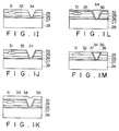
type silicon layer 32 is epitaxially grown on the upper surface of the p-type silicon layer 29 and the high concentration n-type silicon layer 31. Namely, trichlorosilan (SiHCℓ₃) gas is thus used to epitaxially grow a low concentration n-type silicon layer 32 having a layer thickness of 15 µm, and a resistivity of 7 to 9 Ω/cm at 1140°C. - In FIG. 1H, a resist
layer 33 where a predetermined pattern is formed is formed on the upper surface of the low concentration n-type silicon layer 32 by using well known means. - In FIG. 1I, the low concentration n-
type silicon layer 32, the p-type silicon layer 29, and the high concentration p-type silicon layer 26 are etched from the upper surface down to the upper portion of the insulatingfilm 27 by using KOH-system etchant to form a V-groove 34 thereafter to remove the resistlayer 33. - In FIG. 1J, the side wall surfaces of the
V groove 34 and the upper surface of the low concentration n-type silicon layer 32 are thermally oxidized to form an insulating film (dielectric film) 35 of SiO₂ having a thickness of 1 µm. - In FIG. 1K, a
polycrystalline silicon layer 36 is deposited on the entire upper surface portion of the insulatingfilm 35 on the low concentration n-type silicon layer 32 so that the internal portion of theV groove 34 on which the insulatingfilm 35 is formed is completely filled with thesilicon layer 36. Namely, SiHCℓ₃ gas is used to deposit thepolycrystalline silicon layer 36 having a layer thickness of 80 µm by using CVD process, etc. at 1100°C. - In FIG. 1L, rough grinding processing is carried out in a horizontal direction by means of grinder, etc. until the layer thickness of the
polycrystalline layer 36 on theinsulation film 35 formed on the low concentration n-type silicon layer 32 becomes equal to 10 µm. This processing is implemented to such an extent that the internal unevenness of the thickness of thepolycrystalline silicon layer 36 at this time is 5 µm or less. - Thereafter, the surface of the
polycrystalline silicon layer 36 roughly ground is subjected to mirror polishing processing, e.g., by mechano-chemical polishing used in mirror polishing processing for an ordinary silicon substrate. This mirror polishing processing is carried out until thepolycrystalline silicon layer 36 on the insulatingfilm 35 is removed (FIG. 1M). - In this polishing processing, the polishing condition where the polishing rate ratio (selection ratio) of the polycrystalline silicon to the silicon dioxide is 1/5 or less is preferably used. The reason why such a condition is employed is based on the following finding. Namely, a polycrystalline silicon layer is deposited on a silicon dioxide film having a thickness of 1 µm on a silicon substrate. Then, rough grinding is implemented to the upper surface of the polycrystalline silicon layer so that the internal unevenness is 5 µm or less. Mirror-polishing processing is implemented from the side of the polycrystalline silicon layer subjected to rough grinding as stated above by using respective polishing conditions where the polishing rate ratios are different. The yield in the case where processing can be carried out in a manner that the silicon substrate of the underlying layer is not exposed at this time is experimentally determined. In this embodiment, the above-mentioned condition is determined from this finding. Namely, as shown by the graph of FIG. 2 in which the polishing rate ratio between silicon dioxide and polycrystalline silicon is taken on the abscissa and the processing yield is taken on the ordinate, when the polishing rate ratio is 1/5 or less, the polycrystalline silicon layer is entirely removed before the silicon substrate of the underlying layer is exposed, so the processing yield is at a high level of substantially 100%. In contrast, when the polishing rate ratio is above 1/5, silicon dioxide film is partially removed before the polycrystalline layer is entirely removed, so the silicon substrate of the underlying layer will be exposed and polished. Since whether or not the polycrystalline silicon layer is entirely removed can be easily discriminated at the processing step, the polishing rate ratio is set to a value less than 1/5. If such a condition is satisfied, it is possible to precisely determine the end point of polishing by control of time.
- Such a polishing rate ratio is greatly influenced by the kind of the polishing material, but processing pressure and/or rotation speed in the polishing machine are also an important factor for the polishing rate ratio. Accordingly, it is necessary to select the polishing condition where these factors are synthetically taken into consideration.
- In FIG. 1M, the insulating
film 35 on the low concentration n-type silicon layer 32 is removed by using hydrogen fluoride (HF). - Thus, there is formed an isolation section of the dielectric isolation structure in which insulating
films V groove 34 and thepolycrystalline silicon layer 36 is formed within theV groove 34. - By undergoing the above-mentioned process steps, a semiconductor substrate in which the low concentration n-
type silicon layer 32 having a predetermined layer thickness, or the like is formed is provided. By using this semiconductor substrate, elements are formed as shown in FIG. 4. - The low concentration n-
type silicon layer 32 thus obtained is featured below. Namely, because a layer formed on the p-type silicon layer 29 subjected to mirror-polishing processing, with good flatness and in a manner that the thickness thereof is uniformly and precisely controlled is used as it is, the layer thickness of the low concentration n-type silicon layer 32 thus obtained is uniform and accurate. - Furthermore, in order to experimentally confirm this, the thickness of the low concentration n-
type silicon layer 32 and the internal unevenness thereof are measured in connection with 50 semiconductor substrates provided by undergoing the above-mentioned process steps. The measured result is shown at the left hand side of FIG. 3 in which the internal unevenness is taken on the abscissa and frequency is taken on the ordinate. As seen from the comparison with the case of the prior art, in accordance with semiconductor substrates according to this embodiment, the internal unevenness thereof is 1.5 µm (+ 5%) or less even if attention is drawn to semiconductor substrates for which the internal unevenness is large. This satisfies the level in which the required internal unevenness is less than + 5%. Furthermore, the mean value of the distribution of internal unevenness values is 0.94 µm (+ 3.13%) and there is less unevenness. - In addition, in accordance with the method according to this method, in order to form the low concentration n-
type silicon layer 32 having a layer thickness of 15 µm, it is unnecessary to additionally and thickly grow the epitaxial layer by taking particularly a machining clearance for grinding or polishing at the subsequent process steps into consideration. Namely, it is sufficient to carry out epitaxial growth just by a predetermined thickness of 15 µm, resulting in no possibility that the cost is increased. - It should be noted that this invention is not limited to the above-described embodiment, but may be carried out in a manner that it can be suitably modified or changed within the range which does not depart from the gist of the invention.
- Reference signs in the claims are intended for better understanding and shall not limit the scope.
Claims (3)
- A method of manufacturing a semiconductor substrate comprising:
a first step of bonding first and second semiconductor substrates (25, 28) in a manner that a first dielectric film (27) formed on at least one surface of said semiconductor substrates is placed therebetween,
a second step of polishing the surface of said bonded first semiconductor substrate to decrease the thickness of said first semiconductor substrate thus to form a first semiconductor layer (29) having a predetermined thickness,
a third step of forming a second semiconductor layer (32) having a predetermined thickness on said first semiconductor layer by epitaxial growth,
a fourth step of forming, in said first and second semiconductor layers, a groove (34) having a depth from the surface of said second semiconductor layer down to said first dielectric film to form a second dielectric film on the side surfaces of said groove and the upper surface of said second semiconductor layer,
a fifth step of completely filling a filler (36) into said grooves and depositing said filler on said second dielectric film,
a sixth step of polishing and removing said filler by using the polishing condition where the ratio between the polishing rate for said second dielectric film and the polishing rate for said filler is less than 1/5, to thus allow said second dielectric film on said second semiconductor layer to be exposed, and
a seventh step of removing said second dielectric film on said second semiconductor layer exposed at said sixth step. - A method of manufacturing a semiconductor substrate as set forth in claim 1, wherein said filler is polysilicon.
- A method of manufacturing a semiconductor substrate as set forth in claim 1, which further comprises a step of forming a buried layer (26) between said first and second semiconductor substrates.
Applications Claiming Priority (3)
| Application Number | Priority Date | Filing Date | Title |
|---|---|---|---|
| JP33670690 | 1990-11-30 | ||
| JP2336706A JP2925312B2 (en) | 1990-11-30 | 1990-11-30 | Semiconductor substrate manufacturing method |
| JP336706/90 | 1990-11-30 |
Publications (3)
| Publication Number | Publication Date |
|---|---|
| EP0488230A2 true EP0488230A2 (en) | 1992-06-03 |
| EP0488230A3 EP0488230A3 (en) | 1993-02-03 |
| EP0488230B1 EP0488230B1 (en) | 2000-05-03 |
Family
ID=18301953
Family Applications (1)
| Application Number | Title | Priority Date | Filing Date |
|---|---|---|---|
| EP91120294A Expired - Lifetime EP0488230B1 (en) | 1990-11-30 | 1991-11-27 | Method of manufacturing a semiconductor substrate having a dielectric isolation structure |
Country Status (5)
| Country | Link |
|---|---|
| US (1) | US5352625A (en) |
| EP (1) | EP0488230B1 (en) |
| JP (1) | JP2925312B2 (en) |
| KR (1) | KR950003899B1 (en) |
| DE (1) | DE69132157T2 (en) |
Cited By (1)
| Publication number | Priority date | Publication date | Assignee | Title |
|---|---|---|---|---|
| WO1998013878A1 (en) * | 1996-09-23 | 1998-04-02 | Siemens Aktiengesellschaft | Self-aligned non-volatile storage cell |
Families Citing this family (6)
| Publication number | Priority date | Publication date | Assignee | Title |
|---|---|---|---|---|
| EP0612438A1 (en) * | 1991-11-15 | 1994-08-31 | Analog Devices, Inc. | Process for fabricating insulation-filled deep trenches in semiconductor substrates |
| US5561073A (en) * | 1992-03-13 | 1996-10-01 | Jerome; Rick C. | Method of fabricating an isolation trench for analog bipolar devices in harsh environments |
| JPH10209293A (en) * | 1997-01-22 | 1998-08-07 | Sony Corp | Manufacture of semiconductor device |
| US6080042A (en) * | 1997-10-31 | 2000-06-27 | Virginia Semiconductor, Inc. | Flatness and throughput of single side polishing of wafers |
| KR100905470B1 (en) | 2002-11-20 | 2009-07-02 | 삼성전자주식회사 | Thin film transistor array panel |
| US20070042563A1 (en) * | 2005-08-19 | 2007-02-22 | Honeywell International Inc. | Single crystal based through the wafer connections technical field |
Citations (3)
| Publication number | Priority date | Publication date | Assignee | Title |
|---|---|---|---|---|
| US3979237A (en) * | 1972-04-24 | 1976-09-07 | Harris Corporation | Device isolation in integrated circuits |
| US4948742A (en) * | 1987-09-08 | 1990-08-14 | Mitsubishi Denki Kabushiki Kaisha | Method of manufacturing a semiconductor device |
| EP0398468A2 (en) * | 1989-05-16 | 1990-11-22 | Kabushiki Kaisha Toshiba | Dielectrically isolated substrate and semiconductor device using the same |
Family Cites Families (2)
| Publication number | Priority date | Publication date | Assignee | Title |
|---|---|---|---|---|
| US4255207A (en) * | 1979-04-09 | 1981-03-10 | Harris Corporation | Fabrication of isolated regions for use in self-aligning device process utilizing selective oxidation |
| US5049968A (en) * | 1988-02-08 | 1991-09-17 | Kabushiki Kaisha Toshiba | Dielectrically isolated substrate and semiconductor device using the same |
-
1990
- 1990-11-30 JP JP2336706A patent/JP2925312B2/en not_active Expired - Fee Related
-
1991
- 1991-11-27 DE DE69132157T patent/DE69132157T2/en not_active Expired - Fee Related
- 1991-11-27 EP EP91120294A patent/EP0488230B1/en not_active Expired - Lifetime
- 1991-11-29 KR KR1019910021681A patent/KR950003899B1/en not_active IP Right Cessation
- 1991-11-29 US US07/800,074 patent/US5352625A/en not_active Expired - Lifetime
Patent Citations (3)
| Publication number | Priority date | Publication date | Assignee | Title |
|---|---|---|---|---|
| US3979237A (en) * | 1972-04-24 | 1976-09-07 | Harris Corporation | Device isolation in integrated circuits |
| US4948742A (en) * | 1987-09-08 | 1990-08-14 | Mitsubishi Denki Kabushiki Kaisha | Method of manufacturing a semiconductor device |
| EP0398468A2 (en) * | 1989-05-16 | 1990-11-22 | Kabushiki Kaisha Toshiba | Dielectrically isolated substrate and semiconductor device using the same |
Non-Patent Citations (1)
| Title |
|---|
| RESEARCH DISCLOSURE no. 306, 1989, HAVANT GB page 743 'METHOD FOR PRODUCING PLANARIZED POLYYSILICON FILLED TRENCHES DISCLOSURE NO 30670' * |
Cited By (1)
| Publication number | Priority date | Publication date | Assignee | Title |
|---|---|---|---|---|
| WO1998013878A1 (en) * | 1996-09-23 | 1998-04-02 | Siemens Aktiengesellschaft | Self-aligned non-volatile storage cell |
Also Published As
| Publication number | Publication date |
|---|---|
| KR950003899B1 (en) | 1995-04-20 |
| US5352625A (en) | 1994-10-04 |
| DE69132157D1 (en) | 2000-06-08 |
| JPH04206757A (en) | 1992-07-28 |
| EP0488230A3 (en) | 1993-02-03 |
| DE69132157T2 (en) | 2000-11-23 |
| JP2925312B2 (en) | 1999-07-28 |
| EP0488230B1 (en) | 2000-05-03 |
Similar Documents
| Publication | Publication Date | Title |
|---|---|---|
| US4851078A (en) | Dielectric isolation process using double wafer bonding | |
| US4601779A (en) | Method of producing a thin silicon-on-insulator layer | |
| US4897362A (en) | Double epitaxial method of fabricating semiconductor devices on bonded wafers | |
| EP0977255B1 (en) | A method of fabricating an SOI wafer and SOI wafer fabricated by the method | |
| US4729006A (en) | Sidewall spacers for CMOS circuit stress relief/isolation and method for making | |
| EP0036111A2 (en) | Method for making fine deep dielectric isolation | |
| EP0601950A2 (en) | Method of producing a thin silicon-on-insulator layer | |
| JPH0344419B2 (en) | ||
| JPH0834261B2 (en) | SOI structure for BICMOS integrated circuit and method of manufacturing the same | |
| US3979237A (en) | Device isolation in integrated circuits | |
| JPS6113642A (en) | Method of forming separate region of semiconductor substrate | |
| US5420064A (en) | Method of manufacturing a dielectric isolation substrate | |
| US4408386A (en) | Method of manufacturing semiconductor integrated circuit devices | |
| US4554059A (en) | Electrochemical dielectric isolation technique | |
| EP0488230B1 (en) | Method of manufacturing a semiconductor substrate having a dielectric isolation structure | |
| US3954522A (en) | Integrated circuit process | |
| KR940003217B1 (en) | Semiconductor device and making method thereof | |
| EP0418737B1 (en) | Method of manufacturing a semiconductor substrate dielectric isolating structure | |
| US6617646B2 (en) | Reduced substrate capacitance high performance SOI process | |
| US4026736A (en) | Integrated semiconductor structure with combined dielectric and PN junction isolation including fabrication method therefor | |
| EP0469583A2 (en) | Semiconductor substrate with complete dielectric isolation structure and method of making the same | |
| EP0547677A2 (en) | Use of vapor-phase etching in fabrication of semiconductor-on-insulator structure | |
| GB2137019A (en) | Semiconductor Device and Method for Manufacturing | |
| US5213993A (en) | Method of manufacturing semiconductor substrate dielectric isolating structure | |
| US5677564A (en) | Shallow trench isolation in integrated circuits |
Legal Events
| Date | Code | Title | Description |
|---|---|---|---|
| PUAI | Public reference made under article 153(3) epc to a published international application that has entered the european phase |
Free format text: ORIGINAL CODE: 0009012 |
|
| 17P | Request for examination filed |
Effective date: 19911127 |
|
| AK | Designated contracting states |
Kind code of ref document: A2 Designated state(s): DE FR GB |
|
| PUAL | Search report despatched |
Free format text: ORIGINAL CODE: 0009013 |
|
| AK | Designated contracting states |
Kind code of ref document: A3 Designated state(s): DE FR GB |
|
| 17Q | First examination report despatched |
Effective date: 19930402 |
|
| GRAG | Despatch of communication of intention to grant |
Free format text: ORIGINAL CODE: EPIDOS AGRA |
|
| GRAG | Despatch of communication of intention to grant |
Free format text: ORIGINAL CODE: EPIDOS AGRA |
|
| GRAH | Despatch of communication of intention to grant a patent |
Free format text: ORIGINAL CODE: EPIDOS IGRA |
|
| GRAH | Despatch of communication of intention to grant a patent |
Free format text: ORIGINAL CODE: EPIDOS IGRA |
|
| GRAA | (expected) grant |
Free format text: ORIGINAL CODE: 0009210 |
|
| AK | Designated contracting states |
Kind code of ref document: B1 Designated state(s): DE FR GB |
|
| REF | Corresponds to: |
Ref document number: 69132157 Country of ref document: DE Date of ref document: 20000608 |
|
| ET | Fr: translation filed | ||
| PLBE | No opposition filed within time limit |
Free format text: ORIGINAL CODE: 0009261 |
|
| STAA | Information on the status of an ep patent application or granted ep patent |
Free format text: STATUS: NO OPPOSITION FILED WITHIN TIME LIMIT |
|
| 26N | No opposition filed | ||
| REG | Reference to a national code |
Ref country code: GB Ref legal event code: IF02 |
|
| PGFP | Annual fee paid to national office [announced via postgrant information from national office to epo] |
Ref country code: FR Payment date: 20021108 Year of fee payment: 12 |
|
| PGFP | Annual fee paid to national office [announced via postgrant information from national office to epo] |
Ref country code: GB Payment date: 20021127 Year of fee payment: 12 |
|
| PG25 | Lapsed in a contracting state [announced via postgrant information from national office to epo] |
Ref country code: GB Free format text: LAPSE BECAUSE OF NON-PAYMENT OF DUE FEES Effective date: 20031127 |
|
| GBPC | Gb: european patent ceased through non-payment of renewal fee |
Effective date: 20031127 |
|
| PG25 | Lapsed in a contracting state [announced via postgrant information from national office to epo] |
Ref country code: FR Free format text: LAPSE BECAUSE OF NON-PAYMENT OF DUE FEES Effective date: 20040730 |
|
| REG | Reference to a national code |
Ref country code: FR Ref legal event code: ST |
|
| PGFP | Annual fee paid to national office [announced via postgrant information from national office to epo] |
Ref country code: DE Payment date: 20051124 Year of fee payment: 15 |
|
| PG25 | Lapsed in a contracting state [announced via postgrant information from national office to epo] |
Ref country code: DE Free format text: LAPSE BECAUSE OF NON-PAYMENT OF DUE FEES Effective date: 20070601 |