EP0488077B1 - Progressive scan television system using luminance low frequencies from previous field - Google Patents
Progressive scan television system using luminance low frequencies from previous field Download PDFInfo
- Publication number
- EP0488077B1 EP0488077B1 EP91119948A EP91119948A EP0488077B1 EP 0488077 B1 EP0488077 B1 EP 0488077B1 EP 91119948 A EP91119948 A EP 91119948A EP 91119948 A EP91119948 A EP 91119948A EP 0488077 B1 EP0488077 B1 EP 0488077B1
- Authority
- EP
- European Patent Office
- Prior art keywords
- signal
- output
- line
- motion
- sub
- Prior art date
- Legal status (The legal status is an assumption and is not a legal conclusion. Google has not performed a legal analysis and makes no representation as to the accuracy of the status listed.)
- Expired - Lifetime
Links
Images


Classifications
-
- H—ELECTRICITY
- H04—ELECTRIC COMMUNICATION TECHNIQUE
- H04N—PICTORIAL COMMUNICATION, e.g. TELEVISION
- H04N3/00—Scanning details of television systems; Combination thereof with generation of supply voltages
- H04N3/10—Scanning details of television systems; Combination thereof with generation of supply voltages by means not exclusively optical-mechanical
- H04N3/28—Scanning details of television systems; Combination thereof with generation of supply voltages by means not exclusively optical-mechanical producing multiple scanning, i.e. using more than one spot at the same time
-
- H—ELECTRICITY
- H04—ELECTRIC COMMUNICATION TECHNIQUE
- H04N—PICTORIAL COMMUNICATION, e.g. TELEVISION
- H04N7/00—Television systems
- H04N7/01—Conversion of standards, e.g. involving analogue television standards or digital television standards processed at pixel level
- H04N7/0117—Conversion of standards, e.g. involving analogue television standards or digital television standards processed at pixel level involving conversion of the spatial resolution of the incoming video signal
- H04N7/012—Conversion between an interlaced and a progressive signal
-
- H—ELECTRICITY
- H04—ELECTRIC COMMUNICATION TECHNIQUE
- H04N—PICTORIAL COMMUNICATION, e.g. TELEVISION
- H04N5/00—Details of television systems
- H04N5/44—Receiver circuitry for the reception of television signals according to analogue transmission standards
- H04N5/57—Control of contrast or brightness
Definitions
- This invention relates to television systems of a type in which interlaced video input signals are converted to a non-interlaced or "progressively scanned” form for display.
- patent US-A-4,400,719 entitled TELEVISION DISPLAY SYSTEM WITH REDUCED LINE-SCAN ARTIFACTS which issued August 23, 1983.
- Other examples include the system described by Fujimura et al. in U.S. patent US-A-4,509,071 entitled DOUBLE SCANNING NON-INTERLACE TELEVISION RECIEVER which issued April 2, 1985 and the system described by Okada et al. in U.S. patent US-A-4,451,848 entitled TELEVISION RECEIVER INCLUDING A CIRCUIT FOR DOUBLING LINE SCANNING FREQUENCY which issued May 29, 1984.
- motion adaptive a motion detector is used to switch between the two basic types of processors as a function of motion. For example, when the incoming video signal represents a still image the signal is processed by a field type processor which generates extra lines for display by interleaving the currently received lines with lines of a previous field. Conversely, when the incoming video signal represents a moving image, the extra lines for display are obtained by interpolation (or repeating) lines of the currently received field.
- a problem characteristic of motion adaptive systems is that the memory requirements for providing motion detection are far greater than the requirements for merely providing field progressive scan processing when motion detection is implemented in the usual way by comparing video signals delayed by one full frame.
- One approach to avoiding the requirement for a full frame of memory is to detect motion by measurement of the video signal sideband energy.
- An example of such a system is described by D. H. Pritchard in US patent 4,641,186 entitled MOTION DETECTOR THAT EXTRACTS MOTION INFORMATION FROM SIDEBANDS OF A BASEBAND TELEVISION SIGNAL which issued February 1987.
- the sideband energy motion detection method is, however, relatively complicated.
- the present invention resides in part in the recognition of the need for a progressive scan system which effectively avoids the foregoing problems while retaining the advantages of each of the earlier solutions.
- the invention provides an apparatus as claimed in claim 1.
- Progressive scan conversion apparatus embodying the invention includes a source for providing a video input signal of a given line rate.
- a processor coupled to the source, provides a video difference signal representative of a difference between a first low frequency component derived from a current line of said video input signal and a second low frequency component derived from at least one previous line of the video input signal.
- An output circuit time compresses and combines the video difference and input signals and forms a progressive scan output signal.
- the output circuit includes circuit means for doubling the line rate of the video difference signal, for doubling the line rate of the video input signal and for adding a line of the double line-rate video difference signal to every other line of the double line-rate video input signal for forming said progressive scan output signal.
- the video input signal is of digital form
- the processor includes means for sub-sampling the video input signal prior to forming the video difference signal
- the output circuit includes means for up-sampling the video difference signal prior to the addition of the double line-rate video signals to form the progressive scan output signal.
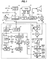
- the television receiver 10 of FIGURE 1 includes a progressive scan processor 30 (outlined in phantom) comprising an input unit 30A (outlined in phantom) and an output unit 30B (outlined in phantom).
- the input unit 30A provides a video difference signal (Y12) representative of a difference between a first low frequency component (Y6) derived from a current line of a video input signal (Y3) and a second low frequency component (Y10) derived from at least one previous line of the video input signal (Y3).
- the output unit 30B processes the video difference signal (Y12) and the video input signal (Y3), as will be explained, to form a progressive scan luminance output signal (Y2) of double the line rate of the input signal.
- the combination of the input (30A) and output (30B) units of the progressive scan processor (30A,30B) provide a progressive scan output signal (Y2) having the relatively high vertical resolution characteristic of field progressive scan systems; having the motion artifact immunity characteristic of line progressive scan systems; having the motion adaptability characteristic of motion adaptive systems; and having substantially reduced system memory requirements as compared with conventional motion adaptive systems.
- the system provides "dual band" video processing without requiring the use of conventional complementary high pass and low pass filters for band splitting.
- the receiver 10 of FIGURE 1 comprises a luminance-chrominance signal separation circuit 12 which separates a composite video input signal S1 into a luminance component Y1 and a chrominance component C1.
- the input video signal S1 may be provided by a conventional tuner, IF amplifier and detector unit 14 from an antenna or cable input 16 or, alternatively, it may be provided by an auxiliary input terminal 18 or some other suitable source.
- Separation circuit 12 may be of conventional design such as a comb filter or a combination of high and low pass filters as is well known.
- the separated chrominance signal component C1 is applied to a speed-up unit 20 which time compresses and repeats each line thereof to provide a chrominance output signal C2 having double the line rate of the video input signal and in which each line is repeated. Examples of suitable "speed-up" circuits are described later.
- the luminance signal Y1 is converted to digital form by means of an analog-to-digital (A/D) converter 13 and the digitized luminance signal Y3 is applied to a luminance signal progressive scan processor 30 (outlined in phantom) which generates a motion adaptive double line-rate progressively scanned luminance output signal Y2 as will be described.
- A/D analog-to-digital
- a luminance signal progressive scan processor 30 (outlined in phantom) which generates a motion adaptive double line-rate progressively scanned luminance output signal Y2 as will be described.
- This signal is converted back to analog form (Y5) by means of a digital to analog (D/A) converter 23 and the double line-rate signals C2 and Y5 are applied to a conventional luminance-chrominance signal processing unit 24 which provides such functions as color demodulation, brightness and contrast control and color matrixing so as to provide a progressively scanned output signal S2 of a form (e.g., RGB component form) suitable for display by a kinescope 26 or some other suitable display device (e.g., an LCD device or a projection display).
- a form e.g., RGB component form
- the images produced by kinescope 26 have twice as many lines as the input signal whereby the visibility of raster line structure is substantially reduced as compared with conventional interlaced images.
- Clock signals CL for converters 13 and 23 are provided by a timing signal generator 21.
- This generator may comprise a phase locked loop (PLL) generator of conventional design locked to a multiple of the color burst component of the input signal S1 or locked to a multiple of the line frequency of the input signal S1.
- PLL phase locked loop
- Typical sampling clock frequencies are three or four times the frequency of the color subcarrier for systems employing what is commonly called “burst locked” clocking.
- the timing signal generator 21 is phase locked to a multiple of the horizontal line rate. This is commonly called “line locked” clock generation and has an advantage over burst locking in that the system is usable with so-called non-standard video sources where the relationship between line and burst frequencies may vary.
- the clock frequency CL is selected to be 1024 times the horizontal line rate of the video input signal.
- this frequency CL is about 16.1 mega-Hz.
- Other clock signals provided by timing unit 21 include CL/4 and 2CL which are used for sample rate conversions as will be explained. Unit 21 also provides horizontal and vertical line rate frequencies used for deflection purposes.
- FIGURE 1 comprises the progressive scan processor 30 that provides the motion adaptively processed progressively scanned luminance output signal Y2.
- the motion adaptive components of Y2 are derived by processing only sub-sampled low frequency components of the luminance signal Y3.
- restricting the processing in this manner greatly reduces the amount of memory required for implementing line, field and frame delays necessary for motion adaptive processing as compared with processing of full bandwidth signals.
- a further advantage relates to the use of "differential" processing (i.e., processing of signal differences rather than absolute values).
- Differential processing eliminates the need for special high pass and low pass filters having matched amplitude and phase response characteristics that are required in conventional split-band processing systems as previously described. Such high pass and low pass filters having truly complementary amplitude and phase characteristics are complex and expensive.
- the progressive scan processor 30 is divided, by phantom lines, into two portions comprising an input circuit 30A and an output circuit 30B.
- the full bandwidth luminance signal Y3 is applied to a sub-sampling circuit 40 by means of a low pass filter 37.
- Sub-sampling unit 40 is clocked at a rate of CL/4 and greatly reduces the luminance signal data rate and thus reduces the number of bytes of memory required for implementing video delay functions.
- CL/4 the rate of CL/4
- the full bandwidth luminance signal is digitized at a the assumed clock rate of (about) 16 MHz and then sub-sampled at a 4 MHz clock rate then only one-quarter of the memory will be needed to implement the same digital delay as would be required if the signal were not sub-sampled.
- select other clock rates and sub-sampling rates in a specific application of the principles of the invention.
- the sub-sampled signal is low pass filtered prior to sub-sampling and this function is provided by low pass filter 37.
- a suitable cut-off frequency for filter 37 is about one-half of the sub-sampling rate (e.g., about 2 MHz for the assumed sub-sampling rate of about 4 MHz.) In practice, it is desirable that the filter cut-off frequency be slightly lower than half the sub-sampling rate to allow for the finite slope of the filter response in the transition region between the filter pass band and the filter stop band.
- An exemplary cut-off frequency, for the assumed sampling frequency. is about 1.5 MHz for 6 dB of attenuation at band edge.
- This frequency is well below the Nyquist rate of 2.0 MHz for the assumed sampling rate of about 4 MHz.
- this reduces the number of filter elements needed to implement the anti-aliasing low pass filter 37.
- proportionally higher anti-aliasing filter cut-off frequencies may be used.
- the sub-sampled and low-pass filtered luminance signal Y6 is applied to the inputs of a tapped frame delay unit 42, a motion detector 44, an averager 45 and a subtractor 48.
- Delay unit 42 has output taps providing a one-line (1-H) delayed luminance signal Y7, a one field delayed (263 H) delayed luminance signal Y9 and a frame (525H) delayed luminance signal Y11.
- the field delay would be 313 lines and the frame delay would be 625 lines.
- the one line (1-H) delayed output tap of delay unit 42 is connected to the other input of averager 46 which provides a line averaged output signal Y8.
- a "soft switch” 50 combines the averaged luminance signal Y8 with a field delayed luminance signal Y9 to provide a combined or "blended" luminance output signal Y10 in which the proportions of the Y8 and Y9 components are controlled by motion detector 44 and a control signal generator 46.
- Motion detector 44 has one input connected to receive the non-delayed luminance signal Y6. It has a second input connected to receive a frame delayed luminance signal Y11 provided by delay unit 42 and provides a motion indicating signal M representative of the difference between signals Y6 and Y11.
- a suitable motion detector is shown and described later.
- control signal generator 46 is to convert the motion signal M, which is linearly related to motion, to a control signal K which is non-linearly related to motion so as to provide a better match to the motion sensitivity of the human visual system. Examples of suitable control signal generators are shown and described later.
- the resultant "motion adapted" luminance signal Y10 provided by soft switch 50 is applied to the second input of subtractor 48 which receives the non-delayed, sub-sampled and low-pass filtered luminance signal Y6 at its other input and provides a luminance output difference signal Y12.
- the signal Y12 is a video difference signal representative of a difference between a first low frequency component (Y6) derived from a current line of the video input signal and a second low frequency component (Y10) derived from at least one previous line of the video input signal.
- the output circuit 30B of progressive scan processor 30 selectively combines the video difference signal (Y12) with the full bandwidth video input signal Y3 to form the progressive scan video output signal Y2.
- the full bandwidth luminance signal Y3 is applied to a speed-up unit 36 which time compresses and repeats each line thereof to provide a double line-rate luminance output signal Y4 in which each line is time compressed by a factor of two and repeated.
- the difference signal Y12 produced by subtractor 48 is applied to a luminance signal speed-up unit 54 that time compresses each line thereby doubling the line rate of the difference signal Y12.
- Doubling the line rate of the sub-sampled signal Y12 also doubles the sample rate (e.g., from 4 to 8 MHz for the assumed clock) of the speeded up signal Y13.
- the sample rate of signal Y13 is then applied to a sample rate converter ("UP SAMPLE") 56 that quadruples the sample rate of the time compressed signal Y13.
- UP SAMPLE sample rate converter
- This sample rate conversion may be implemented by repeating samples or by interpolating samples. Accordingly, for the assumed clock and sub-sampling values, the processed low frequency difference signal Y14 at the output of "up-sample” converter 56 equals about 32 MHz which equals the sample rate of the speeded-up broad band luminance signal Y4.
- the sample rate equalization or "matching" of the processed luminance signal lows (Y14) and the full bandwidth luminance signal (Y4) allows the direct addition of these signals in adder 38 to form the luminance progressive scan signal Y2.
- the last step, prior to the addition, is to apply signal Y14 to a switch 57 which is synchronized with the line frequency so as to modify every other line of the processed signal Y4 to produce the progressive scan output signal Y2.
- FIGURE 1 In the embodiment of FIGURE 1 described thus far there has been shown and described a progressive scan processor 30 having a number of features which include: (1) motion artifacts are minimized by motion adaptive processing provided by switch 50 which selects line averaged or field delayed signals as a function of motion; (2) memory requirements are substantially reduced by processing sub-sampled low frequency luminance components taken from the present line and a selected previous line; and (3) the processed output signal is formed by combining processed low frequency difference components with the full bandwidth luminance signal.
- This latter feature completely eliminates the need for complementary high pass and low pass filters having matched amplitude and phase responses as would otherwise be required if the luminance signal band were to be "split" or divided into high-pass and low-pass components for processing of the signal.
- Subtractor 48 will thus subtract the field delayed low frequency component Y9 from the current low frequency component Y6 to provide the difference signal Y12.
- Adder 38 will then add one line of the speeded up and sample rate converted difference signal Y14 (selected by switch 57) to every other line of the speeded up full bandwidth luminance signal Y4 to form the progressive scanned luminance output signal Y2.
- the luminance signal will comprise two components in different frequency bands even though the system employs no high pass filters.
- a first component taken from a currently received line, will equal a high frequency component of the full bandwidth signal Y3 for frequencies above the cut-off frequency of low pass filter 37.
- a second component will equal a low frequency component, selected by filter 37, taken from the previous field. This may be understood by considering that the difference signal Y12 actually comprises two low frequency components (Y6 and Y10) and the phase of a selected one of these components (Y6) is reversed due to the subtraction.
- the output signal Y2 equals the full bandwidth luminance signal Y3, minus the low frequency component of Y3 passed by filter 37, plus the low frequency component of Y3 passed by filter 37 but taken from the previous field.
- the low frequency components of the current line of signal Y3 simply cancel out because they are out of phase.
- the missing lows due to the cancellation are replaced by the lows from the previous field (Y10). Since high frequency components of signal Y3 are not processed in processor 30A these components of Y3 are not disturbed and form the high frequency component of the output signal Y2.
- alternate lines of the output signal Y2 comprise the full bandwidth luminance signal Y3 and the in-between or "interstitial" lines comprise a high frequency component (above the cut-off frequency of filter 37) taken from the currently received line (Y3) and a low frequency component (9) taken from the previous field.
- low frequency video components that are displayed will exhibit the full vertical resolution of a complete video frame.
- the effect is to increase the vertical resolution of displayed still images as compared with standard interlaced images.
- the soft switch 50 selects only the line averaged low frequency luminance signal Y8 so that the low frequency difference signal Y12 equals the difference between the low frequency component Y6 of a current line and the average Y8 of the low frequency components of the current and a previous line.
- the resultant sum signal (for every other line) comprises a low frequency component equal to the average of the current and previous lines and a high frequency component taken from the current line. For the remaining lines the output equals the current line.
- switch 50 blends the line averaged signal Y8 and the field delayed signal Y9 to form the signal Y10 which after subtraction of signal Y6 forms the difference signal Y12.
- the output signal Y2 includes a high frequency component derived from the currently received line and a low frequency component derived (by motion dependent blending in switch 50) from two lines of the current field or one line of a previous field depending on the degree of the image motion.
- the difference signal Y12 was formed by subtracting Y6 from Y10 and that this resulted in a reversal of the phase of the current low frequency component Y6 relative to the phase of the full bandwidth signal Y6 to thereby cancel these components when they are later combined by addition in adder 38.
- the signal Y10 may be subtracted from Y6 to form the difference signal Y12 along with modifying the output circuit 30B as will now be described.
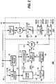
- FIGURE 2 illustrates a modification of the progressive scan processor 30 of FIGURE 1 wherein the inputs to subtractor 48 are reversed in input circuit 30A and in output circuit 30B the adder 38 is replaced by a subractor 39 that subtracts every other line of signal Y14 from the full bandwidth luminance signal Y4.
- This embodiment of the invention is functionally identical to that of FIGURE 1 and is structurally identical except for the two noted changes.
- signal Y6 was subtracted from signal Y10 to form the low frequency difference signal Y12.
- signals Y12 and Y3 resulted in an output signal Y2 having high frequency components taken from the current line and low frequency components derived from the previous line or field.
- FIGURE 2 the same result is obtained when the inputs of subtractor 48 in input circuit 30A are reversed by replacing the adder 38 in output circuit 30B with a subtractor 39.
- FIGURE 1 it does not make a functional difference if one subtracts Y6 from Y10 and later adds signals Y14 and Y4 (as in FIGURE 1) or if one subtracts signal Y10 from Y6 and later subtracts signal Y14 from Y4 as in FIGURE 3.
- the example of FIGURE 1 is presently preferred because it requires only one subtractor (rather than two) and thus requires less hardware for implementation since addition is less complicated in digital processing than subtraction.
- the example of FIGURE 1 has the technical advantage as well of providing higher reliability as there are fewer parts to fail.
- FIGURE 3 illustrates a modification of the output circuit 30A of progressive scan processor 30 wherein the positions of the sample rate converter ("up-sample") circuit 54 and the speed-up circuit 56 are reversed in the cascade connection of these two circuit elements. To effect this change all that is required is an appropriate selection of the various clock frequencies.
- the speed-up circuit for example requires a read clock that is twice the write clock frequency and the sample rate conversion requires a read clock that is four times the write clock frequency.
- the speed-up circuit receives a write clock frequency of CL/4 (e.g., 4 MHz) and a read clock frequency of CL/2 (e.g., 8 MHz) and the sample rate converter receives a write clock frequency of CL/2 (e.g., 8 MHz) and a read clock frequency of 2CL (e.g., 32 MHz).
- the clock frequencies are changed as follows: (1) the write and read clocks for speed-up are changed to CL and 2CL, respectively, (e.g., 16 and 32 MHz) and (2) the write and read clocks for sample rate conversion are changed to CL/4 and CL, respectively (e.g., about 4 and 16 MHz).
- the overall operation of the speed-up and sample rate converters provides exactly the same result as in the example of FIGURE 1 in that the sub-sampled difference signal Y12, after sample rate conversion and speed-up, is of the same line rate and sample rate as the speeded up full bandwidth luminance signal Y3 and so these signals may be combined (by addition as in FIG. 1 or by subtraction as in FIG. 2) to provide the progressively scanned output signal Y2.
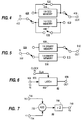
- FIGURES 4 and 5 are exemplary of "speed-up" circuits suitable for doubling the line rate of chrominance or luminance input signals in the receiver of FIGURE 1.
- video signals to be "speeded-up" at input 402 are alternately applied via a line rate operated “write” switch 404 to a pair of one line (1H) CCD memories 406 and 408.
- the other memory is "read” at double the write clock rate and coupled to an output 412 via a read switch 410. Since the read clock rate is twice the write clock rate the input signal is thereby time compressed and repeated and so the output signal is of double the input signal line rate with each line being repeated.
- each of the memories 406 and 408 includes a respective "refresh" switch 414 and 416 connected between its input and output terminals which are closed during a read operation to re-circulate the CCD memory contents thereby repeating stored data for the second of the two read cycles of the memory.
- This particular speed-up circuit may be used for speeding up the chrominance component C1 in the example of FIGURE 1 for the case where the signal separation filter 12 provides a chrominance output signal of analog form.
- this form of speedup circuit accepts analog signals directly without need for analog to digital conversion.
- Another alternative (for digital input signals) is to use a dual port memory (as discussed later) which is less complex that separately switched one-line memories.
- the speed-up circuit of FIGURE 5 is similar to that of FIGURE 4 but employs digital (binary) memories as storage devices rather than CCD type storage devices. Operation is otherwise the same as in the example of FIGURE 4 with the exception that refresh circuits are not required for the digital memory.
- This type of speed-up circuit may be used directly for the luminance signal processing in processor 30 because the signals there are already of binary form.
- FIGURE 6 is exemplary of a sub-sampling circuit suitable for use as circuit 40 in processor 30A.
- the circuit comprises a latch 602 having a data input 604 which receives the low pass filtered luminance signal Y3, having a clock input 605 to which the sub-sampling clock signal is applied and having an output 606 providing the sub-sampled output signal Y6.
- the data latch may be clocked at a rate CL/N where N is a number greater than unity.
- N is an integer such as 2, 3 or 4.
- N may be an non-integer fraction.
- the advantage of using integer values for N (which is preferred) is that no interpolation is required to produce the sub-sampled signal.
- non-integer values of N may be employed in a particular system if desired.
- the presently preferred integer sub-sampling values are 2, 3 and 4.
- Averager 46 may be implemented as shown in FIGURE 7 by applying the non-delayed and 1-H delayed signals to the inputs (704,706) of an adder 702 and dividing the adder output by two with a divider 708 to thereby provide a line averaged output signal Y8 at output terminal 710.
- the divider may be implemented by simply not using the LSB output of the adder and thus providing a one bit shift of the adder outputs. For systems in which the signal processing at this point is done in analog form the divider would be replaced by a 6 dB attenuator and the adder would be replaced by a summing network.
- FIGURE 8A is an example of a sample rate converter of the "interpolating type" which may be used for quadrupling the sample rate of the luminance difference signal.
- interpolating type which may be used for quadrupling the sample rate of the luminance difference signal.
- one may provide sample rate up-conversion by simply repeating each sub-sampled pixel four times. Sample rate up-conversion by repeating samples, however, tends to produce images with relative coarse diagonal line structure.
- Interpolating converters such as in FIGURE 8A (and FIG. 8B discussed later), exhibit smoother diagonal lines but somewhat "softer" horizontal transitions.
- converter 56 in FIGURE 8A includes a sample delay unit 802 having an input 804 to which the sub-sampled luminance signal Y13 is applied.
- Delay unit 802 also receives a clock signal CL/2 which equals the sample rate of signal Y13 and so imparts a one sample delay to signal Y13.
- the input (A) and output (B) signals of delay unit 802 are applied to the inputs of three arithmetic units 806,808, and 810 which generate respective output signals of (3A+B)/4, (A+B)/2 and (A+3B)/4.
- the output signals of arithmetic units 806, 808 and 810 and the input signal of delay unit 802 are applied to a multiplex (MUX) switch 812 which sequentially selects the signals at a clock rate of 2CL.
- This clock rate is four times the clock rate applied to sample delay unit 802 and so the interpolated and multiplexed signals provided by switch 812 to output terminal 814 have four times the sample rate as the input signal Y13.
- FIGURE 9 is a pixel diagram illustrating the operation of the sample rate converter of FIGURE 8A (and FIG. 8B, discussed later) for the case where the currently received pixel A is at black level (e.g., zero IRE units) and the previous pixel B was at white level (e.g., 100 IRE units).
- multiplex switch 812 sequentially selects the arithmetic unit outputs to provide interpolated pixels having luminance levels of (A+3B)/4, (A+B)/2 and (3A+B)/4 which lie between the values of the current (A) and previous (B) pixels. Accordingly, a linear approximation of pixel values is produced at four times the input sample rate.
- the use of interpolation has an advantage in producing smoother diagonal lines that the alternative sample rate conversion method of simply repeating each incoming pixel to quadruple the sample rate.
- FIGURE 8B is a block diagram of (preferred) alternative form of an interpolating sample rate converter which does not require the use of multipliers as in the arrangement of FIGURE 8A.
- the converter comprises an input terminal 820 to which luminance signal Y13 is applied and an output terminal 830 at which the 1:4 sample rate interpolated luminance signal Y14 is produced.
- Terminal 820 is coupled to terminal 830 via a cascade connection comprising a 1 to 4 sample rate repeater 822, digital filter having a Z-transform of 1-Z (exp. -1), a second digital filter having a Z transform of 1-Z (exp. -2) 826 and a divide by four divider 828.
- the sample repeater 822 repeats incoming samples to provide four identical output samples for each sample received.
- the first digital filter may be implemented as an adder which adds an input sample to a previous sample delayed by one sample interval. No multiplication is required.
- the second digital filter may be implemented by an adder which adds the output of the first filter to a signal corresponding to the output of the first filter delayed by two sample periods. Again, no multiplication is required.
- the output of the second filter is scaled down by a factor of four by divider 828. The output signal thus produced is the same as in the previous example.
- no multiplication is required at any stage and so the circuit is substantially simplified over that of the previous example.
- FIGURES 10, 11 and 12 illustrate various alternative implementations and alternative non-linear response characteristics for control signal generator 46.
- the control signal generator 46 may be implemented, as shown in FIGURE 10, by applying the motion indicating signal M to one input 1004 of a threshold detector 1002 which receives a reference signal R at its other input 1006 and provides a binary valued (i.e., on/off) output signal at output 1008 indicating when the motion indicating signal M is above or below the reference signal.
- This, threshold type of operation is illustrated by response curve K-1 in FIGURE 12 where it is seen that for values of the motion signal M below the reference level R the value of the control signal K is zero, otherwise, the value of the control signal K is unity.
- FIGURE 11 illustrates a preferred implementation of the control signal generator 46 in which the motion indicating signal M is applied to the address inputs 1104 of a read-only memory (ROM) 1102 which provides the control signal K at its output 1106.
- This generator can produce the threshold response of curve K-1 shown in FIGURE 12 and it can also produce other, more complex, non-linear responses illustrated by the response curves K-2 and K-3 in FIGURE 12.
- response K-2 in FIGURE 12 the control signal K changes relatively slowly for small and large values of the motion signal M and changes relatively rapidly for intermediate values of the motion signal M.
- response K-3 the control signal increases rapidly for small values of motion and increases less rapidly for larger values of motion.
- the use of non-linear response curves for control signal generator 46 is preferred over the example of binary valued threshold detection because changes in the curves (e.g., K-2 or K-3) are much less abrupt and thus less noticeable to a viewer of the processed video signal.
- FIGURE 13A is an example of a suitable implementation of soft switch 50 which comprises a pair of multipliers 1302 and 1304 which receive, respectively, the field delayed (Y9) and the line averaged (Y8) luminance signals at inputs 1306 and 1308 and have outputs connected to an adder 1310 that provides the blended luminance signal Y10 at its output 1312.
- Multiplier 1304 is controlled directly by the control signal K applied to input 1314 and multiplier 1302 is controlled by a signal equal to 1-K provided by a read only memory (ROM) 1316 which is addressed by the control signal K.
- ROM read only memory
- multiplier 1302 passes the field delayed luma signal Y9 to the output via adder 1310 and multiplier 1304 blocks the line averaged luminance signal Y8.
- the line averaged luminance signal Y8 is passed to the output by multiplier 1304 and adder 1310 and the field delayed luminance signal is blocked by multiplier 1302.
- the output signal is blended or combined in the proportions of K and 1-K.
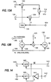
- FIGURE 13B is a preferred example of a suitable implementation of soft switch 50 which requires only one multiplier.
- the switch comprises a subtractor 1330 having an output coupled via a multiplier 1335 to one input of an adder 1340.
- the line averaged luminance signal Y8 at input 1350 is applied to the positive or non-inverting input (+) of subtractor 1330.
- the field delayed luminance signal Y9 at input 1360 is applied to adder 2340 and to the subtractive (-) input of subtractor 1330.
- the control signal K is applied to the other input of multiplier 1335.
- the field delayed luminance signal Y9 is coupled to the output 1380 via adder 1340.
- signal Y8 may be ignored because multiplier 1335 blocks the signal Y8 when K equals zero.
- multiplier 1335 couples Y8 and minus Y9 to adder 1330 which receives plus Y9 at its other input. Accordingly, for this case the Y9 signals, being our of phase, cancel each other and the adder output is signal Y8.
- the output signal comprises Y8 and Y9 blended in accordance with the control signal K. o K.
- FIG. 14 As an alternative to the use of a "soft switch” for blending the line averaged and field delayed luminance signals, one may instead use a “hard” switch as shown in FIGURE 14 controlled by a threshold detector (e.g., FIG. 10 ) This switch provides no blending but simply selects one or the other of the line-averaged (Y8) or field delayed (Y9) luminance signals depending on whether the motion signal is above or below a threshold as illustrated in FIG. 12.
- the hard switch comprises a pair of gates 1402 and 1404 having inputs 1406 and 1408 to which the line averaged (Y8) and the field delayed (Y9) luminance signals are applied and having outputs coupled to a common output terminal 1410.
- the control signal K at input 1412 is applied directly to the control input of gate 1402 and is applied via an inverter 1414 to the control input of gate 1404.
- FIGURE 15 is exemplary of one form of a motion detector suitable for use as detector 44.
- the non-delayed luminance signal Y6 and the frame delayed luminance signal Y11 are applied to respective inputs 1504 and 1506 of a subtractor and the subtractor output is applied to an absolute value circuit 1508 which provides the motion indicating signal M (at output 1510) in proportion to the absolute value of the difference of the non-delayed luminance signal Y6 and the frame delayed luminance signal Y11.
- the absolute value circuit is included in this example is that the subtractor output may be either positive or negative and only one polarity is needed for control of the blending switch 50.
- the absolute value circuit in other words, "rectifies" the subtractor output to a single polarity.
- An alternative is to omit the absolute value circuit and utilize the full subtractor output (both positive and negative values) for controlling address inputs of the control signal generator read-only memory (e.g., ROM 1102).
- Yet another alternative for motion detector 44 is the "side band energy detector" type described in the aforementioned Pritchard US Patent 4,641,186.
- the subtractor type of motion detector is preferred in the present invention because of its relative simplicity.
- FIGURES 16 and 17 illustrate alternative implementions of delay unit 42 which provides the line delayed output signal Y7, the field delayed output signal Y9 and the frame delayed output signal Y11.
- the exact delay of these signals depends, as will be readily recognized, on the video transmission standard (e.g., NTSC, PAL or SECAM).
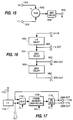
- the tapped frame delay is implemented by a cascade connection of a 1-H delay 1602, a 262 H delay 1604 and another 262H delay 1606 thereby providing delayed luminance output signals Y7, Y9 and Y11 at outputs 1603, 1605 and 1607, respectively.
- FIGURE 17 A presently preferred implementation of delay unit 42 is shown in FIGURE 17 in which the signal to be delayed is applied to the input 1702 of a 1-H delay unit 1704 and thence, via a multiplex switch 1706, to a memory 1708 that has a memory capacity of one frame and that provides a total delay of a field.
- the output of frame memory 1708 is applied to a de-multiplex switch 1710 that provides a field delayed output signal at terminal 1712 and a frame delayed output signal at terminal 1714.
- the field delayed output signal is coupled back to the other input of switch 1706 and is thereby interleaved with the frame delayed signal in the memory 1708.
- the contents of memory comprise interleaved field and frame delayed signals which are separated at the output by means of the demultiplex switch 1710. Further details of this example of tapped frame delay unit 42 are presented in US Patent US-A-4, 639,783 of R. T. Fling entitled VIDEO SIGNAL FIELD/FRAME STORAGE SYSTEM which issued January 27, 1987
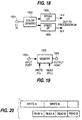
- FIGURE 18 illustrates a modification of the color signal processing in the receiver of FIGURE 1 wherein the separated chrominance signal C1 provided by separator 12 is applied to the input 1804 of a color demodulator 1804 which provides demodulated (baseband) output color signals (e.g., R-Y and B-Y) to respective speed-up units 1806 and 1808 which supply double line rate demodulated chrominance signals to the YC processor and matrix unit 24.
- Demodulation of the chrominance signal prior to speed-up does require two color speed-up circuits but is presently preferred as having the advantage of performing the demodulation at a lower clock frequency than would otherwise be required if the color demodulation were done after speed-up as in the previous example.
- FIGURE 19 is exemplary of another speed-up circuit suitable for use in the receiver of FIGURE 1 which employs a random access memory 1902 of the dual port type having an input port 1904 for receiving a digitial signal to be speeded up and an output port 1906 providing the speeded-up video output signal.
- This type of memory allows read and write operations to occur essentially at the same time which is illustrated in FIGURE 20.
- incoming lines A and B are stored in the memory in response to the write clock (CL).
- the start of the first line A read cycle starts half-way through the line A write cycle. Reading is done at twice the write clock rate and so line A is time compressed by a factor of two.
- the start of the second line A read cycle begins upon completion of the line A write cycle and at the beginning of the line B write cycle.
- the use of dual ported memories is presently preferred in that it is less complex that the other examples discussed.
- the delay involved between the start of a write cycle and the start of the first corresponding read cycle is only half of one line rather than a full line as in the previous examples.
- Various other changes may be made to the embodiment of FIGURE 1 other than those specifically enumerated and described above. For example, it is not necessary that any of the signal processing be done by the preferred method of digital signal processing. Suitable delays may be provided by other methods such as by use of CCD devices as have been described. Arithmetic operations for analog embodiments may be implemented by analog devices such as operational amplifier, resistive summing networks and the like.
- the invention, as defined by the following claims includes all analog and digital alternatives to the specific elements described.
Description
- This invention relates to television systems of a type in which interlaced video input signals are converted to a non-interlaced or "progressively scanned" form for display.
- Television systems are known in which an interlaced video signal is converted to a non-interlaced or "progressively scanned" form in which the number of horizontal lines displayed in a field is doubled. Advantageously, such systems reduce the visibility of the line structure of displayed images.
- Since doubling the number of displayed lines requires more lines than are actually transmitted, there have been a number of proposals for obtaining the required "additional" lines. An example of a system in which the required "extra" lines for display are obtained by repeating lines of a received signal is described by R. A. Dischert in U.S. patent US-A-4,415,931 entitled TELEVISION DISPLAY WITH DOUBLED HORIZONTAL LINES which issued November 15, 1983. An example of a system in which the "extra" or interstitial lines are obtained by interpolation of adjacent vertical lines of the received signal is described by K. H. Powers in U.S. patent US-A-4,400,719 entitled TELEVISION DISPLAY SYSTEM WITH REDUCED LINE-SCAN ARTIFACTS which issued August 23, 1983. Other examples include the system described by Fujimura et al. in U.S. patent US-A-4,509,071 entitled DOUBLE SCANNING NON-INTERLACE TELEVISION RECIEVER which issued April 2, 1985 and the system described by Okada et al. in U.S. patent US-A-4,451,848 entitled TELEVISION RECEIVER INCLUDING A CIRCUIT FOR DOUBLING LINE SCANNING FREQUENCY which issued May 29, 1984.
- The above mentioned systems describe arrangements in which extra lines for display are derived from a currently received field of a video input signal. This form of progressive scan conversion is commonly known as "intra-field" or "line" conversion and has an advantage in that there are no visible artifacts produced for images containing field-to-field motion. However, there is a disadvantage in that the vertical resolution of displayed images is not improved and may be degraded, particularly where vertical interpolation is employed, and this tends to "soften" displayed images.
- It has been widely recognized that the added lines needed for a progressive scan display can be obtained from a previous field rather than from a currently received field. Such systems are known generally as "field" or "inter-field" progressive scan systems and double the number of displayed lines by interleaving lines of a currently received field with lines of a previously received field. An advantage of "field" progressive scan processing is that still images are produced with the full vertical resolution of an originally scanned frame of video.
- An example of a "field progressive scan" system is described by Okada et al. in U.S. patent US-A-4,426,661 entitled TELEVISION RECIEVER INCLUDING A CIRCUIT FOR DOUBLING LINE SCANNING FREQUENCY which issued January 17, 1984. See also, U.K Application GB 2,114,848A of Achiha et al. published 24 August 1983 and entitled COLOR TELEVISION SIGNAL LINE DOUBLING CIRCUIT. Unfortunately, field progressive scan systems suffer from a problem in that if field-to-field motion exists in a scene the displayed images will be blurred.
A further problem with progressive scan processors of the type in which extra lines are derived from a previous field is that a relatively substantial amount of memory is required for storing (delaying) the lines of the previous field. - It has been recognized, however, that one may obtain a desirable reduction in the memory requirements of a field type progressive scan system by utilizing only the low frequency components of the previous field and the high frequency components of a current field in forming the extra lines for display. Such a system is described in the Japanese laid open patent application of Tanaka et al., JP-A-5879379 entitled TELEVISION RECEIVER which was laid open on May 13, 1983. Although a desirable reduction in memory requirements is achieved in the Tanaka system, the problem of motion-related artifacts remains. An additional problem is that the system disclosed requires a pair of "matched" low-pass and high-pass filters for separating the video signal. Such filters require carefully selected amplitude and phase characteristics to separate high and low video signal components without forming a gap or overlap between them and are relatively complex and expensive.
- Another example of a progressive scan processing system employing different processing of high and low frequency components is described by Dischert et al. in U.S. Pat. US-A-4,673,978 entitled PROGRESSIVE SCAN PROCESSOR WITH PLURAL FREQUENCY BAND INTERPOLATION which issued June 16, 1987. In this system the extra or "interstitial" lines for display are produced by adding a frame-combed and low pass filtered component of a video signal to a field delayed, line comb filtered and high pass filtered component of the video signal. The combined low and high frequency components are spatially and temporally coincident thereby reducing the visibility of motion artifacts (double images) during display. The system is "non-adaptive" in that the processing is not a function of scene motion.
- Systems have been proposed in which the problem of vertical resolution characteristic of line-progressive scan systems and the problem of motion blur characteristic of field progressive scan systems has been approached by making the systems "motion adaptive". In motion adaptive systems a motion detector is used to switch between the two basic types of processors as a function of motion. For example, when the incoming video signal represents a still image the signal is processed by a field type processor which generates extra lines for display by interleaving the currently received lines with lines of a previous field. Conversely, when the incoming video signal represents a moving image, the extra lines for display are obtained by interpolation (or repeating) lines of the currently received field. For images that are not still and are not in full motion it is customary to "blend" or mix the outputs of line and field type processors in proportion to the magnitude of the motion. Examples of "motion adaptive" progressive scan converters are described, for example, by Wargo et al. in U.S. patent US-A-4,716,462 entitled MOTION ADAPTIVE TELEVISION SIGNAL PROCESSING SYSTEM which issued December 29, 1987 and in U.S. patent US-A-4,598,309 entitled TELEVISION RECEIVER THAT INCLUDES A FRAME STORE USING NON-INTERLACED SCANNING FORMAT WITH MOTION COMPENSATION which issued to R. F. Casey on July 1, 1986.
- A problem characteristic of motion adaptive systems is that the memory requirements for providing motion detection are far greater than the requirements for merely providing field progressive scan processing when motion detection is implemented in the usual way by comparing video signals delayed by one full frame. One approach to avoiding the requirement for a full frame of memory is to detect motion by measurement of the video signal sideband energy. An example of such a system is described by D. H. Pritchard in US patent 4,641,186 entitled MOTION DETECTOR THAT EXTRACTS MOTION INFORMATION FROM SIDEBANDS OF A BASEBAND TELEVISION SIGNAL which issued February 1987. Although a full frame of memory is avoided, the sideband energy motion detection method is, however, relatively complicated.
- The present invention resides in part in the recognition of the need for a progressive scan system which effectively avoids the foregoing problems while retaining the advantages of each of the earlier solutions. The invention provides an apparatus as claimed in
claim 1. - Progressive scan conversion apparatus, embodying the invention includes a source for providing a video input signal of a given line rate. A processor, coupled to the source, provides a video difference signal representative of a difference between a first low frequency component derived from a current line of said video input signal and a second low frequency component derived from at least one previous line of the video input signal. An output circuit time compresses and combines the video difference and input signals and forms a progressive scan output signal.
- In an exemplary embodiment of the invention, the output circuit includes circuit means for doubling the line rate of the video difference signal, for doubling the line rate of the video input signal and for adding a line of the double line-rate video difference signal to every other line of the double line-rate video input signal for forming said progressive scan output signal.
- In presently preferred embodiment of the invention, the video input signal is of digital form, the processor includes means for sub-sampling the video input signal prior to forming the video difference signal and the output circuit includes means for up-sampling the video difference signal prior to the addition of the double line-rate video signals to form the progressive scan output signal.
- The foregoing and further features of the invention are described hereinafter and are illustrated in the accompanying drawing wherein like elements are denoted by like reference designators and in which:
- FIGURE 1 is a block diagram of a television receiver embodying the invention;
- FIGURE 2 is a block diagram illustrating a modification of a portion of the receiver of FIGURE 1;
- FIGURE 3 is a block diagram illustrating another modification of a portion of the receiver of FIGURE 1;
- FIGURE 4 is a block diagram of a "speed-up" circuit suitable for use in the receiver of FIGURE 1;
- FIGURE 5 is a block diagram of an alternative "speed-up" circuit suitable for use in the receiver of FIGURE 1;
- FIGURE 6 is a block diagram of a sub-sampling circuit suitable for use in the receiver of FIGURE 1;
- FIGURE 7 is a block diagram of an averaging circuit suitable for use in the receiver of FIGURE 1;
- FIGURES 8A and 8B are block diagrams of a sample rate converters of the interpolation type suitable for use in the receiver of FIGURE 1;
- FIGURE 9 is a pixel diagram of the sample rate converters of FIGURES 8A and 8B;
- FIGURES 10 and 11 are block diagrams of control signal generators suitable for use in the receiver of FIGURE 1;
- FIGURE 12 is a response diagram illustrating various transfer functions of the control signal generators of FIGURES 10 and 11;
- FIGURES 13A and 13B are block diagrams of "soft switchs" suitable for use in the receiver of FIGURE 1;
- FIGURE 14 is a block diagram of a "hard switch" suitable for use in the receiver of FIGURE 1 as an alternative to the "soft switch" of FIGURE 13;
- FIGURE 15 is a block diagram of a motion detector suitable for use in the receiver of FIGURE 1;
- FIGURES 16 and 17 are block diagrams of frame delay circuits having line and field taps and which are suitable for use in the receiver of FIGURE 1;
- FIGURE 18 is a block diagram illustrating a modification of the color signal processing in the receiver of FIGURE 1;
- FIGURE 19 is a further example of a speed-up circuit suitable for use in the receiver of FIGURE 1; and
- FIGURE 20 is a read/write timing diagram illustrating the operation of the speed-up circuit of FIGURE 19.
- The television receiver 10 of FIGURE 1 includes a progressive scan processor 30 (outlined in phantom) comprising an
input unit 30A (outlined in phantom) and anoutput unit 30B (outlined in phantom). As an over-view of certain salient features of the invention, theinput unit 30A provides a video difference signal (Y12) representative of a difference between a first low frequency component (Y6) derived from a current line of a video input signal (Y3) and a second low frequency component (Y10) derived from at least one previous line of the video input signal (Y3). Theoutput unit 30B processes the video difference signal (Y12) and the video input signal (Y3), as will be explained, to form a progressive scan luminance output signal (Y2) of double the line rate of the input signal. - Advantageously, the combination of the input (30A) and output (30B) units of the progressive scan processor (30A,30B) provide a progressive scan output signal (Y2) having the relatively high vertical resolution characteristic of field progressive scan systems; having the motion artifact immunity characteristic of line progressive scan systems; having the motion adaptability characteristic of motion adaptive systems; and having substantially reduced system memory requirements as compared with conventional motion adaptive systems. Additionally, the system provides "dual band" video processing without requiring the use of conventional complementary high pass and low pass filters for band splitting.
- In more detail, the receiver 10 of FIGURE 1 comprises a luminance-chrominance
signal separation circuit 12 which separates a composite video input signal S1 into a luminance component Y1 and a chrominance component C1. The input video signal S1 may be provided by a conventional tuner, IF amplifier anddetector unit 14 from an antenna orcable input 16 or, alternatively, it may be provided by anauxiliary input terminal 18 or some other suitable source.Separation circuit 12 may be of conventional design such as a comb filter or a combination of high and low pass filters as is well known. - The separated chrominance signal component C1 is applied to a speed-up
unit 20 which time compresses and repeats each line thereof to provide a chrominance output signal C2 having double the line rate of the video input signal and in which each line is repeated. Examples of suitable "speed-up" circuits are described later. - The luminance signal Y1 is converted to digital form by means of an analog-to-digital (A/D)
converter 13 and the digitized luminance signal Y3 is applied to a luminance signal progressive scan processor 30 (outlined in phantom) which generates a motion adaptive double line-rate progressively scanned luminance output signal Y2 as will be described. This signal is converted back to analog form (Y5) by means of a digital to analog (D/A)converter 23 and the double line-rate signals C2 and Y5 are applied to a conventional luminance-chrominancesignal processing unit 24 which provides such functions as color demodulation, brightness and contrast control and color matrixing so as to provide a progressively scanned output signal S2 of a form (e.g., RGB component form) suitable for display by akinescope 26 or some other suitable display device (e.g., an LCD device or a projection display). - Since the line rate of the output signal S2 is twice that of the input signal S1, the images produced by
kinescope 26 have twice as many lines as the input signal whereby the visibility of raster line structure is substantially reduced as compared with conventional interlaced images. - Clock signals CL for
converters 13 and 23 (and other timing signals for the receiver 10) are provided by atiming signal generator 21. This generator may comprise a phase locked loop (PLL) generator of conventional design locked to a multiple of the color burst component of the input signal S1 or locked to a multiple of the line frequency of the input signal S1. Typical sampling clock frequencies are three or four times the frequency of the color subcarrier for systems employing what is commonly called "burst locked" clocking. In a presently preferred implementation of the system thetiming signal generator 21 is phase locked to a multiple of the horizontal line rate. This is commonly called "line locked" clock generation and has an advantage over burst locking in that the system is usable with so-called non-standard video sources where the relationship between line and burst frequencies may vary. Illustratively, in this specific example of the invention, the clock frequency CL is selected to be 1024 times the horizontal line rate of the video input signal. For NTSC standard sources, this frequency CL is about 16.1 mega-Hz. Other clock signals provided by timingunit 21 include CL/4 and 2CL which are used for sample rate conversions as will be explained.Unit 21 also provides horizontal and vertical line rate frequencies used for deflection purposes. - The remaining portion of FIGURE 1 comprises the
progressive scan processor 30 that provides the motion adaptively processed progressively scanned luminance output signal Y2. It will be noted that the motion adaptive components of Y2 are derived by processing only sub-sampled low frequency components of the luminance signal Y3. Advantageously, restricting the processing in this manner greatly reduces the amount of memory required for implementing line, field and frame delays necessary for motion adaptive processing as compared with processing of full bandwidth signals. - A further advantage, as will be explained, relates to the use of "differential" processing (i.e., processing of signal differences rather than absolute values). Differential processing, as used in the present invention, eliminates the need for special high pass and low pass filters having matched amplitude and phase response characteristics that are required in conventional split-band processing systems as previously described. Such high pass and low pass filters having truly complementary amplitude and phase characteristics are complex and expensive.
- In more detail, for purposes of illustration and explanation of this embodiment of the invention, the
progressive scan processor 30 is divided, by phantom lines, into two portions comprising aninput circuit 30A and anoutput circuit 30B. - In
input circuit 30A ofprogressive scan processor 30 the full bandwidth luminance signal Y3 is applied to asub-sampling circuit 40 by means of alow pass filter 37.Sub-sampling unit 40 is clocked at a rate of CL/4 and greatly reduces the luminance signal data rate and thus reduces the number of bytes of memory required for implementing video delay functions. As an example, if the full bandwidth luminance signal is digitized at a the assumed clock rate of (about) 16 MHz and then sub-sampled at a 4 MHz clock rate then only one-quarter of the memory will be needed to implement the same digital delay as would be required if the signal were not sub-sampled. One may, if desired, select other clock rates and sub-sampling rates in a specific application of the principles of the invention. - To avoid aliasing, the sub-sampled signal is low pass filtered prior to sub-sampling and this function is provided by
low pass filter 37. A suitable cut-off frequency forfilter 37 is about one-half of the sub-sampling rate (e.g., about 2 MHz for the assumed sub-sampling rate of about 4 MHz.) In practice, it is desirable that the filter cut-off frequency be slightly lower than half the sub-sampling rate to allow for the finite slope of the filter response in the transition region between the filter pass band and the filter stop band. An exemplary cut-off frequency, for the assumed sampling frequency. is about 1.5 MHz for 6 dB of attenuation at band edge. This frequency is well below the Nyquist rate of 2.0 MHz for the assumed sampling rate of about 4 MHz. Advantageously, this reduces the number of filter elements needed to implement the anti-aliasinglow pass filter 37. For applications where the sub-sampling rate is higher, then proportionally higher anti-aliasing filter cut-off frequencies may be used. - The sub-sampled and low-pass filtered luminance signal Y6 is applied to the inputs of a tapped
frame delay unit 42, amotion detector 44, anaverager 45 and asubtractor 48.Delay unit 42 has output taps providing a one-line (1-H) delayed luminance signal Y7, a one field delayed (263 H) delayed luminance signal Y9 and a frame (525H) delayed luminance signal Y11. For PAL standard systems the field delay would be 313 lines and the frame delay would be 625 lines. The one line (1-H) delayed output tap ofdelay unit 42 is connected to the other input ofaverager 46 which provides a line averaged output signal Y8. - A "soft switch" 50 combines the averaged luminance signal Y8 with a field delayed luminance signal Y9 to provide a combined or "blended" luminance output signal Y10 in which the proportions of the Y8 and Y9 components are controlled by
motion detector 44 and acontrol signal generator 46. An example of a suitable soft switch is shown and described later.Motion detector 44 has one input connected to receive the non-delayed luminance signal Y6. It has a second input connected to receive a frame delayed luminance signal Y11 provided bydelay unit 42 and provides a motion indicating signal M representative of the difference between signals Y6 and Y11. A suitable motion detector is shown and described later. The purpose ofcontrol signal generator 46 is to convert the motion signal M, which is linearly related to motion, to a control signal K which is non-linearly related to motion so as to provide a better match to the motion sensitivity of the human visual system. Examples of suitable control signal generators are shown and described later. -
Soft switch 50 responds to the control signal K by selecting the field delayed luminance signal Y9 under conditions of little or no motion (K=0) and selecting the line averaged luminance signal Y8 under conditions of high motion (K=1). For intermediate values of motion the signals Y8 and Y9 are blended in proportion to the non-linear control signal K provided bycontrol signal generator 46. - The resultant "motion adapted" luminance signal Y10 provided by
soft switch 50 is applied to the second input ofsubtractor 48 which receives the non-delayed, sub-sampled and low-pass filtered luminance signal Y6 at its other input and provides a luminance output difference signal Y12. The signal Y12 is a video difference signal representative of a difference between a first low frequency component (Y6) derived from a current line of the video input signal and a second low frequency component (Y10) derived from at least one previous line of the video input signal. - The
output circuit 30B ofprogressive scan processor 30 selectively combines the video difference signal (Y12) with the full bandwidth video input signal Y3 to form the progressive scan video output signal Y2. Inoutput circuit 30B the full bandwidth luminance signal Y3 is applied to a speed-upunit 36 which time compresses and repeats each line thereof to provide a double line-rate luminance output signal Y4 in which each line is time compressed by a factor of two and repeated. The difference signal Y12 produced bysubtractor 48 is applied to a luminance signal speed-upunit 54 that time compresses each line thereby doubling the line rate of the difference signal Y12. Doubling the line rate of the sub-sampled signal Y12 also doubles the sample rate (e.g., from 4 to 8 MHz for the assumed clock) of the speeded up signal Y13. The sample rate of signal Y13 is then applied to a sample rate converter ("UP SAMPLE") 56 that quadruples the sample rate of the time compressed signal Y13. This sample rate conversion may be implemented by repeating samples or by interpolating samples. Accordingly, for the assumed clock and sub-sampling values, the processed low frequency difference signal Y14 at the output of "up-sample"converter 56 equals about 32 MHz which equals the sample rate of the speeded-up broad band luminance signal Y4. - The sample rate equalization or "matching" of the processed luminance signal lows (Y14) and the full bandwidth luminance signal (Y4) allows the direct addition of these signals in
adder 38 to form the luminance progressive scan signal Y2. The last step, prior to the addition, is to apply signal Y14 to aswitch 57 which is synchronized with the line frequency so as to modify every other line of the processed signal Y4 to produce the progressive scan output signal Y2. - In the embodiment of FIGURE 1 described thus far there has been shown and described a
progressive scan processor 30 having a number of features which include: (1) motion artifacts are minimized by motion adaptive processing provided byswitch 50 which selects line averaged or field delayed signals as a function of motion; (2) memory requirements are substantially reduced by processing sub-sampled low frequency luminance components taken from the present line and a selected previous line; and (3) the processed output signal is formed by combining processed low frequency difference components with the full bandwidth luminance signal. This latter feature completely eliminates the need for complementary high pass and low pass filters having matched amplitude and phase responses as would otherwise be required if the luminance signal band were to be "split" or divided into high-pass and low-pass components for processing of the signal. - The foregoing description presents the general operation of
processor 30 in FIGURE 1. The overall operation is relatively complex because it depends on picture content but may be easily understood by considering a few specific examples. As a first example, assume that the video image being processed is a still picture. For this case there is no frame-to-frame difference in pixels (picture elements) and so the output M ofmotion detector 44 will be zero indicating no motion. Control signal K provided bygenerator 46 is a non-linear function of M as previously noted. For purposes of illustration it will be assumed that K equals zero for the case where M equals zero.Soft switch 50 will respond to the zero value of control signal K by selecting the field delayed output signal Y9 offrame delay unit 42.Subtractor 48 will thus subtract the field delayed low frequency component Y9 from the current low frequency component Y6 to provide the difference signal Y12.Adder 38 will then add one line of the speeded up and sample rate converted difference signal Y14 (selected by switch 57) to every other line of the speeded up full bandwidth luminance signal Y4 to form the progressive scanned luminance output signal Y2. - As a result of the addition in
adder 38, the luminance signal will comprise two components in different frequency bands even though the system employs no high pass filters. A first component, taken from a currently received line, will equal a high frequency component of the full bandwidth signal Y3 for frequencies above the cut-off frequency oflow pass filter 37. A second component will equal a low frequency component, selected byfilter 37, taken from the previous field. This may be understood by considering that the difference signal Y12 actually comprises two low frequency components (Y6 and Y10) and the phase of a selected one of these components (Y6) is reversed due to the subtraction. Accordingly, ignoring for the moment the speed-up and sample rate conversions, the output signal Y2 equals the full bandwidth luminance signal Y3, minus the low frequency component of Y3 passed byfilter 37, plus the low frequency component of Y3 passed byfilter 37 but taken from the previous field. When these signals are combined the low frequency components of the current line of signal Y3 simply cancel out because they are out of phase. The missing lows due to the cancellation are replaced by the lows from the previous field (Y10). Since high frequency components of signal Y3 are not processed inprocessor 30A these components of Y3 are not disturbed and form the high frequency component of the output signal Y2. - Briefly summarized, for the still image example, alternate lines of the output signal Y2 comprise the full bandwidth luminance signal Y3 and the in-between or "interstitial" lines comprise a high frequency component (above the cut-off frequency of filter 37) taken from the currently received line (Y3) and a low frequency component (9) taken from the previous field. Accordingly, for this example low frequency video components that are displayed will exhibit the full vertical resolution of a complete video frame. Visually, the effect is to increase the vertical resolution of displayed still images as compared with standard interlaced images.
- As a further example of overall operation of the FIGURE 1 system, consider the case in which there is substantial motion in a scene. In this case the
soft switch 50 selects only the line averaged low frequency luminance signal Y8 so that the low frequency difference signal Y12 equals the difference between the low frequency component Y6 of a current line and the average Y8 of the low frequency components of the current and a previous line. When these signals are speeded up and converted to the same sample rates inoutput circuit 30B the resultant sum signal (for every other line) comprises a low frequency component equal to the average of the current and previous lines and a high frequency component taken from the current line. For the remaining lines the output equals the current line. - For the case where motion exists between full motion (M=1) and no motion (M=0)
switch 50 blends the line averaged signal Y8 and the field delayed signal Y9 to form the signal Y10 which after subtraction of signal Y6 forms the difference signal Y12. As a result, the output signal Y2 includes a high frequency component derived from the currently received line and a low frequency component derived (by motion dependent blending in switch 50) from two lines of the current field or one line of a previous field depending on the degree of the image motion. - In the foregoing discussion of processing of still images in FIGURE 1 it was noted that the difference signal Y12 was formed by subtracting Y6 from Y10 and that this resulted in a reversal of the phase of the current low frequency component Y6 relative to the phase of the full bandwidth signal Y6 to thereby cancel these components when they are later combined by addition in
adder 38. As an alternative, the signal Y10 may be subtracted from Y6 to form the difference signal Y12 along with modifying theoutput circuit 30B as will now be described. - FIGURE 2 illustrates a modification of the
progressive scan processor 30 of FIGURE 1 wherein the inputs tosubtractor 48 are reversed ininput circuit 30A and inoutput circuit 30B theadder 38 is replaced by a subractor 39 that subtracts every other line of signal Y14 from the full bandwidth luminance signal Y4. This embodiment of the invention is functionally identical to that of FIGURE 1 and is structurally identical except for the two noted changes. - In more detail, in the FIGURE 1 embodiment signal Y6 was subtracted from signal Y10 to form the low frequency difference signal Y12. The addition of signals Y12 and Y3 (after speedup and sample rate equalization) resulted in an output signal Y2 having high frequency components taken from the current line and low frequency components derived from the previous line or field. In FIGURE 2 the same result is obtained when the inputs of
subtractor 48 ininput circuit 30A are reversed by replacing theadder 38 inoutput circuit 30B with a subtractor 39. The functional result is the same because in this example the signal "blended" low frequency luminance signal Y10 is doubly inverted bysubtractors 48 and 39 and so is effectively added to the signal Y3 whereas the low frequency luminance signal Y6 is inverted only once (in subtractor 39) and is thus effectively subtracted from signal Y4. This is exactly the same result as is achieved in the example of FIGURE 1. - In view of the foregoing, it does not make a functional difference if one subtracts Y6 from Y10 and later adds signals Y14 and Y4 (as in FIGURE 1) or if one subtracts signal Y10 from Y6 and later subtracts signal Y14 from Y4 as in FIGURE 3. However, the example of FIGURE 1 is presently preferred because it requires only one subtractor (rather than two) and thus requires less hardware for implementation since addition is less complicated in digital processing than subtraction. In addition to the apparent economic benefit of using fewer parts, the example of FIGURE 1 has the technical advantage as well of providing higher reliability as there are fewer parts to fail.
- FIGURE 3 illustrates a modification of the
output circuit 30A ofprogressive scan processor 30 wherein the positions of the sample rate converter ("up-sample")circuit 54 and the speed-up circuit 56 are reversed in the cascade connection of these two circuit elements. To effect this change all that is required is an appropriate selection of the various clock frequencies. The speed-up circuit, for example requires a read clock that is twice the write clock frequency and the sample rate conversion requires a read clock that is four times the write clock frequency. In the example of FIGURE 1 where speed-up is done before sample rate conversion the speed-up circuit receives a write clock frequency of CL/4 (e.g., 4 MHz) and a read clock frequency of CL/2 (e.g., 8 MHz) and the sample rate converter receives a write clock frequency of CL/2 (e.g., 8 MHz) and a read clock frequency of 2CL (e.g., 32 MHz). In the example of FIGURE 3, where sample rate conversion is done before speed-up the clock frequencies are changed as follows: (1) the write and read clocks for speed-up are changed to CL and 2CL, respectively, (e.g., 16 and 32 MHz) and (2) the write and read clocks for sample rate conversion are changed to CL/4 and CL, respectively (e.g., about 4 and 16 MHz). The overall operation of the speed-up and sample rate converters provides exactly the same result as in the example of FIGURE 1 in that the sub-sampled difference signal Y12, after sample rate conversion and speed-up, is of the same line rate and sample rate as the speeded up full bandwidth luminance signal Y3 and so these signals may be combined (by addition as in FIG. 1 or by subtraction as in FIG. 2) to provide the progressively scanned output signal Y2. - FIGURES 4 and 5 are exemplary of "speed-up" circuits suitable for doubling the line rate of chrominance or luminance input signals in the receiver of FIGURE 1. In FIGURE 4 video signals to be "speeded-up" at
input 402 are alternately applied via a line rate operated "write"switch 404 to a pair of one line (1H)CCD memories output 412 via aread switch 410. Since the read clock rate is twice the write clock rate the input signal is thereby time compressed and repeated and so the output signal is of double the input signal line rate with each line being repeated. Since CCD memories require refreshing to be read twice, each of thememories switch signal separation filter 12 provides a chrominance output signal of analog form. Advantageously, this form of speedup circuit accepts analog signals directly without need for analog to digital conversion. Another alternative (for digital input signals) is to use a dual port memory (as discussed later) which is less complex that separately switched one-line memories. - The speed-up circuit of FIGURE 5 is similar to that of FIGURE 4 but employs digital (binary) memories as storage devices rather than CCD type storage devices. Operation is otherwise the same as in the example of FIGURE 4 with the exception that refresh circuits are not required for the digital memory. This type of speed-up circuit may be used directly for the luminance signal processing in
processor 30 because the signals there are already of binary form. To use this speed-up circuit for the chrominance signal C1 in the example of FIG. 1, it would be necessary to add an analog-to-digital converter to the input ofswitch 504 and to add a digital to analog converter to the output (512) ofswitch 510. This would not be necessary, of course if thesignal separation circuit 12 is a digital type of circuit providing output signals that are already of digital form rather than analog form. If the example of FIGURE 1 is modified to provide digital signal separation, then analog todigital converter 13 may be eliminated. - FIGURE 6 is exemplary of a sub-sampling circuit suitable for use as
circuit 40 inprocessor 30A. The circuit comprises alatch 602 having adata input 604 which receives the low pass filtered luminance signal Y3, having aclock input 605 to which the sub-sampling clock signal is applied and having anoutput 606 providing the sub-sampled output signal Y6. The data latch may be clocked at a rate CL/N where N is a number greater than unity. Preferably, N is an integer such as 2, 3 or 4. As an alternative, N may be an non-integer fraction. The advantage of using integer values for N (which is preferred) is that no interpolation is required to produce the sub-sampled signal. However, non-integer values of N may be employed in a particular system if desired. The presently preferred integer sub-sampling values are 2, 3 and 4. - In the specific embodiment shown herein, for purposes of illustration of the invention, the value of N is chosen to be N=4. For the four-to-one sub-sampling assumed in the example of FIGURE 1 which uses a clock frequency of CL/4, the
latch 602 would discard three out of four samples of the low pass filtered luminance signal Y3. Accordingly, for this sub-sampling value (N=4) the memories required for implementing video delay need be only one-quarter as large as would be required if the video signal were not sub-sampled. -
Averager 46 may be implemented as shown in FIGURE 7 by applying the non-delayed and 1-H delayed signals to the inputs (704,706) of anadder 702 and dividing the adder output by two with adivider 708 to thereby provide a line averaged output signal Y8 atoutput terminal 710. In practice, the divider may be implemented by simply not using the LSB output of the adder and thus providing a one bit shift of the adder outputs. For systems in which the signal processing at this point is done in analog form the divider would be replaced by a 6 dB attenuator and the adder would be replaced by a summing network. - FIGURE 8A is an example of a sample rate converter of the "interpolating type" which may be used for quadrupling the sample rate of the luminance difference signal. As previously explained, one may provide sample rate up-conversion by simply repeating each sub-sampled pixel four times. Sample rate up-conversion by repeating samples, however, tends to produce images with relative coarse diagonal line structure. Interpolating converters, such as in FIGURE 8A (and FIG. 8B discussed later), exhibit smoother diagonal lines but somewhat "softer" horizontal transitions.
- In more detail,
converter 56 in FIGURE 8A includes asample delay unit 802 having aninput 804 to which the sub-sampled luminance signal Y13 is applied.Delay unit 802 also receives a clock signal CL/2 which equals the sample rate of signal Y13 and so imparts a one sample delay to signal Y13. The input (A) and output (B) signals ofdelay unit 802 are applied to the inputs of three arithmetic units 806,808, and 810 which generate respective output signals of (3A+B)/4, (A+B)/2 and (A+3B)/4. The output signals ofarithmetic units delay unit 802 are applied to a multiplex (MUX)switch 812 which sequentially selects the signals at a clock rate of 2CL. This clock rate is four times the clock rate applied to sampledelay unit 802 and so the interpolated and multiplexed signals provided byswitch 812 tooutput terminal 814 have four times the sample rate as the input signal Y13. - FIGURE 9 is a pixel diagram illustrating the operation of the sample rate converter of FIGURE 8A (and FIG. 8B, discussed later) for the case where the currently received pixel A is at black level (e.g., zero IRE units) and the previous pixel B was at white level (e.g., 100 IRE units). As shown,
multiplex switch 812 sequentially selects the arithmetic unit outputs to provide interpolated pixels having luminance levels of (A+3B)/4, (A+B)/2 and (3A+B)/4 which lie between the values of the current (A) and previous (B) pixels. Accordingly, a linear approximation of pixel values is produced at four times the input sample rate. As previously noted, the use of interpolation has an advantage in producing smoother diagonal lines that the alternative sample rate conversion method of simply repeating each incoming pixel to quadruple the sample rate. - FIGURE 8B is a block diagram of (preferred) alternative form of an interpolating sample rate converter which does not require the use of multipliers as in the arrangement of FIGURE 8A. The converter comprises an
input terminal 820 to which luminance signal Y13 is applied and anoutput terminal 830 at which the 1:4 sample rate interpolated luminance signal Y14 is produced.Terminal 820 is coupled toterminal 830 via a cascade connection comprising a 1 to 4sample rate repeater 822, digital filter having a Z-transform of 1-Z (exp. -1), a second digital filter having a Z transform of 1-Z (exp. -2) 826 and a divide by fourdivider 828. Thesample repeater 822 repeats incoming samples to provide four identical output samples for each sample received. The first digital filter may be implemented as an adder which adds an input sample to a previous sample delayed by one sample interval. No multiplication is required. The second digital filter may be implemented by an adder which adds the output of the first filter to a signal corresponding to the output of the first filter delayed by two sample periods. Again, no multiplication is required. The output of the second filter is scaled down by a factor of four bydivider 828. The output signal thus produced is the same as in the previous example. Advantageously, in this preferred embodiment of the sample rate converter, no multiplication is required at any stage and so the circuit is substantially simplified over that of the previous example. - FIGURES 10, 11 and 12 illustrate various alternative implementations and alternative non-linear response characteristics for
control signal generator 46. In its most simple form thecontrol signal generator 46 may be implemented, as shown in FIGURE 10, by applying the motion indicating signal M to oneinput 1004 of athreshold detector 1002 which receives a reference signal R at itsother input 1006 and provides a binary valued (i.e., on/off) output signal atoutput 1008 indicating when the motion indicating signal M is above or below the reference signal. This, threshold type of operation is illustrated by response curve K-1 in FIGURE 12 where it is seen that for values of the motion signal M below the reference level R the value of the control signal K is zero, otherwise, the value of the control signal K is unity. - FIGURE 11 illustrates a preferred implementation of the
control signal generator 46 in which the motion indicating signal M is applied to the address inputs 1104 of a read-only memory (ROM) 1102 which provides the control signal K at itsoutput 1106. This generator can produce the threshold response of curve K-1 shown in FIGURE 12 and it can also produce other, more complex, non-linear responses illustrated by the response curves K-2 and K-3 in FIGURE 12. In the example of response K-2 in FIGURE 12 the control signal K changes relatively slowly for small and large values of the motion signal M and changes relatively rapidly for intermediate values of the motion signal M. In the example of response K-3 the control signal increases rapidly for small values of motion and increases less rapidly for larger values of motion. The use of non-linear response curves forcontrol signal generator 46 is preferred over the example of binary valued threshold detection because changes in the curves (e.g., K-2 or K-3) are much less abrupt and thus less noticeable to a viewer of the processed video signal. - FIGURE 13A is an example of a suitable implementation of
soft switch 50 which comprises a pair ofmultipliers inputs adder 1310 that provides the blended luminance signal Y10 at itsoutput 1312.Multiplier 1304 is controlled directly by the control signal K applied to input 1314 andmultiplier 1302 is controlled by a signal equal to 1-K provided by a read only memory (ROM) 1316 which is addressed by the control signal K. - In operation, for no motion (K=0)
multiplier 1302 passes the field delayed luma signal Y9 to the output viaadder 1310 andmultiplier 1304 blocks the line averaged luminance signal Y8. For high motion (K=1) the line averaged luminance signal Y8 is passed to the output bymultiplier 1304 andadder 1310 and the field delayed luminance signal is blocked bymultiplier 1302. For intermediate degrees of motion (0<K<1) the output signal is blended or combined in the proportions of K and 1-K. - FIGURE 13B is a preferred example of a suitable implementation of
soft switch 50 which requires only one multiplier. The switch comprises asubtractor 1330 having an output coupled via amultiplier 1335 to one input of anadder 1340. The line averaged luminance signal Y8 atinput 1350 is applied to the positive or non-inverting input (+) ofsubtractor 1330. The field delayed luminance signal Y9 atinput 1360 is applied to adder 2340 and to the subtractive (-) input ofsubtractor 1330. The control signal K is applied to the other input ofmultiplier 1335. - In operation, when there is no motion (K=0) the field delayed luminance signal Y9 is coupled to the
output 1380 viaadder 1340. For this case signal Y8 may be ignored becausemultiplier 1335 blocks the signal Y8 when K equals zero. For the case where there is a lot of motion (K=1)multiplier 1335 couples Y8 and minus Y9 to adder 1330 which receives plus Y9 at its other input. Accordingly, for this case the Y9 signals, being our of phase, cancel each other and the adder output is signal Y8. For any value of K between the limits one and zero (0<K<1) the output signal comprises Y8 and Y9 blended in accordance with the control signal K. o K. - As an alternative to the use of a "soft switch" for blending the line averaged and field delayed luminance signals, one may instead use a "hard" switch as shown in FIGURE 14 controlled by a threshold detector (e.g., FIG. 10 ) This switch provides no blending but simply selects one or the other of the line-averaged (Y8) or field delayed (Y9) luminance signals depending on whether the motion signal is above or below a threshold as illustrated in FIG. 12. The hard switch comprises a pair of
gates inputs common output terminal 1410. The control signal K atinput 1412 is applied directly to the control input ofgate 1402 and is applied via aninverter 1414 to the control input ofgate 1404. - In operation, if the motion signal M is greater than the reference voltage R then K will equal unity and
gate 1402 will be enabled thereby coupling the line averaged luminance signal Y8 to theoutput 1410. Otherwise,gate 1404 is enabled so as to couple the field delayed luminance signal Y9 to theoutput 1410. This form of "hard" switching has an advantage in terms of simplicity over the preferred alternative of "soft" switching which, as previously noted, has an advantage in providing smoother transitions between line and field processing for scenes having substantial changes in motion - FIGURE 15 is exemplary of one form of a motion detector suitable for use as
detector 44. In this example the non-delayed luminance signal Y6 and the frame delayed luminance signal Y11 are applied torespective inputs absolute value circuit 1508 which provides the motion indicating signal M (at output 1510) in proportion to the absolute value of the difference of the non-delayed luminance signal Y6 and the frame delayed luminance signal Y11. The reason the absolute value circuit is included in this example is that the subtractor output may be either positive or negative and only one polarity is needed for control of the blendingswitch 50. The absolute value circuit, in other words, "rectifies" the subtractor output to a single polarity. An alternative is to omit the absolute value circuit and utilize the full subtractor output (both positive and negative values) for controlling address inputs of the control signal generator read-only memory (e.g., ROM 1102). Yet another alternative formotion detector 44 is the "side band energy detector" type described in the aforementioned Pritchard US Patent 4,641,186. The subtractor type of motion detector is preferred in the present invention because of its relative simplicity. - FIGURES 16 and 17 illustrate alternative implementions of
delay unit 42 which provides the line delayed output signal Y7, the field delayed output signal Y9 and the frame delayed output signal Y11. The exact delay of these signals depends, as will be readily recognized, on the video transmission standard (e.g., NTSC, PAL or SECAM). In the example of FIGURE 16 (where NTSC standard is assumed) the tapped frame delay is implemented by a cascade connection of a 1-H delay 1602, a 262H delay 1604 and another262H delay 1606 thereby providing delayed luminance output signals Y7, Y9 and Y11 atoutputs - A presently preferred implementation of
delay unit 42 is shown in FIGURE 17 in which the signal to be delayed is applied to theinput 1702 of a 1-H delay unit 1704 and thence, via amultiplex switch 1706, to amemory 1708 that has a memory capacity of one frame and that provides a total delay of a field. The output offrame memory 1708 is applied to ade-multiplex switch 1710 that provides a field delayed output signal at terminal 1712 and a frame delayed output signal at terminal 1714. The field delayed output signal is coupled back to the other input ofswitch 1706 and is thereby interleaved with the frame delayed signal in thememory 1708. By this means, the contents of memory comprise interleaved field and frame delayed signals which are separated at the output by means of thedemultiplex switch 1710. Further details of this example of tappedframe delay unit 42 are presented in US Patent US-A-4, 639,783 of R. T. Fling entitled VIDEO SIGNAL FIELD/FRAME STORAGE SYSTEM which issued January 27, 1987. - FIGURE 18 illustrates a modification of the color signal processing in the receiver of FIGURE 1 wherein the separated chrominance signal C1 provided by
separator 12 is applied to theinput 1804 of acolor demodulator 1804 which provides demodulated (baseband) output color signals (e.g., R-Y and B-Y) to respective speed-upunits 1806 and 1808 which supply double line rate demodulated chrominance signals to the YC processor andmatrix unit 24. Demodulation of the chrominance signal prior to speed-up, as shown in this example, does require two color speed-up circuits but is presently preferred as having the advantage of performing the demodulation at a lower clock frequency than would otherwise be required if the color demodulation were done after speed-up as in the previous example. - FIGURE 19 is exemplary of another speed-up circuit suitable for use in the receiver of FIGURE 1 which employs a
random access memory 1902 of the dual port type having aninput port 1904 for receiving a digitial signal to be speeded up and anoutput port 1906 providing the speeded-up video output signal. This type of memory allows read and write operations to occur essentially at the same time which is illustrated in FIGURE 20. As shown incoming lines A and B are stored in the memory in response to the write clock (CL). The start of the first line A read cycle starts half-way through the line A write cycle. Reading is done at twice the write clock rate and so line A is time compressed by a factor of two. The start of the second line A read cycle begins upon completion of the line A write cycle and at the beginning of the line B write cycle. The use of dual ported memories is presently preferred in that it is less complex that the other examples discussed. It will also be noted that the delay involved between the start of a write cycle and the start of the first corresponding read cycle is only half of one line rather than a full line as in the previous examples. Various other changes may be made to the embodiment of FIGURE 1 other than those specifically enumerated and described above. For example, it is not necessary that any of the signal processing be done by the preferred method of digital signal processing. Suitable delays may be provided by other methods such as by use of CCD devices as have been described. Arithmetic operations for analog embodiments may be implemented by analog devices such as operational amplifier, resistive summing networks and the like. The invention, as defined by the following claims includes all analog and digital alternatives to the specific elements described.
Claims (4)
- Progressive scan conversion apparatus, comprising:
a source (13) for providing a digital video input signal (Y3) of an interlaced format, and of a given line rate and a given sample rate;
characterized by:a sub-sampling circuit (40) coupled to said source (13) for providing a sub-sampled video signal (Y6);a motion adaptive processor (42-50) responsive to said sub-sampled video signal for providing as the processor output an average of a pair of adjacent lines of said sub-sampled video signal under conditions of little or no motion, for providing as the processor output a field-delayed version of said sub-sampled video signal under conditions of high motion, and for providing as the processor output a combination of said adjacent lines average and said field delayed version under conditions of intermediate values of motion;a subtractor (48) having inputs coupled to receive said sub-sampled video signal (Y6) and the output (Y10) of said motion adaptive processor (42-50) and having an output for providing a sub-sampled video difference signal (Y12);first means (36) for doubling the line rate of said video input signal (Y3);second means (54,56) for doubling the line rate and for increasing the sample rate of said sub-sampled video difference signal (Y12) to provide a processed video difference signal (Y14) having the same line rate and sample rate as a double line-rate video signal (Y4) produced by said first means;a switch (57) for selectively passing alternate lines of said processed video difference signal; andcombiner means (38), responsive to the outputs of said first means and said switch, for providing a progressive scan output signal (Y2). - Apparatus as recited in Claim 1, characterized in that said combiner means comprises: adder means (38) for adding output signals provided by said switch (57) to said double line rate video input signal (Y4) to form said progressive scan output signal (Y2).
- Apparatus as recited in Claim 1, characterized in that said combiner means comprises subtractor means (39) for subtractively combining output signals provided by said switch (57) and said double line rate video input signal (Y4) to form said progressive scan output signal (Y2).
- Apparatus as recited in Claim 1, characterized in that said motion adaptive processor comprises a line averager (45) for averaging current and line-delayed versions of said sub-sampled video signal, a delay unit (42) for delaying said sub-sampled video signal by one field; and a motion responsive switch (50) coupled to supply the output of said line averager (45), or the output of said field delay unit (42), or a combination of said outputs to said subtractor (48), in dependence upon the magnitude of motion associated with said video signal.
Applications Claiming Priority (2)
| Application Number | Priority Date | Filing Date | Title |
|---|---|---|---|
| US617983 | 1990-11-26 | ||
| US07/617,983 US5175619A (en) | 1990-11-26 | 1990-11-26 | Progressive scan television system using luminance low frequencies from previous field |
Publications (3)
| Publication Number | Publication Date |
|---|---|
| EP0488077A2 EP0488077A2 (en) | 1992-06-03 |
| EP0488077A3 EP0488077A3 (en) | 1992-08-12 |
| EP0488077B1 true EP0488077B1 (en) | 1996-06-12 |
Family
ID=24475852
Family Applications (1)
| Application Number | Title | Priority Date | Filing Date |
|---|---|---|---|
| EP91119948A Expired - Lifetime EP0488077B1 (en) | 1990-11-26 | 1991-11-22 | Progressive scan television system using luminance low frequencies from previous field |
Country Status (9)
| Country | Link |
|---|---|
| US (1) | US5175619A (en) |
| EP (1) | EP0488077B1 (en) |
| JP (1) | JP3295762B2 (en) |
| KR (1) | KR100217795B1 (en) |
| CN (1) | CN1033782C (en) |
| DE (1) | DE69120213T2 (en) |
| ES (1) | ES2087952T3 (en) |
| MX (1) | MX9102212A (en) |
| SG (1) | SG64302A1 (en) |
Families Citing this family (9)
| Publication number | Priority date | Publication date | Assignee | Title |
|---|---|---|---|---|
| DE69318216T2 (en) * | 1992-06-22 | 1998-08-27 | Thomson Multimedia Sa | Method and device for adaptive interpolation |
| KR970009469B1 (en) * | 1993-06-05 | 1997-06-13 | 삼성전자 주식회사 | Interlace/sequential scan conversion apparatus and method for facilitating double smoothing function |
| GB9312022D0 (en) * | 1993-06-10 | 1993-07-28 | Snell & Wilcox Ltd | Video signal processing |
| US5844629A (en) * | 1996-05-30 | 1998-12-01 | Analog Devices, Inc. | Digital-to-analog video encoder with novel equalization |
| US6040869A (en) * | 1998-03-31 | 2000-03-21 | Matsushita Electric Industrial Co. Ltd. | Method and apparatus for converting an interlace-scan video signal into a non-interlace-scan video signal |
| US6393079B1 (en) * | 1998-07-28 | 2002-05-21 | Motorola, Inc. | Transient-suppressing mode switch |
| US6184939B1 (en) * | 1998-12-09 | 2001-02-06 | Umax Data Systems Inc. | Apparatus for processing video signals and employing phase-locked loop |
| KR100825103B1 (en) * | 2002-05-16 | 2008-04-25 | 삼성전자주식회사 | A liquid crystal display and a driving method thereof |
| US8379147B2 (en) * | 2009-06-24 | 2013-02-19 | Telegent Systems, Inc. | Adaptive video processing circuitry and techniques |
Family Cites Families (19)
| Publication number | Priority date | Publication date | Assignee | Title |
|---|---|---|---|---|
| JPS57111177A (en) * | 1980-12-26 | 1982-07-10 | Sony Corp | Television picture receiver |
| JPS57111176A (en) * | 1980-12-26 | 1982-07-10 | Sony Corp | Television picture receiver |
| US4400719A (en) * | 1981-09-08 | 1983-08-23 | Rca Corporation | Television display system with reduced line-scan artifacts |
| JPS5879378A (en) * | 1981-11-05 | 1983-05-13 | Sony Corp | Television receiver |
| JPS5879379A (en) * | 1981-11-05 | 1983-05-13 | Sony Corp | Television receiver |
| JPS58117788A (en) * | 1982-01-06 | 1983-07-13 | Hitachi Ltd | Color television signal processing circuit |
| US4415931A (en) * | 1982-03-18 | 1983-11-15 | Rca Corporation | Television display with doubled horizontal lines |
| US4558347A (en) * | 1983-08-26 | 1985-12-10 | Rca Corporation | Progressive scan television system employing vertical detail enhancement |
| US4623913A (en) * | 1984-04-13 | 1986-11-18 | Rca Corporation | Progressive scan video processor |
| US4641186A (en) * | 1984-05-03 | 1987-02-03 | Rca Corporation | Motion detector that extracts motion information from sidebands of a baseband television signal |
| US4598309A (en) * | 1984-05-29 | 1986-07-01 | Rca Corporation | Television receiver that includes a frame store using non-interlaced scanning format with motion compensation |
| US4639783A (en) * | 1984-11-30 | 1987-01-27 | Rca Corporation | Video signal field/frame storage system |
| US4605962A (en) * | 1984-11-30 | 1986-08-12 | Rca Corporation | Progressive scan television system with video compression exceeding display line rate |
| US4603350A (en) * | 1984-12-21 | 1986-07-29 | Rca Corporation | Interlaced digital video input filter/decimator and/or expander/interpolator filter |
| US4672445A (en) * | 1985-05-29 | 1987-06-09 | Rca Corporation | Progressive scan processor employing interpolation in luminance channel controlled by a motion signal and a vertical detail representative signal |
| US4673978A (en) * | 1986-05-23 | 1987-06-16 | Rca Corporation | Progressive scan processor with plural frequency band interpolation |
| US4716462A (en) * | 1986-11-25 | 1987-12-29 | Rca Corporation | Motion adaptive television signal processing system |
| JPS63242091A (en) * | 1987-03-30 | 1988-10-07 | Toshiba Corp | Signal separation circuit |
| JPH0257081A (en) * | 1988-08-23 | 1990-02-26 | Toshiba Corp | Television signal transmitter and television signal receiver |
-
1990
- 1990-11-26 US US07/617,983 patent/US5175619A/en not_active Expired - Lifetime
-
1991
- 1991-11-22 EP EP91119948A patent/EP0488077B1/en not_active Expired - Lifetime
- 1991-11-22 DE DE69120213T patent/DE69120213T2/en not_active Expired - Lifetime
- 1991-11-22 SG SG1996001971A patent/SG64302A1/en unknown
- 1991-11-22 ES ES91119948T patent/ES2087952T3/en not_active Expired - Lifetime
- 1991-11-25 JP JP35534091A patent/JP3295762B2/en not_active Expired - Fee Related
- 1991-11-25 CN CN91111222A patent/CN1033782C/en not_active Expired - Fee Related
- 1991-11-25 MX MX9102212A patent/MX9102212A/en unknown
- 1991-11-26 KR KR1019910021836A patent/KR100217795B1/en not_active IP Right Cessation
Also Published As
| Publication number | Publication date |
|---|---|
| CN1061879A (en) | 1992-06-10 |
| DE69120213T2 (en) | 1997-01-23 |
| MX9102212A (en) | 1992-07-08 |
| SG64302A1 (en) | 1999-04-27 |
| CN1033782C (en) | 1997-01-08 |
| JP3295762B2 (en) | 2002-06-24 |
| EP0488077A2 (en) | 1992-06-03 |
| JPH04287487A (en) | 1992-10-13 |
| KR100217795B1 (en) | 1999-09-01 |
| DE69120213D1 (en) | 1996-07-18 |
| KR920011224A (en) | 1992-06-27 |
| ES2087952T3 (en) | 1996-08-01 |
| EP0488077A3 (en) | 1992-08-12 |
| US5175619A (en) | 1992-12-29 |
Similar Documents
| Publication | Publication Date | Title |
|---|---|---|
| EP0497222B1 (en) | Video noise reduction system employing plural frequency bands | |
| EP0497221B1 (en) | Dual band progressive scan converter with noise reduction | |
| US4661850A (en) | Progressive scan television system with interlaced inter-field sum and difference components | |
| EP0217628B1 (en) | Interpolation filter with motion compensation | |
| KR940008120B1 (en) | Progressive scan processor | |
| JPH0145798B2 (en) | ||
| EP0567932B1 (en) | Video memory system with double multiplexing of video and motion samples in a field memory for motion adaptive compensation of processed video signals | |
| US4673978A (en) | Progressive scan processor with plural frequency band interpolation | |
| JPH01305689A (en) | Picture signal processing circuit | |
| JPH0232687A (en) | Television signal processing system | |
| EP0488077B1 (en) | Progressive scan television system using luminance low frequencies from previous field | |
| US4701785A (en) | Frame comb filter having freeze frame feature | |
| KR930004822B1 (en) | Television signal converting apparatus | |
| KR0158665B1 (en) | Extended composite tv system | |
| JP3097140B2 (en) | Television signal receiving and processing device | |
| JPS58177078A (en) | Television signal processing circuit | |
| JP2685542B2 (en) | Chroma signal processing circuit | |
| JPH04188983A (en) | Television signal processing signal | |
| JPH04273683A (en) | Receiving and processing device for television signal | |
| JPH04322583A (en) | Television signal converter | |
| JPH04240984A (en) | Television signal converter | |
| JPH0350478B2 (en) | ||
| JPH05316420A (en) | Special effect device for tv signal |
Legal Events
| Date | Code | Title | Description |
|---|---|---|---|
| PUAI | Public reference made under article 153(3) epc to a published international application that has entered the european phase |
Free format text: ORIGINAL CODE: 0009012 |
|
| AK | Designated contracting states |
Kind code of ref document: A2 Designated state(s): DE ES GB IT |
|
| PUAL | Search report despatched |
Free format text: ORIGINAL CODE: 0009013 |
|
| AK | Designated contracting states |
Kind code of ref document: A3 Designated state(s): DE ES GB IT |
|
| 17P | Request for examination filed |
Effective date: 19930113 |
|
| 17Q | First examination report despatched |
Effective date: 19941223 |
|
| GRAH | Despatch of communication of intention to grant a patent |
Free format text: ORIGINAL CODE: EPIDOS IGRA |
|
| GRAH | Despatch of communication of intention to grant a patent |
Free format text: ORIGINAL CODE: EPIDOS IGRA |
|
| GRAA | (expected) grant |
Free format text: ORIGINAL CODE: 0009210 |
|
| AK | Designated contracting states |
Kind code of ref document: B1 Designated state(s): DE ES GB IT |
|
| REG | Reference to a national code |
Ref country code: ES Ref legal event code: BA2A Ref document number: 2087952 Country of ref document: ES Kind code of ref document: T3 |
|
| REF | Corresponds to: |
Ref document number: 69120213 Country of ref document: DE Date of ref document: 19960718 |
|
| REG | Reference to a national code |
Ref country code: ES Ref legal event code: FG2A Ref document number: 2087952 Country of ref document: ES Kind code of ref document: T3 |
|
| ITF | It: translation for a ep patent filed |
Owner name: ING. C. GREGORJ S.P.A. |
|
| PLBE | No opposition filed within time limit |
Free format text: ORIGINAL CODE: 0009261 |
|
| STAA | Information on the status of an ep patent application or granted ep patent |
Free format text: STATUS: NO OPPOSITION FILED WITHIN TIME LIMIT |
|
| 26N | No opposition filed | ||
| REG | Reference to a national code |
Ref country code: GB Ref legal event code: IF02 |
|
| REG | Reference to a national code |
Ref country code: GB Ref legal event code: 746 Effective date: 20030103 |
|
| PGFP | Annual fee paid to national office [announced via postgrant information from national office to epo] |
Ref country code: ES Payment date: 20061129 Year of fee payment: 16 |
|
| PGFP | Annual fee paid to national office [announced via postgrant information from national office to epo] |
Ref country code: IT Payment date: 20061130 Year of fee payment: 16 |
|
| REG | Reference to a national code |
Ref country code: ES Ref legal event code: FD2A Effective date: 20071123 |
|
| PG25 | Lapsed in a contracting state [announced via postgrant information from national office to epo] |
Ref country code: ES Free format text: LAPSE BECAUSE OF NON-PAYMENT OF DUE FEES Effective date: 20071123 |
|
| PG25 | Lapsed in a contracting state [announced via postgrant information from national office to epo] |
Ref country code: IT Free format text: LAPSE BECAUSE OF NON-PAYMENT OF DUE FEES Effective date: 20071122 |
|
| PGFP | Annual fee paid to national office [announced via postgrant information from national office to epo] |
Ref country code: DE Payment date: 20091118 Year of fee payment: 19 |
|
| PGFP | Annual fee paid to national office [announced via postgrant information from national office to epo] |
Ref country code: GB Payment date: 20091124 Year of fee payment: 19 |
|
| GBPC | Gb: european patent ceased through non-payment of renewal fee |
Effective date: 20101122 |
|
| REG | Reference to a national code |
Ref country code: DE Ref legal event code: R119 Ref document number: 69120213 Country of ref document: DE Effective date: 20110601 Ref country code: DE Ref legal event code: R119 Ref document number: 69120213 Country of ref document: DE Effective date: 20110531 |
|
| PG25 | Lapsed in a contracting state [announced via postgrant information from national office to epo] |
Ref country code: DE Free format text: LAPSE BECAUSE OF NON-PAYMENT OF DUE FEES Effective date: 20110531 |
|
| PG25 | Lapsed in a contracting state [announced via postgrant information from national office to epo] |
Ref country code: GB Free format text: LAPSE BECAUSE OF NON-PAYMENT OF DUE FEES Effective date: 20101122 |