EP0486873A1 - Electrochemical method for anisotropic etching of silicon - Google Patents
Electrochemical method for anisotropic etching of silicon Download PDFInfo
- Publication number
- EP0486873A1 EP0486873A1 EP91118871A EP91118871A EP0486873A1 EP 0486873 A1 EP0486873 A1 EP 0486873A1 EP 91118871 A EP91118871 A EP 91118871A EP 91118871 A EP91118871 A EP 91118871A EP 0486873 A1 EP0486873 A1 EP 0486873A1
- Authority
- EP
- European Patent Office
- Prior art keywords
- light
- etching
- silicon
- etching stop
- stop potential
- Prior art date
- Legal status (The legal status is an assumption and is not a legal conclusion. Google has not performed a legal analysis and makes no representation as to the accuracy of the status listed.)
- Granted
Links
Images


Classifications
-
- H—ELECTRICITY
- H01—ELECTRIC ELEMENTS
- H01L—SEMICONDUCTOR DEVICES NOT COVERED BY CLASS H10
- H01L21/00—Processes or apparatus adapted for the manufacture or treatment of semiconductor or solid state devices or of parts thereof
- H01L21/02—Manufacture or treatment of semiconductor devices or of parts thereof
- H01L21/04—Manufacture or treatment of semiconductor devices or of parts thereof the devices having at least one potential-jump barrier or surface barrier, e.g. PN junction, depletion layer or carrier concentration layer
- H01L21/18—Manufacture or treatment of semiconductor devices or of parts thereof the devices having at least one potential-jump barrier or surface barrier, e.g. PN junction, depletion layer or carrier concentration layer the devices having semiconductor bodies comprising elements of Group IV of the Periodic System or AIIIBV compounds with or without impurities, e.g. doping materials
- H01L21/30—Treatment of semiconductor bodies using processes or apparatus not provided for in groups H01L21/20 - H01L21/26
- H01L21/302—Treatment of semiconductor bodies using processes or apparatus not provided for in groups H01L21/20 - H01L21/26 to change their surface-physical characteristics or shape, e.g. etching, polishing, cutting
- H01L21/306—Chemical or electrical treatment, e.g. electrolytic etching
- H01L21/3063—Electrolytic etching
Definitions
- the invention relates to an electrochemical method for anisotropically etching silicon in accordance with the preamble of claim 1.
- wet-chemical anisotropic silicon etching is a known and predominantly used technology for producing three-dimensional microstructures and microcomponents from single-crystalline silicon. This meaning results from the possibility of specifically controlling the etching process by the dependence of the etching speed on the crystal direction, on the doping and on an external voltage applied to the semiconductor substrate. This process is known as "electrochemical anisotropic etching".
- electrochemical anisotropic etching The decisive effect of anisotropy is the approximately two orders of magnitude lower etch rate of the crystal planes (111) compared to all other main crystals.
- micromechanical components such as e.g. Manufactured sensors for pressure, acceleration and flow or micro valves, micropumps and connectors for optical fibers.
- crystalline structure of the silicon given by nature, cannot be changed, so that the anisotropy of the etching process must always be designed precisely to the crystallographic conditions of the substrate.
- the present invention is based on the object of demonstrating a method with which the aforementioned disadvantages can be eliminated and in particular new degrees of freedom in the sense of an anisotropy between the fast vertical and the slow lateral etching direction can be achieved largely independently of the crystallography.
- etching is restarted.
- the light-induced etching rates are in the order of magnitude of the voltage-free etching.
- the etching process can also be triggered locally selectively by selective irradiation of the substrate with the aid of a mask or with the aid of a focused laser beam. Etching is induced in illuminated areas, whereas the material remains passivated in shaded regions.
- FIG. 1 shows a basic electrochemical structure of an etching apparatus.
- This consists of an etching vessel 12 in which there is a reference electrode 15 - for example made of Hg / HgO -, a counter electrode 16 - for example made of Pt -, a silicon sample 13 as working electrode and the electrolyte 18 - for example KOH.
- the electrodes 13, 15, 16 mentioned are controlled via a potentiostat 17.
- An optical structure serves as the light source 11, which ensures largely uniform, parallel irradiation of the silicon substrate.
- the selectivity of the illumination is generated by a shadow mask 14, which is located directly on the silicon wafer, for example in the form of a metallic thin film coating.
- a focusable laser beam can also be used as the radiation source, which computer-controlled scans the pane with the desired pattern (FIGS. 4 to 7).
- the requirement for the radiation source is that, according to the band gap of the silicon, it has a light wavelength of less than 1.1 ⁇ m. So normal visible light can be used.
- This light-controlled, selective etching has created a diversity, particularly in the field of micromechanics as well as in microelectronics, for the production of microstructures and components, for which the following exemplary embodiments are intended to testify.
- Structures with vertical (100) planes as side boundaries or walls can be produced on silicon wafers with crystal orientation (100) using high-proof KOH solutions.
- the lateral undercut effect is the same size as the vertical one, so that high aspect ratios cannot be achieved in a reproducible manner.
- the vertical etching rate can be significantly increased compared to the lateral one. Cuboid column structures - as illustrated for example in FIG. 4 - can now be produced with well-defined, vertical side walls.
- FIG. 5 shows an analogous application.
- cooling channels for laser mirrors, solar cells or similarly fine-structured components are shown, which are produced according to the proposed method.
- trench trenches with a width of approx. 1 ⁇ m for the arrangement of isolation trenches for high-performance components. So far, these have been produced using customary known dry etching methods, it being very difficult to achieve trenches with high aspect ratios and good slope steepness.
- FIG. 8a When generating micromechanical mesa structures, the problem of undercutting at convex corners generally arises, as illustrated in FIG. 8a. This is the case, for example, when structuring the seismic mass of a micromechanical acceleration sensor.
- an opaque shadow mask - for example a metallic thin film - and the lighting with simultaneous dark passivation potential bring a very significant improvement (Fig. 8b).
- the thickness of a membrane can be controlled by the depth of penetration of light into the material, as illustrated in FIG. 9.
- the previously complex and expensive epitaxy for membrane production is now a thing of the past.
Abstract
Description
Die Erfindung bezieht sich auf ein elektrochemisches Verfahren zum anisotropen Ätzen von Silizium gemäß dem Gattungsbegriff des Anspruches 1.The invention relates to an electrochemical method for anisotropically etching silicon in accordance with the preamble of
Zur Herstellung von dreidimensionalen Mikrostrukturen und Mikrobauelementen aus einkristallinem S.lizium ist das naßchemische anisotrope Siliziumätzen eine bekannte und vorwiegend verwendete Technologie. Diese Bedeutung resultiert aus der Möglichkeit, den Ätzprozeß gezielt zu steuern durch die Abhängigkeit der Ätzgeschwindigkeit von der Kristallrichtung, von der Dotierung und von einer externen, ans Halbleitersubstrat angelegten Spannung. Dieses Verfahren ist unter der Bezeichnung "elektrochemisches anisotropes Ätzen" bekannt. Der entscheidende Effekt der Anisotropie besteht in der um ca. zwei Größenordnungen geringeren Ätzrate der Kristallebenen (111) im Vergleich zu allen anderen Hauptkristallen.Wet-chemical anisotropic silicon etching is a known and predominantly used technology for producing three-dimensional microstructures and microcomponents from single-crystalline silicon. This meaning results from the possibility of specifically controlling the etching process by the dependence of the etching speed on the crystal direction, on the doping and on an external voltage applied to the semiconductor substrate. This process is known as "electrochemical anisotropic etching". The decisive effect of anisotropy is the approximately two orders of magnitude lower etch rate of the crystal planes (111) compared to all other main crystals.
Die bisher bekannte Potentialabhängkeit des Siliziumätzens wird im Hinblick auf eine monolithische Integration in der Mikromechanik genutzt. Der dabei auftretende Effekt der Ätzratenreduktion um zwei bis drei Größenordnungen durch Anlegen einer positiven Vorspannung wird bei einem in Sperrichtung geschalteten p/n-Übergang zur Erzeugung von dünnen Membranen oder Zungenstrukturen verwendet. Die Dicke der Struktur wird durch eine entsprechend tiefe "n-Schicht", die diffundiert oder epitaktisch abgeschieden werden kann definiert. Der Ätzprozeß kommt durch die Potentialdifferenz an der Grenzschicht des p/n-Überganges zum Erliegen. Im Prinzip besitzt jede basische Lösung mit einem pH-Wert größer als 12 diese Eigenschaften. Typische Ätzlösungen, die weitverbreitete Anwendungen gefunden haben, sind KOH, NaOH, CsOH, NH₄OH usw. sowie organische Lösungen mit Ethylendiamin oder Hydrazin.The previously known potential dependency of silicon etching is used with a view to monolithic integration in micromechanics. The resulting effect of the etching rate reduction by two to three orders of magnitude by applying a positive bias voltage is used in a reverse p / n junction to produce thin membranes or tongue structures. The thickness of the structure is defined by a correspondingly deep “n layer”, which can be diffused or epitaxially deposited. The etching process comes to a standstill due to the potential difference at the interface of the p / n junction. In principle, any basic solution with a pH greater than 12 has these properties. Typical etching solutions that have found widespread use are KOH, NaOH, CsOH, NH₄OH etc. as well as organic solutions with ethylenediamine or hydrazine.
Mit Hilfe der vorgenannten Verfahren wird eine Vielzahl mikromechanischer Bauelemente, wie z.B. Sensoren für Druck, Beschleunigung und Durchfluß oder Mikroventile, Mikropumpen und Stecker für Lichtleitfasern hergestellt. Trotz der großen Freiheitsgrade, die diese zum Stand der Technik zählenden Verfahren bei der Herstellung von Bauelementen bieten, sind jedoch nicht zu übersehende Beschränkungen gegeben. Insbesondere die kristalline Struktur des Siliziums, von der Natur her vorgegeben, kann nicht verändert werden, so daß die Anisotropie des Ätzprozesses immer genau auf die kristallographischen Gegebenheiten des Substrates ausgelegt werden muß.A variety of micromechanical components, such as e.g. Manufactured sensors for pressure, acceleration and flow or micro valves, micropumps and connectors for optical fibers. Despite the great degrees of freedom that these state-of-the-art methods offer in the production of components, there are, however, not to be overlooked restrictions. In particular, the crystalline structure of the silicon, given by nature, cannot be changed, so that the anisotropy of the etching process must always be designed precisely to the crystallographic conditions of the substrate.
Weiterhin treten an konvexen Strukturen - wie z. B. der seismischen Masse eines Beschleunigungssensors - unerwünschte Unterätzungseffekte an den Ecken auf (Fig. 8a), die bisher nur mühsam und relativ ungenügend kompensiert werden können.Furthermore occur on convex structures - such as. B. the seismic mass of an acceleration sensor - undesirable under-etching effects at the corners (Fig. 8a), which have so far been difficult and relatively inadequate to compensate.
Der vorliegenden Erfindung liegt die Aufgabe zugrunde, ein Verfahren aufzuzeigen, mit dem vorgenannte Nachteile beseitigt werden können und ins besondere neue Freiheitsgrade im Sinne einer Anisotropie zwischen der schnellen vertikalen und der langsamen lateralen Ätzrichtung weitgehend unabhängig von der Kristallografie erzielt werden können.The present invention is based on the object of demonstrating a method with which the aforementioned disadvantages can be eliminated and in particular new degrees of freedom in the sense of an anisotropy between the fast vertical and the slow lateral etching direction can be achieved largely independently of the crystallography.
Diese Aufgabe wird durch die im Anspruch 1 und Anspruch 2 aufgezeigten Maßnahmen gelöst. In den Unteransprüchen sind Ausgestaltungen und Weiterbildungen des Verfahrens sowie ein Ausführungsbeispiel einer Einrichtung zur Durchführung der Verfahren angegeben. In der nachfolgenden Beschreibung werden Ausführungsbeispiele erläutert und diese Erläuterungen durch die Figuren der Zeichnung ergänzt. Es zeigen:
- Fig. 1
- ein Schemabild einer Einrichtung zur Durchführung des vorgeschlagenen lichtinduzierten bzw. lichtpassvierten elektrochemischen Ätzens,
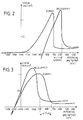
- Fig. 2
- ein Voltamogramm für p-dotiertes unbeleuchtetes und eines für beleuchtetes Silizium in einer Ätzlösung KOH, 30 %, 60° C,
- Fig. 3
- ein Voltamogramm für n-dotiertes unbeleuchtetes und eines für beleuchtetes Silizium in einer Ätzlösung KOH, 30 %, 60° C,
- Fig. 4
- eine perspektivische Ansicht ausgeätzter quaderförmiger Säulen auf einer (100)-Oberfläche des Siliziumkristalls,
- Fig. 5
- eine perspektivische Ansicht eines Silizium-Bauelementes mit Kühlkanälen auf einer (100)-Oberfläche,
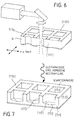
- Fig. 6
- eine perspektivische Ansicht der bisherigen Methode zur Erzeugung von senkrechten (111)-Kristallebenen auf (110)-Siliziumsubstrat,
- Fig. 7
- eine perspektivische Ansicht zur Erzeugung von senkrechten (111)-Silizium-Kristallebenen auf (110)-Oberfläche mittels lichtinduziertem Ätzen,
- Fig. 8a
- eine Draufsicht der Eckenunterätzungen gemäß den Verfahren nach dem Stand der Technik in schematischer Darstellung,
- Fig. 8b
- eine Draufsicht der Eckenunterätzungen am mit einer Schattenmaske abgedeckten Siliziumsubstrat beim lichtinduzierten Ätzen,
- Fig. 9
- ein Schemabild zur Erzeugung einer Membran mit lichtpassiviertem Ätzen, wobei die Dicke der Membran von der Eindringtiefe des Lichtes abhängt.
- Fig. 1
- 2 shows a schematic image of a device for carrying out the proposed light-induced or light-passivated electrochemical etching,
- Fig. 2
- one voltamogram for p-doped non-illuminated and one for illuminated silicon in an etching solution KOH, 30%, 60 ° C,
- Fig. 3
- one voltamogram for n-doped non-illuminated and one for illuminated silicon in an etching solution KOH, 30%, 60 ° C,
- Fig. 4
- 1 shows a perspective view of etched cuboid columns on a (100) surface of the silicon crystal,
- Fig. 5
- 1 shows a perspective view of a silicon component with cooling channels on a (100) surface,
- Fig. 6
- 2 shows a perspective view of the previous method for producing vertical (111) crystal planes on (110) silicon substrate,
- Fig. 7
- 2 shows a perspective view for producing vertical (111) silicon crystal planes on a (110) surface by means of light-induced etching,
- Fig. 8a
- 2 shows a plan view of the corner undercuts according to the methods according to the prior art in a schematic illustration,
- Fig. 8b
- 1 shows a top view of the undercuts on the silicon substrate covered with a shadow mask during the light-induced etching,
- Fig. 9
- a schematic image for producing a membrane with light passivated etching, the thickness of the membrane depends on the depth of penetration of the light.
Intensive Überlegungen und Versuche zur Spannungsabhängigkeit des Ätzens führten zu dem Ergebnis, daß bei p-dotierten Siliziumproben, welche sich auf einem Ätzstoppotential befinden, durch eine Bestrahlung mit Licht, ein Wiederbeginn des Ätzens hervorgerufen wird. Hierbei liegen die lichtinduzierten Ätzraten in der Größenordnung des spannungslosen Ätzens. Durch selektive Bestrahlung des Substrates mit Hilfe einer Maske oder mit Hilfe eines fokussierten Laserstrahles kann der Ätzprozeß auch örtlich selektiv ausgelöst werden. An beleuchteten Stellen wird das Ätzen induziert, dagegen in abgeschatteten Regionen bleibt das Material passiviert.Intensive considerations and experiments on the voltage dependency of the etching led to the result that, in the case of p-doped silicon samples which are at an etching stop potential, by irradiation with light, etching is restarted. Here, the light-induced etching rates are in the order of magnitude of the voltage-free etching. The etching process can also be triggered locally selectively by selective irradiation of the substrate with the aid of a mask or with the aid of a focused laser beam. Etching is induced in illuminated areas, whereas the material remains passivated in shaded regions.
In Fig. 1 ist ein prinzipieller elektrochemischer Aufbau einer Ätzapparatur skizziert. Diese besteht aus einem Ätzgefäß 12, in dem sich eine Referenzelektrode 15 - beispielsweise aus Hg/HgO - , eine Gegenelektrode 16 - beispielsweise aus Pt - , eine Siliziumprobe 13 als Arbeitselektrode und der Elektrolyt 18 - beispielsweise KOH - befinden. Die genannten Elektroden 13, 15, 16 werden über einen Potentiostaten 17 angesteuert. Als Lichtquelle 11 dient ein optischer Aufbau, der für eine weitgehend gleichmäßige, parallele Bestrahlung des Siliziumsubstrats sorgt. Die Selektivität der Beleuchtung wird durch eine Schattenmaske 14 erzeugt, die sich unmittelbar auf der Siliziumscheibe befindet, beispielsweise in Form einer metallischen Dünnfilmbeschichtung.1 shows a basic electrochemical structure of an etching apparatus. This consists of an
Alternativ kann als Strahlungsquelle auch ein fokussierbarer Laserstrahl eingesetzt werden, der rechnergesteuert die Scheibe mit dem gewünschten Muster abrastert (Fig. 4 bis 7). Für die Strahlungsquelle gilt die Forderung, daß sie entsprechend der Bandlücke des Siliziums eine Lichtwellenlänge kleiner als 1,1 µm besitzt. Somit ist also normales sichtbares Licht verwendbar.Alternatively, a focusable laser beam can also be used as the radiation source, which computer-controlled scans the pane with the desired pattern (FIGS. 4 to 7). The requirement for the radiation source is that, according to the band gap of the silicon, it has a light wavelength of less than 1.1 μm. So normal visible light can be used.
Die Fig. 2 zeigt die Darstellung zweier Voltamogramme bei p-dotiertem Silizium mit und ohne Lichteinwirkung, bei denen die Verschiebung des Ätzstoppotentials deutlich zu erkennen ist. Die Weite der Verschiebung hängt von der Intensität des eingestrahlten Lichtes ab. Um den Effekt richtig auszunutzen, muß die angelegte Spannung genau zwischen den beiden Stoppotentialen gewählt werden.2 shows the representation of two voltamograms with p-doped silicon with and without exposure to light, in which the shift in the etching stop potential can be clearly seen. The extent of the shift depends on the intensity of the incident light. In order to take full advantage of the effect, the voltage applied must be selected exactly between the two stop potentials.
Der umgekehrte Effekt liegt bei n-dotiertem Silizium vor. Dort wird bei geeigneter Wahl der Vorspannung der bereits laufende Ätzvorgang durch eine Einstrahlung von Licht gestoppt. Das dazugehörige Paar von Voltamogrammen ist in Fig. 3 dargestellt. Auch hier ist eine Verschiebung des Ätzstoppotentials durch die Einwirkung von Licht gegeben, allerdings diesmal in entgegengesetzter Richtung, verglichen mit p-Silizium.The reverse effect occurs with n-doped silicon. There, with a suitable choice of the bias voltage, the etching process already in progress is stopped by irradiation with light. The associated pair of voltamograms is shown in FIG. 3. Here too there is a shift in the etching stop potential due to the action of light, but this time in the opposite direction compared to p-silicon.
Durch dieses lichtgesteuerte selektive Ätzen ist vor allem im Bereich der Mikromechanik wie auch in der Mikroelektronik eine Vielfältigkeit zur Herstellung von Mikrostrukturen und Bauelementen geschaffen worden, für die nachstehende Ausführungsbeispiele zeugen sollen.This light-controlled, selective etching has created a diversity, particularly in the field of micromechanics as well as in microelectronics, for the production of microstructures and components, for which the following exemplary embodiments are intended to testify.
Auf Siliziumscheiben der Kristallorientierung (100) lassen sich mit Hilfe von hochprozentigen KOH-Lösungen Strukturen mit vertikalen (100)-Ebenen als Seitenbegrenzungen bzw. -wandungen erzeugen. Ohne Einsatz des erfindungsgemäßen Verfahrens ist der laterale Unterätzeffekt jedoch gleichgroß wie der vertikale, so daß keine hohen Aspektverhältnisse in reproduzierbarer Weise erzielbar sind. Mit Hilfe des hier vorgeschlagenen lichtinduzierten Ätzverfahrens kann die vertikale Ätzrate gegenüber der lateralen jedoch wesentlich erhöht werden. Nunmehr können quaderförmige Säulenstrukturen - wie sie beispielsweise die Fig. 4 veranschaulicht - mit gut definierten, vertikalen Seitenwänden erzeugt werden.Structures with vertical (100) planes as side boundaries or walls can be produced on silicon wafers with crystal orientation (100) using high-proof KOH solutions. Without using the method according to the invention, however, the lateral undercut effect is the same size as the vertical one, so that high aspect ratios cannot be achieved in a reproducible manner. With the aid of the light-induced etching method proposed here, however, the vertical etching rate can be significantly increased compared to the lateral one. Cuboid column structures - as illustrated for example in FIG. 4 - can now be produced with well-defined, vertical side walls.
Eine analoge Anwendung veranschaulicht die Fig. 5. Hier werden nach dem vorgeschlagenen Verfahren erzeugte Kühlkanäle für Laserspiegel, Solarzellen oder ähnlich fein zu strukturierende Bauelemente gezeigt. Darüberhinaus ist die Erzeugung von ca. 1 µm schmalen Trenchgräben zur Anordnung von Isolationsgräben für Hochleistungsbauelemente möglich. Diese werden bisher mit üblichen bekannten Trockenätzverfahren hergestellt, wobei es sehr schwierig ist, Gräben mit hohen Aspektverhältnissen und guter Flankensteilheit zu erzielen.FIG. 5 shows an analogous application. Here, cooling channels for laser mirrors, solar cells or similarly fine-structured components are shown, which are produced according to the proposed method. In addition, it is possible to produce trench trenches with a width of approx. 1 µm for the arrangement of isolation trenches for high-performance components. So far, these have been produced using customary known dry etching methods, it being very difficult to achieve trenches with high aspect ratios and good slope steepness.
Ein weiteres Beispiel ist die Erzeugung von vertikalen Schächten in Siliziumscheiben der Orientierung (110). Beim Stand der Technik ist dies nur möglich, wenn zunächst ein Loch mit einem Laserstrahl vorgebohrt wird, wobei das Material verdampft (Fig. 6). Durch das hier vorgeschlagene Verfahren kann nunmehr das anisotrope Durchätzen mit Hilfe einer großflächigen Bestrahlung und einer entsprechenden Schattenmaske problemlos und exakt durchgeführt werden (Fig. 7).Another example is the creation of vertical shafts in silicon wafers of orientation (110). In the prior art, this is only possible if a hole is first pre-drilled with a laser beam, the material evaporating (FIG. 6). With the method proposed here, the anisotropic etching can now be carried out easily and precisely with the aid of large-area irradiation and a corresponding shadow mask (FIG. 7).
Bei der Erzeugung von mikromechanischen Mesastrukturen tritt generell das Problem der Unterätzung an konvexen Ecken auf, wie die Fig. 8a veranschaulicht. Dies ist beispielsweise beim Strukturieren der seismischen Masse eines mikromechanischen Beschleunigungssensors der Fall. Auch hier bringt eine intransparente Schattenmaske - beispielsweise ein metallischer Dünnfilm - und die Beleuchtung bei gleichzeitigem Dunkel-Passivierungspotential eine ganz wesentlich Verbesserung (Fig. 8b).When generating micromechanical mesa structures, the problem of undercutting at convex corners generally arises, as illustrated in FIG. 8a. This is the case, for example, when structuring the seismic mass of a micromechanical acceleration sensor. Here, too, an opaque shadow mask - for example a metallic thin film - and the lighting with simultaneous dark passivation potential bring a very significant improvement (Fig. 8b).
Es darf festgestellt werden, daß nunmehr der Ätzvorgang weitgehend unabhängig von der Kristallographie ist und eine Anisotropie zwischen schnelleren vertikalen und langsameren lateralen Ätzrichtungen erzielt wird. Das bedeutet, daß sich eine planare Schattenmaske mit sehr geringer seitlicher Unterätzung, natürlich bei geeigneter Justierung, in die Tiefe "abbilden" läßt. Dabei erscheinen Tiefen von der Dicke des Siliziumsubstrates erreichbar.It may be stated that the etching process is now largely independent of the crystallography and an anisotropy between faster vertical and slower lateral etching directions is achieved. This means that a planar shadow mask with very little lateral undercut, of course with suitable adjustment, can be "depicted" in depth. Depths of the thickness of the silicon substrate appear to be achievable.
Neue Möglichkeiten sind auch durch den vorbeschriebenen zweiten Effekt des Verfahrens gegeben. Es kann beispielsweise die Dicke einer Membran durch die Eindringtiefe des Lichts in das Material gesteuert werden, wie die Fig. 9 veranschaulicht. Die bisher aufwendige und teuere Epitaxie zur Membranerzeugung entfällt nunmehr.The previously described second effect of the method also opens up new possibilities. For example, the thickness of a membrane can be controlled by the depth of penetration of light into the material, as illustrated in FIG. 9. The previously complex and expensive epitaxy for membrane production is now a thing of the past.
Die vorgenannten Beispiele zeigen die Vielfältigkeit der Anwendungsmöglichkeiten, die jedoch damit bei weitem noch nicht ausgeschöpft sind. So ist beispielsweise auch die Erzeugung von Trenchgräben bei der Kondensatorherstellung in der Höchstintegration möglich, deren Form nunmehr mit kantigem Querschnitt herstellbar ist.The above examples show the variety of possible applications, but they are far from exhausted. For example, it is also possible to produce trench trenches in the manufacture of capacitors with maximum integration, the shape of which can now be produced with an angular cross section.
Claims (8)
Applications Claiming Priority (2)
| Application Number | Priority Date | Filing Date | Title |
|---|---|---|---|
| DE4036895 | 1990-11-20 | ||
| DE19904036895 DE4036895A1 (en) | 1990-11-20 | 1990-11-20 | ELECTROCHEMICAL METHOD FOR ANISOTROPICALLY EATING SILICON |
Publications (2)
| Publication Number | Publication Date |
|---|---|
| EP0486873A1 true EP0486873A1 (en) | 1992-05-27 |
| EP0486873B1 EP0486873B1 (en) | 1997-05-14 |
Family
ID=6418584
Family Applications (1)
| Application Number | Title | Priority Date | Filing Date |
|---|---|---|---|
| EP91118871A Expired - Lifetime EP0486873B1 (en) | 1990-11-20 | 1991-11-06 | Electrochemical method for anisotropic etching of silicon |
Country Status (3)
| Country | Link |
|---|---|
| EP (1) | EP0486873B1 (en) |
| JP (1) | JP3187885B2 (en) |
| DE (1) | DE4036895A1 (en) |
Cited By (1)
| Publication number | Priority date | Publication date | Assignee | Title |
|---|---|---|---|---|
| US5338415A (en) * | 1992-06-22 | 1994-08-16 | The Regents Of The University Of California | Method for detection of chemicals by reversible quenching of silicon photoluminescence |
Families Citing this family (7)
| Publication number | Priority date | Publication date | Assignee | Title |
|---|---|---|---|---|
| EP0630058A3 (en) * | 1993-05-19 | 1995-03-15 | Siemens Ag | Process for forming an arrangement of pyrodetectors by electrochemically etching a silicon substrate. |
| DE4328628A1 (en) * | 1993-08-20 | 1994-01-20 | Ulrich Prof Dr Mohr | Electrolytic production of standard oxide layer on silicon bodies - using focussed laser beam to heat areas where oxide is to be produced |
| DE19710375C2 (en) * | 1997-03-13 | 2002-11-07 | Micronas Semiconductor Holding | Process for the production of spatially structured components |
| DE102004037128A1 (en) * | 2004-07-30 | 2006-03-23 | Robert Bosch Gmbh | Micromechanical assembly part structuring method, involves removing material of micromechanical assembly part e.g. semiconductor substrate, by laser treatment that produces diaphragm in assembly part |
| US7494936B2 (en) * | 2005-05-16 | 2009-02-24 | Technion Research & Development Foundation Ltd. | Method for electrochemical etching of semiconductor material using positive potential dissolution (PPD) in solutions free from hydrogen fluoride (HF) |
| US20070256937A1 (en) * | 2006-05-04 | 2007-11-08 | International Business Machines Corporation | Apparatus and method for electrochemical processing of thin films on resistive substrates |
| CN113930846A (en) * | 2021-12-15 | 2022-01-14 | 南京日托光伏新能源有限公司 | Method for making wool by matching sodium hydroxide single crystals |
Citations (4)
| Publication number | Priority date | Publication date | Assignee | Title |
|---|---|---|---|---|
| FR2070873A1 (en) * | 1969-12-16 | 1971-09-17 | Western Electric Co | |
| EP0037876A2 (en) * | 1980-03-27 | 1981-10-21 | International Business Machines Corporation | Electrochemical eroding process for semiconductors |
| US4369099A (en) * | 1981-01-08 | 1983-01-18 | Bell Telephone Laboratories, Incorporated | Photoelectrochemical etching of semiconductors |
| US4482443A (en) * | 1983-12-30 | 1984-11-13 | At&T Technologies | Photoelectrochemical etching of n-type silicon |
Family Cites Families (1)
| Publication number | Priority date | Publication date | Assignee | Title |
|---|---|---|---|---|
| US4414066A (en) * | 1982-09-10 | 1983-11-08 | Bell Telephone Laboratories, Incorporated | Electrochemical photoetching of compound semiconductors |
-
1990
- 1990-11-20 DE DE19904036895 patent/DE4036895A1/en active Granted
-
1991
- 1991-11-06 EP EP91118871A patent/EP0486873B1/en not_active Expired - Lifetime
- 1991-11-14 JP JP29910191A patent/JP3187885B2/en not_active Expired - Fee Related
Patent Citations (4)
| Publication number | Priority date | Publication date | Assignee | Title |
|---|---|---|---|---|
| FR2070873A1 (en) * | 1969-12-16 | 1971-09-17 | Western Electric Co | |
| EP0037876A2 (en) * | 1980-03-27 | 1981-10-21 | International Business Machines Corporation | Electrochemical eroding process for semiconductors |
| US4369099A (en) * | 1981-01-08 | 1983-01-18 | Bell Telephone Laboratories, Incorporated | Photoelectrochemical etching of semiconductors |
| US4482443A (en) * | 1983-12-30 | 1984-11-13 | At&T Technologies | Photoelectrochemical etching of n-type silicon |
Non-Patent Citations (4)
| Title |
|---|
| IEEE TRANSACTIONS ON ELECTRON DEVICES Bd. 36, Nr. 4, April 1989, NEW YORK US Seiten 663 - 669; BEN KLOECK ET AL.: 'Study of electrochemical etch-stop for high-precision thickness control of Silicon membranes' * |
| JOURNAL OF THE ELECTROCHEMICAL SOCIETY. Bd. 131, Nr. 1, Januar 1984, MANCHESTER, NEW HAMPSHIRE US Seiten 27 - 34; EDOUARD HAROUTIOUNIAN ET AL.: 'Electrochemical and photoelectrochemical behavior and selective etching of III-V semiconductors in H2O2 as redox system' * |
| JOURNAL OF VACUUM SCIENCE AND TECHNOLOGY: PART B. Bd. 1, Nr. 1, Januar 1983, NEW YORK US Seiten 48 - 53; S. MENEZES ET AL.: 'Electrodissolution and passivation phenomena in III-V semiconducting compounds' * |
| PATENT ABSTRACTS OF JAPAN vol. 9, no. 31 (E-295)9. Februar 1985 & JP-A-59 175 127 ( DAINIPPON INSATSU K.K. ) 3. Oktober 1984 * |
Cited By (1)
| Publication number | Priority date | Publication date | Assignee | Title |
|---|---|---|---|---|
| US5338415A (en) * | 1992-06-22 | 1994-08-16 | The Regents Of The University Of California | Method for detection of chemicals by reversible quenching of silicon photoluminescence |
Also Published As
| Publication number | Publication date |
|---|---|
| JP3187885B2 (en) | 2001-07-16 |
| EP0486873B1 (en) | 1997-05-14 |
| DE4036895A1 (en) | 1992-05-21 |
| DE4036895C2 (en) | 1993-03-11 |
| JPH04267524A (en) | 1992-09-24 |
Similar Documents
| Publication | Publication Date | Title |
|---|---|---|
| DE69433361T2 (en) | Manufacturing method of self-assembling microstructures | |
| DE19921241B4 (en) | A method of manufacturing a semiconductor sensor for a dynamic quantity | |
| DE4402085C2 (en) | Process for the micro-technical production of a capacitive differential pressure sensor and micro-technical differential pressure sensor | |
| DE4341271B4 (en) | Crystalline material acceleration sensor and method of making this acceleration sensor | |
| DE69839042T2 (en) | TILED LAYER WITH HIGH CONDUCTIVITY IN AN OPTICAL WAVEGUIDE | |
| DE602004012590T2 (en) | METHOD AND SYSTEMS FOR PROVIDING MEMS DEVICES WITH A TOP CAP AND UPPER RECORD PLATE | |
| DE4331798B4 (en) | Process for the production of micromechanical components | |
| EP1334060A1 (en) | Micromechanical component and corresponding production method | |
| DE4016472C2 (en) | ||
| WO2001046066A2 (en) | Sensor with at least one micromechanical structure and method for the production thereof | |
| EP0296348A1 (en) | Process for etching holes or grooves in n-type silicium | |
| DE4000496A1 (en) | METHOD FOR STRUCTURING A SEMICONDUCTOR BODY | |
| EP1373129A2 (en) | Method for producing micromechanic sensors and sensors produced by said method | |
| EP1345842A2 (en) | Method for producing a semiconductor component having a movable mass in particular, and semiconductor component produced according to this method | |
| DE4030466C2 (en) | Piezo resistance device | |
| EP0486873B1 (en) | Electrochemical method for anisotropic etching of silicon | |
| DE4318466A1 (en) | Micromechanical sensor and method for its production | |
| DE4106287A1 (en) | METHOD FOR ANISOTROPICALLY ASSEMBLING MONOCRISTALLINE, DISC-SHAPED CARRIERS | |
| DE4106933B4 (en) | patterning methods | |
| DE19527314A1 (en) | Fabrication of silicon membrane with predefined parameters | |
| DE102008026886B4 (en) | Process for structuring a wear layer of a substrate | |
| EP0514395A1 (en) | Crystal-oriented motion sensor and process for manufacturing it | |
| DE102004043357B4 (en) | Method for producing a micromechanical sensor element | |
| DE19603829A1 (en) | Silicon@ based micromechanical structure manufacturing method | |
| EP1546029A1 (en) | Method for the production of a micromechanical device, particularly a micromechanical oscillating mirror device |
Legal Events
| Date | Code | Title | Description |
|---|---|---|---|
| PUAI | Public reference made under article 153(3) epc to a published international application that has entered the european phase |
Free format text: ORIGINAL CODE: 0009012 |
|
| AK | Designated contracting states |
Kind code of ref document: A1 Designated state(s): FR GB IT |
|
| 17P | Request for examination filed |
Effective date: 19920617 |
|
| 17Q | First examination report despatched |
Effective date: 19921026 |
|
| RAP1 | Party data changed (applicant data changed or rights of an application transferred) |
Owner name: DEUTSCHE AEROSPACE AKTIENGESELLSCHAFT |
|
| RAP1 | Party data changed (applicant data changed or rights of an application transferred) |
Owner name: DAIMLER-BENZ AEROSPACE AKTIENGESELLSCHAFT |
|
| GRAG | Despatch of communication of intention to grant |
Free format text: ORIGINAL CODE: EPIDOS AGRA |
|
| GRAH | Despatch of communication of intention to grant a patent |
Free format text: ORIGINAL CODE: EPIDOS IGRA |
|
| GRAH | Despatch of communication of intention to grant a patent |
Free format text: ORIGINAL CODE: EPIDOS IGRA |
|
| RAP1 | Party data changed (applicant data changed or rights of an application transferred) |
Owner name: DAIMLER-BENZ AKTIENGESELLSCHAFT |
|
| GRAA | (expected) grant |
Free format text: ORIGINAL CODE: 0009210 |
|
| AK | Designated contracting states |
Kind code of ref document: B1 Designated state(s): FR GB IT |
|
| GBT | Gb: translation of ep patent filed (gb section 77(6)(a)/1977) |
Effective date: 19970515 |
|
| ET | Fr: translation filed | ||
| PLBE | No opposition filed within time limit |
Free format text: ORIGINAL CODE: 0009261 |
|
| STAA | Information on the status of an ep patent application or granted ep patent |
Free format text: STATUS: NO OPPOSITION FILED WITHIN TIME LIMIT |
|
| 26N | No opposition filed | ||
| REG | Reference to a national code |
Ref country code: GB Ref legal event code: 732E |
|
| REG | Reference to a national code |
Ref country code: FR Ref legal event code: TP |
|
| PGFP | Annual fee paid to national office [announced via postgrant information from national office to epo] |
Ref country code: GB Payment date: 20011012 Year of fee payment: 11 |
|
| PGFP | Annual fee paid to national office [announced via postgrant information from national office to epo] |
Ref country code: FR Payment date: 20011106 Year of fee payment: 11 |
|
| REG | Reference to a national code |
Ref country code: GB Ref legal event code: IF02 |
|
| PG25 | Lapsed in a contracting state [announced via postgrant information from national office to epo] |
Ref country code: GB Free format text: LAPSE BECAUSE OF NON-PAYMENT OF DUE FEES Effective date: 20021106 |
|
| GBPC | Gb: european patent ceased through non-payment of renewal fee | ||
| PG25 | Lapsed in a contracting state [announced via postgrant information from national office to epo] |
Ref country code: FR Free format text: LAPSE BECAUSE OF NON-PAYMENT OF DUE FEES Effective date: 20030731 |
|
| REG | Reference to a national code |
Ref country code: FR Ref legal event code: ST |
|
| PG25 | Lapsed in a contracting state [announced via postgrant information from national office to epo] |
Ref country code: IT Free format text: LAPSE BECAUSE OF NON-PAYMENT OF DUE FEES;WARNING: LAPSES OF ITALIAN PATENTS WITH EFFECTIVE DATE BEFORE 2007 MAY HAVE OCCURRED AT ANY TIME BEFORE 2007. THE CORRECT EFFECTIVE DATE MAY BE DIFFERENT FROM THE ONE RECORDED. Effective date: 20051106 |