EP0486332B1 - Operational amplifier - Google Patents
Operational amplifier Download PDFInfo
- Publication number
- EP0486332B1 EP0486332B1 EP91402659A EP91402659A EP0486332B1 EP 0486332 B1 EP0486332 B1 EP 0486332B1 EP 91402659 A EP91402659 A EP 91402659A EP 91402659 A EP91402659 A EP 91402659A EP 0486332 B1 EP0486332 B1 EP 0486332B1
- Authority
- EP
- European Patent Office
- Prior art keywords
- output
- differential
- common mode
- stage
- gain stages
- Prior art date
- Legal status (The legal status is an assumption and is not a legal conclusion. Google has not performed a legal analysis and makes no representation as to the accuracy of the status listed.)
- Expired - Lifetime
Links
- 239000003990 capacitor Substances 0.000 claims description 24
- 230000008878 coupling Effects 0.000 claims description 8
- 238000010168 coupling process Methods 0.000 claims description 8
- 238000005859 coupling reaction Methods 0.000 claims description 8
- 230000003321 amplification Effects 0.000 description 12
- 238000003199 nucleic acid amplification method Methods 0.000 description 12
- 238000010586 diagram Methods 0.000 description 7
- 238000006243 chemical reaction Methods 0.000 description 4
- 238000000034 method Methods 0.000 description 4
- 238000005516 engineering process Methods 0.000 description 3
- 230000006978 adaptation Effects 0.000 description 2
- 230000000295 complement effect Effects 0.000 description 2
- 229910044991 metal oxide Inorganic materials 0.000 description 2
- 150000004706 metal oxides Chemical class 0.000 description 2
- 239000004065 semiconductor Substances 0.000 description 2
- 230000003247 decreasing effect Effects 0.000 description 1
- 238000007667 floating Methods 0.000 description 1
- 238000009499 grossing Methods 0.000 description 1
- 230000003071 parasitic effect Effects 0.000 description 1
- 238000005070 sampling Methods 0.000 description 1
- 239000007787 solid Substances 0.000 description 1
Images

Classifications
-
- H—ELECTRICITY
- H03—ELECTRONIC CIRCUITRY
- H03F—AMPLIFIERS
- H03F3/00—Amplifiers with only discharge tubes or only semiconductor devices as amplifying elements
- H03F3/30—Single-ended push-pull [SEPP] amplifiers; Phase-splitters therefor
- H03F3/3001—Single-ended push-pull [SEPP] amplifiers; Phase-splitters therefor with field-effect transistors
- H03F3/3061—Bridge type, i.e. two complementary controlled SEPP output stages
- H03F3/3062—Bridge type, i.e. two complementary controlled SEPP output stages with asymmetrical driving of the end stage
-
- H—ELECTRICITY
- H03—ELECTRONIC CIRCUITRY
- H03F—AMPLIFIERS
- H03F3/00—Amplifiers with only discharge tubes or only semiconductor devices as amplifying elements
- H03F3/30—Single-ended push-pull [SEPP] amplifiers; Phase-splitters therefor
- H03F3/3001—Single-ended push-pull [SEPP] amplifiers; Phase-splitters therefor with field-effect transistors
- H03F3/3022—CMOS common source output SEPP amplifiers
- H03F3/3023—CMOS common source output SEPP amplifiers with asymmetrical driving of the end stage
-
- H—ELECTRICITY
- H03—ELECTRONIC CIRCUITRY
- H03F—AMPLIFIERS
- H03F3/00—Amplifiers with only discharge tubes or only semiconductor devices as amplifying elements
- H03F3/45—Differential amplifiers
- H03F3/45071—Differential amplifiers with semiconductor devices only
- H03F3/45076—Differential amplifiers with semiconductor devices only characterised by the way of implementation of the active amplifying circuit in the differential amplifier
- H03F3/45179—Differential amplifiers with semiconductor devices only characterised by the way of implementation of the active amplifying circuit in the differential amplifier using MOSFET transistors as the active amplifying circuit
- H03F3/45183—Long tailed pairs
- H03F3/45192—Folded cascode stages
-
- H—ELECTRICITY
- H03—ELECTRONIC CIRCUITRY
- H03F—AMPLIFIERS
- H03F3/00—Amplifiers with only discharge tubes or only semiconductor devices as amplifying elements
- H03F3/45—Differential amplifiers
- H03F3/45071—Differential amplifiers with semiconductor devices only
- H03F3/45076—Differential amplifiers with semiconductor devices only characterised by the way of implementation of the active amplifying circuit in the differential amplifier
- H03F3/45475—Differential amplifiers with semiconductor devices only characterised by the way of implementation of the active amplifying circuit in the differential amplifier using IC blocks as the active amplifying circuit
-
- H—ELECTRICITY
- H03—ELECTRONIC CIRCUITRY
- H03F—AMPLIFIERS
- H03F3/00—Amplifiers with only discharge tubes or only semiconductor devices as amplifying elements
- H03F3/45—Differential amplifiers
- H03F3/45071—Differential amplifiers with semiconductor devices only
- H03F3/45479—Differential amplifiers with semiconductor devices only characterised by the way of common mode signal rejection
- H03F3/45632—Differential amplifiers with semiconductor devices only characterised by the way of common mode signal rejection in differential amplifiers with FET transistors as the active amplifying circuit
- H03F3/45636—Differential amplifiers with semiconductor devices only characterised by the way of common mode signal rejection in differential amplifiers with FET transistors as the active amplifying circuit by using feedback means
- H03F3/45641—Measuring at the loading circuit of the differential amplifier
- H03F3/45659—Controlling the loading circuit of the differential amplifier
-
- H—ELECTRICITY
- H03—ELECTRONIC CIRCUITRY
- H03F—AMPLIFIERS
- H03F3/00—Amplifiers with only discharge tubes or only semiconductor devices as amplifying elements
- H03F3/45—Differential amplifiers
- H03F3/45071—Differential amplifiers with semiconductor devices only
- H03F3/45479—Differential amplifiers with semiconductor devices only characterised by the way of common mode signal rejection
- H03F3/45928—Differential amplifiers with semiconductor devices only characterised by the way of common mode signal rejection using IC blocks as the active amplifying circuit
- H03F3/45932—Differential amplifiers with semiconductor devices only characterised by the way of common mode signal rejection using IC blocks as the active amplifying circuit by using feedback means
- H03F3/45937—Measuring at the loading circuit of the differential amplifier
- H03F3/45946—Controlling the loading circuit of the differential amplifier
-
- H—ELECTRICITY
- H03—ELECTRONIC CIRCUITRY
- H03F—AMPLIFIERS
- H03F2200/00—Indexing scheme relating to amplifiers
- H03F2200/153—Feedback used to stabilise the amplifier
-
- H—ELECTRICITY
- H03—ELECTRONIC CIRCUITRY
- H03F—AMPLIFIERS
- H03F2203/00—Indexing scheme relating to amplifiers with only discharge tubes or only semiconductor devices as amplifying elements covered by H03F3/00
- H03F2203/45—Indexing scheme relating to differential amplifiers
- H03F2203/45471—Indexing scheme relating to differential amplifiers the CSC comprising one or more extra current sources
Definitions
- the present invention relates in general to analog circuitry and more particularly to an operational amplifier and method of amplification.
- Oversampling conversion techniques allow for a reduction in the amount of analog circuitry required in analog-to-digital and digital-to-analog converters by shifting most of the digital processing functions into the digital domain.
- oversampling conversion techniques the need for analog circuitry is no! completely eliminated.
- Those analog elements still necessary for the implementation of oversampling conversion, such as operational amplifiers, must meet stringent performance requirements, especially in light of the high sampling frequency required.
- these analog elements must be compatible with the technology used to fabricate the associated digital integrated circuits such that both the analog and digital functions can be integrated into a single high-density chip. For example, if complementary metal oxide semiconductor (CMOS) digital circuitry is being used, the associated analog circuit elements must be fabricated using CMOS technology or CMOS compatible technology.
- CMOS complementary metal oxide semiconductor
- Complementary metal oxide semiconductor (CMOS) over-sampled converters typically include continuous parts, such as RC anti-aliasing and smoothing filters, directly connected to switched capacitors being sampled at high-frequency, typically in the range of 1-10 MHz.
- CMOS converters implement CMOS operational amplifiers for switched capacitor filters which are generally based on single-stage transconductance amplifier structures. While single-stage transconductance operational amplifier structures have speed characteristics suitable for oversampled converters, these structures present a very high output impedance such that they are not well adapted to driving resistive loads. Further, the output stages of currently available CMOS amplifiers typically consist of several transistors connected in series, a structure which limits the available output voltage swing. A consequence of reduced output voltage swing is decreased output linearity and signal-to-noise ratio performance.
- EP-A-0 325 299 discloses an amplifier with differential inputs and single ended outputs.
- EP-A-3 725 323 discloses an amplifier having differential inputs and outputs with a very complex structure.
- CMOS operational amplifier adapted to the performance required for oversampled converters.
- the need has arisen for a high-speed operational amplifier having high output linearity, improved signal to noise ration performance at the output, and having a reduced output impedance capable of driving resistive loads.
- an improved operational amplifier as defined in the appended independent claim 1 is provided.
- the differential path comprises a first gain stage coupled to the input stage, a second gain stage coupled the first gain stage and circuitry coupled to the output terminals and the second gain stage for dynamically controlling the output bias current from the second gain stage.
- the common mode loop includes the first gain stage, the second gain stage and a common mode input stage coupling the output terminals and the first gain stage.
- the present invention has significant advantages over prior art of CMOS operational amplifiers.
- the present invention has the speed necessary for use in oversampled analog to digital and digital to analog converters. Further, the reduced output impedance allows the operational amplifier of the present invention to drive both resistive and capacitive loads. Additionally, the operational amplifier of the present invention avoids the slew rate mode during switching transients. Finally, the present invention provides both a switchable power down mode and an unlockable common mode control loop at power up.
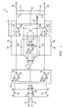
- FIGURE 1 is a block diagram of a high performance operational amplifier 10 according to the present invention.
- Operational amplifier 10 includes a noninverting input 12 and an inverting input 14.
- Noninverting input 12 is coupled to the noninverting input 16 of first (input) stage 18 and the first plate 20 of capacitor 22.
- Inverting input 14 is coupled to the inverting input 24 of first (input) stage circuitry 18 and the first plate 26 of capacitor 28.
- the second stage of operational amplifier 10 (the first amplifying stage) is a cascode amplifier and is shown generally by dotted lines at 30.
- Second stage 30 includes an upper section 32 and a lower section 34.
- the noninverting input 36 of upper section 32 is coupled to the inverting output 38 of input stage 18.
- Noninverting input 36 is also coupled to second plate 40 of capacitor 28.
- the inverting input 42 of section 32 is coupled to the inverting input 44 of lower section 34.
- the noninverting input 46 of lower section 34 is coupled to the noninverting output of input stage 18 and second plate 50 of capacitor 22.
- Inverting input 42 of upper stage 32 and inverting input 44 of lower stage 34 are each connected to output 52 of third stage 54.
- the noninverting input of third stage 54 is coupled to a reference voltage V cmref at node 58.
- the noninverting input of third stage 54 is coupled to feedback node 62.
- Third stage 54 operates as the input stage of a common mode loop which sets the operating point of amplifier 10 by maintaining the mean output voltage of amplifier 10 at a preselected common mode voltage.
- the fourth stage (the second amplifying stage) is shown by dotted lines generally at 64 and includes an upper section 66 and a lower section 68.
- the output 70 of upper section 32 of second stage 30 is coupled to inverting input 72 of upper section 66 of fourth stage 64.
- the output 74 of lower section 34 of second stage 30 is coupled to inverting input 76 of lower section 68 of fourth section 64.
- the output 78 of upper section 66 is coupled to noninverting output 80 of amplifier 10 while the output 82 of lower section 68 is coupled to inverting output 84 of amplifier 10.
- Output current is dynamically controlled with a loop including fifth stage 86 (the auxiliary stage).
- Output 70 of upper section 32 of second stage 30 is coupled to noninverting input 88 of fifth stage 86.
- Output 74 of lower section 34 of second stage 30 is coupled to inverting input 94 of fifth stage 86.
- Noninverting output terminal 80 is coupled to noninverting input 88 of fifth stage 86 through a capacitor 90 and resistor 92.
- inverting output terminal 84 is coupled to inverting input 94 of fifth stage 86 through a capacitor 96 and a resistor 98.
- Fifth stage 86 includes a noninverting output 100 and an inverting output 102.
- Noninverting output 100 is coupled to an input 104 of upper stage 66 of fourth stage 64.
- a capacitor 106 couples noninverting output 100 to noninverting input 88 of fifth stage 86.
- Noninverting output 102 is coupled to an input 108 of lower section 68 of fourth stage 64.
- a feedback capacitor 110 coupled inverting output 102 of fifth stage 86 to inverting input 94.
- noninverting output 80 of amplifier 10 is coupled to node 62 and the input 60 of third stage 54 by a parallel combination of capacitor 112 and resistor 114.
- noninverting output terminal 84 is coupled through node 62 and input 60 of third stage 54 by the parallel combination of capacitor 116 and resistor 118.
- input stage 18 comprises a differential amplifier at inputs 16 and 24 of input stage 18 such that the receipt of unbalanced differential signals result in similarly unbalanced output signals appearing on inverting output 38 and noninverting output 48.
- the amplified differential signals output from each output of input stage 18 are then fed to the respective noninverting inputs 36 and 46 of amplification stages 32 and 34.
- amplification stages 32 and 34 comprise cascode amplification stages whose outputs are driven from first and second voltage rails.
- the respective differential signals are then further amplified through second stage amplification sections 66 and 68.
- amplification section 66 and 68 comprise common source amplifiers whose outputs are also driven from the first and second voltage rails.
- Amplifier section 66 and 68 invert the polarities of the differential signals, which had been previously inverted by the differential amplifier of input stage 18, such that the outputs at 80 and 84 directly correspond in polarity to the inputs at input terminals 12 and 14.
- the double amplification stage provides increased output drive allowing a greater voltage swing across the load coupled between output terminals 80 and 84.
- Auxiliary section 86 controls the bias currents at the outputs of second stage amplification sections 66 and 68.
- auxiliary stage 86 includes current mirrors coupled at inputs 104 and 108 of respective amplification sections 66 and 68. Functionally, the current mirrors mirror the current through the common source amplifier output transistors.
- Auxiliary section 86 also includes a differential amplifier which drives the current mirrors received from the outputs 70 and 74 of the first amplification sections 32 and 34. When the outputs 70 and 74 of amplification sections are unbalanced the signal provided to inputs 88 and 94 of the differential amplifier of auxiliary stage 86 causes unbalanced drive to the current mirrors.
- the resulting unbalanced current through the current mirrors is in turn reflected in an unbalanced current output from common source amplification section 66 and 68.
- the resulting modulation of the output current allows the circuit to adapt to the current required by the output load, thereby increasing the threshold beyond which the amplifier goes into the slew rate mode.
- the operating point of amplifier 10 is set by maintaining the mean voltage value between output terminals 80 and 84 at the common mode voltage.
- the mean of the output voltages is taken at node 62 which coupled to noninverting output terminal 80 through an impedance comprising capacitor 112 and resistor 114 and to inverting output 84 through the impedance comprising capacitor 116 and resistor 118.
- the mean voltage appearing at node 62 is then fed back to the inverting input of common mode stage 54, the noninverting input 56 of which is tied to a reference voltage V cmref .
- common mode stage 54 comprises a differential amplifier with inputs 56 and 60 being its respective differential inputs.
- the reference voltage controls the balancing of the differential amplifier in essence comparing the reference voltage with the mean output voltage.
- the output of common mode section 54 then provides feedback at the inverting inputs 42 and 44 of first stage amplifying sections 32 and 34 such that the cascode amplifiers making up stages 32 and 34 are biased to set the common mode voltage of outputs 80 and 84.
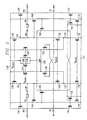
- a schematic diagram depicts the differential path of operational amplifier 10.
- the differential path includes first stage (the input stage) 18, second (the first gain stage) 30, fourth stage (the second gain stage) 64 and stage five 86 which dynamically controls the bias current of fourth stage 64.
- First stage 18 is composed of a pair differential p channel transistors 120 and 122, and a current source made up of transistors 124 and 126.
- Noninverting input terminal 12 of amplifier 10 is coupled to the gate of transistor 120, which is noninverting input 16 for input stage 18.
- Inverting terminal 14 is similarly tied to the gate of transistor 122 which is the noninverting input 24 of input stage 18.
- One source/drain of transistor 120 is coupled to a first source/drain of current p channel source transistor 124.
- the second source/drain of p channel transistor 124 is coupled to first voltage rail 128 while the gate of transistor 124 is coupled to a bias voltage V bias1 .
- a first one of the source/drain of transistor 122 is coupled to the first source/drain of transistor 126.
- the second source/drain region of transistor 126 is coupled to voltage rail 128 while the gate of transistor 126 is coupled to bias voltage V bias1 .
- the first source/drains of differential transistors 120 and 122, and current source transistors 124 and 126 are tied together at node 129.
- the second stage 30 (the first gain stage) includes a cascode amplifier made up of n channel transistors 130, 132, 134 and 136, and p channel transistors 138 and 140.
- the current flowing out of p channel transistor 120 of the first stage 16 modulates the current flowing through the cascode stage consisting of n channel transistors 130 and 134 and the p channel cascode load transistor 138.
- the second source/drain of p channel transistor 120 is coupled to respective first source/drains of n channel transistors 130 and 134 at node 133.
- the second source/drain of transistor 130 is coupled to the first source/drain of p channel transistor 138.
- the gate of transistor 130 is tied to bias voltage V bias2 .
- the second source/drain of n channel transistor 134 is tied to the second voltage rail 131.
- the gate of transistor 134 is tied to bias voltage V bias3 .
- the second source/drain of p channel transistor 138 is coupled to first voltage rail 128 while the gate of transistor 138 is coupled to bias voltage V bias4 .
- the current through p channel transistor 122 modulates the current flowing through the cascode stage including n channel transistors 132 and 136 and p channel load transistor 140.
- the second source/drain of transistor 122 is coupled to the first source/drains of n channel transistors 132 and 136, respectively at node 135.
- the second source/drain of transistor 132 is coupled to the first source/drain of transistor 140 while the gate of transistor 132 is coupled to bias voltage V bias2 .
- the second source/drain of p channel transistor 136 is tied to the second voltage rail 131 while the gate of transistor 136 is coupled to bias voltage V bias3 .
- the second source/drain of p channel transistor 140 is tied to first voltage rail 128 and the gate of transistor 140 coupled to bias voltage V bias4 .
- circuitry of second stage 30 allows for the selection of large sized transistors 134 and 136 which reduces their contributions to noise and offset without reducing the performance of the amplifier.
- the upper section 66 of fourth stage 64 (the second gain stage) is composed of p channel transistor 144 and n channel transistor 146.
- the first source/drain regions of transistors 144 and 146 are tied together and to noninverting output 80.
- the second source/drain of p channel transistor 144 is coupled to first voltage rail 128.
- the gate of transistor 144 is coupled to the second source/drain of transistor 130 ,forming part second stage 30, at node 70.
- the second source/drain of n channel 146 is coupled to second voltage rail 131.
- the lower section 68 of fourth stage 64 includes p channel transistor 148 and n channel transistor 150.
- the respective first source/drains of transistors 148 and 150 are coupled together and coupled to inverting output 84 of amplifier 10.
- the second source/drain of transistor 148 is coupled to first voltage rail 128 while the gate of transistor 148 is coupled to the second source/drain of transistor 132, forming part of second stage 30, at node 72.
- the second source/drain of transistor 150 is coupled to second voltage rail 131.
- the biasing current of the fourth stage 64 is controlled by fifth (auxiliary) stage 86 which allows dynamic adaptation of the current to the differential signal output on terminals 80 and 84.
- a first current mirror is formed by coupling the gate of transistor 146 to the gate and first source/drain of n channel transistor 152. The second source/drain of transistor 152 is coupled to the second voltage rail 131.
- a second current mirror is formed by coupling the gate of n channel transistor 150 to the gate and first source/drain of n channel transistor 154. The second source/drain of n channel transistor is coupled to second voltage rail 131.
- the current biasing for the first and second current mirrors is provided by p channel transistors 156 and 158.
- P channel transistors 156 and 158 are further coupled to p channel differential pair transistors 160 and 162, which along with transistors 152 and 154, complete the auxiliary differential amplifier.
- the first source/drain of n channel transistor 152 is coupled to a first source/drain of transistor 162.
- the second source/drain of transistor 162 is coupled to the first source/drains of p channel transistors 156 and 158.
- the second source/drains of p channel transistors 156 and 158 are coupled to first voltage rail 128 while the gates of transistors 156 and 158 are tied to bias voltage V bias1 .
- first source/drain of n channel transistor 154 is coupled to a first source/drain of p channel transistor 160.
- the second source/drain of p channel transistor 160 is also coupled both to the first source/drains of p channel transistors 156 and 158.
- a pair of voltage followers are forced by transistors 164 and 166, 168 and 170.
- the first source/drains of transistors 164 and 166 are coupled together and to the gate of p channel transistor 160.
- the second source/drain of n channel transistor 164 is coupled to the first voltage rail 128 while the second source/drain of transistor 166 is tied to second voltage rail 131.
- the gate of transistor 164 is coupled to node 70 and the gate of n channel transistor 166 is tied to bias voltage V bias3 .
- the first source/drains of n channel transistors 168 and 170 are coupled together and to the gate of p channel transistor 162.
- the second source/drain of transistor 168 is tied to first voltage rail 128 while the second source/drain of transistor 170 is tied to second voltage rail 131.
- the gate of transistor 168 is tied to node 72 while the gate of transistor 170 is tied to bias voltage V bias3 .
- Noninverting output terminal 80 is coupled to node 70 through capacitor 90 and resistor 92.
- Inverting output 84 is coupled to node 72 through capacitor 96 and resistor 98.
- Transistors 160 and 162 drive transistor 152 and 154 differentially (unbalanced) such that the output currents through transistors 146 and 150 are unequal. This modulation of output current provides for the adaptation of the currents at output terminals 80 and 84 to the associated loads. This increases the threshold beyond which the amplifier goes into the slew rate mode and consequently reduces the non-linearities resulting due to the slew rate phenomenon during transients.
- FIGURE 3 the common mode path for operational amplifier 10 is depicted.
- interconnections previously described in conjunction with the differential path shown in FIGURE 2 will not be repeated here.
- the input stage for the common mode path includes a current source consisting of n channel transistors 172 and 174, a differential pair formed by n channel transistors 176 and 178, and loads consisting of p channel transistors 180 and 182.
- the first source/drains of transistors 172 and 174 are tied to second voltage rail 131 while the gates of transistors 172 and 174 are coupled to bias voltage V bias3 .
- the second source/drain of transistor 172 is coupled to a first source/drain of transistor 176 while the second source/drain of transistor 174 is tied to a first source/drain of transistor 178.
- the gate of transistor 176 is tied to a reference common mode voltage V cmref .
- the gate of transistor 178 is coupled to a signal V cmin , which is equal to the mean value of the two output voltages appearing at output terminals 80 and 84. This mean value can be generated either in a time continuous fashion using resistors 114 and 118, as depicted in FIGURE 1, or in a sampled way by replacing resistors 114 and 118 with switched capacitors.
- the second source/drain of transistor 176 is coupled to the gate and first source/drain of transistor 180 at node 177.
- the second source/drain of transistor 180 is in turn tied to first voltage rail 128.
- the second source/drain of transistor 178 is coupled at node 179 to the gate and first source/drain of p channel transistor 182, the second source/drain of which is tied to voltage rail 128.
- P channel transistor 186 has a first source/drain tied to first voltage rail 128 and a second source/drain coupled to second source/drain of n channel transistor 176.
- P channel transistor 188 has a first source/drain tied to first voltage rail 128 and a second source/drain coupled to the second source/drain of n channel transistor 178.
- the gates of transistors 186 and 188 are each tied to bias voltage V bias1 .
- the common mode path sets the common mode voltage and thereby the operating point of operational amplifier 10.
- the structure of the common mode path is also designed to avoid any locking state and ensure the proper biasing at start-up of the circuit independent of the initial conditions.
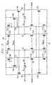
- FIGURE 4 is a schematic diagram of the complete circuitry of operational amplifier 10, including the compensation loops, as well as the differential and common mode paths depicted in FIGURES 2 and 3.
- Overall loop stability is achieved by compensation networks, one of which is the main network used for the compensation of both the differential and common mode paths.
- the main compensation network uses the pole-splitting technique and includes the RC networks formed by capacitor 90 and resistor 92, and capacitor 96 and resistor 98, respectively.
- the main pole location depends on the output conductance of transistors 138 and 140, on the values of capacitors 90 and 96, and on the gain of the output stages formed transistors 144, 146, 148 and 150. Since all the elements required to set the main pole location are shared by both the differential and common mode paths, the same compensation network ensures the stability of the two loops.
- Capacitors 22 and 28 allow compensation of the pole due to the parasitic capacitance on the cascode nodes 133 and 135 when the transconductance ratio of transistors 120 and 130 and 122 and 132 are properly selected.
- Capacitors 106 and 110 are used as feed-forward elements for the fifth stage 54.
- the power-down state is set by opening all the paths allowing current flow between supply rails 128 and 130. This is achieved by turning off most of the active devices and setting values of the internal nodes to a known voltage.
- This function is implemented using p channel transistors 190, 192, 194 and 196, and n channel transistors 198 and 200.
- the gates of p channel transistors 190, 192, 194, and 196 are each tied to a signal DOWNF.
- First ones of the source/drains of p channel transistors 190, 192, 194, 196 are each tied to first voltage rail 128.
- the second source/drain of transistor 190 is coupled to node 70 while the second source/drain of transistor 192 is connected to node 72.
- the second source/drain of p channel transistor 194 is tied to node 177 while the second source/drain of transistor 196 is tied to node 179.
- the gates of n channel transistors 198 and 200 are each tied to signal DOWN.
- First ones of the source/drains of transistors 198 and 200 are coupled to second voltage rail 131.
- the second one of the source/drains of transistor 198 is coupled to the first source/drain of p channel transistor 160 while the second source/drain of n channel transistor 200 is coupled to the first source/drain of transistor 162.
- bias voltage V bias1 is set to the high supply voltage and bias voltage V bias3 to the low voltage supply. This turns off p channel current source transistors 124, 126, 186, and 188 and n channel current source transistors 134, 136, 172, 174, 166 and 170.
- the signal DOWNF is set to the low supply voltage and switches on p channel transistors 190, 192, 194 and 196 thereby forcing nodes 70, 72, 177 and 179 to the high voltage supply and turning off p channel output devices 148 and 144. At the same time, the signal DOWN is set to the high supply voltage and switches on transistors 198 and 200 and turns off output current source transistors 146 and 150.
- the voltages supplied to the rails 128 and 130 are selected to be on the order of +5 volts and -0 volts, respectively for compatibility with the associated digital circuitry.
- the bias voltages V bias and the voltages of signals DOWNF and DOWN are then selected accordingly.
- the operational amplifier present invention will provide typically unity gain bandwidth greater than 30 MHz, low frequency gain greater than 70dB and an output dynamic range of 8 volts peak to peak with linearity greater than 80dB.
- the operational amplifier of the present invention will drive both resistive loads (typically 20K ohms) and capacitive loads (typically 5pF). Further, the slew rate mode is avoided during switching transients.
- the present invention provides a switchable power-down mode and an unlockable common mode control loop at power up.
Landscapes
- Engineering & Computer Science (AREA)
- Power Engineering (AREA)
- Amplifiers (AREA)
Description
- The present invention relates in general to analog circuitry and more particularly to an operational amplifier and method of amplification.
- Oversampling conversion techniques allow for a reduction in the amount of analog circuitry required in analog-to-digital and digital-to-analog converters by shifting most of the digital processing functions into the digital domain. Despite the use of oversampling conversion techniques, however, the need for analog circuitry is no! completely eliminated. Those analog elements still necessary for the implementation of oversampling conversion, such as operational amplifiers, must meet stringent performance requirements, especially in light of the high sampling frequency required. In addition to meeting the stringent performance requirements necessary for oversampling conversion, these analog elements must be compatible with the technology used to fabricate the associated digital integrated circuits such that both the analog and digital functions can be integrated into a single high-density chip. For example, if complementary metal oxide semiconductor (CMOS) digital circuitry is being used, the associated analog circuit elements must be fabricated using CMOS technology or CMOS compatible technology.
- Complementary metal oxide semiconductor (CMOS) over-sampled converters typically include continuous parts, such as RC anti-aliasing and smoothing filters, directly connected to switched capacitors being sampled at high-frequency, typically in the range of 1-10 MHz. Currently available CMOS converters implement CMOS operational amplifiers for switched capacitor filters which are generally based on single-stage transconductance amplifier structures. While single-stage transconductance operational amplifier structures have speed characteristics suitable for oversampled converters, these structures present a very high output impedance such that they are not well adapted to driving resistive loads. Further, the output stages of currently available CMOS amplifiers typically consist of several transistors connected in series, a structure which limits the available output voltage swing. A consequence of reduced output voltage swing is decreased output linearity and signal-to-noise ratio performance.
- Finally, available amplifiers generally using continuous RC filters are not suited for use with highfrequency sampled switched capacitor circuits.
- IEE JOURNAL OF SOLID STATE CIRCUITS, vol. 24, n°3, June 1989, NEW YORK, US pages 690-697, M. Ferro et al "A Floating CMOS Band-gap Voltage Reference for Differential Applications" discloses an operational amplifier having differential inputs and outputs. This amplifier requires two common mode control loops.
- EP-A-0 325 299 discloses an amplifier with differential inputs and single ended outputs.
- EP-A-3 725 323 discloses an amplifier having differential inputs and outputs with a very complex structure.
- Thus, a need has arisen for a CMOS operational amplifier adapted to the performance required for oversampled converters. Specifically, the need has arisen for a high-speed operational amplifier having high output linearity, improved signal to noise ration performance at the output, and having a reduced output impedance capable of driving resistive loads.
- According to the invention, an improved operational amplifier as defined in the appended
independent claim 1 is provided. - According to other aspects of the present invention, the differential path comprises a first gain stage coupled to the input stage, a second gain stage coupled the first gain stage and circuitry coupled to the output terminals and the second gain stage for dynamically controlling the output bias current from the second gain stage. According to further aspects of the invention, the common mode loop includes the first gain stage, the second gain stage and a common mode input stage coupling the output terminals and the first gain stage.
- The present invention has significant advantages over prior art of CMOS operational amplifiers. The present invention has the speed necessary for use in oversampled analog to digital and digital to analog converters. Further, the reduced output impedance allows the operational amplifier of the present invention to drive both resistive and capacitive loads. Additionally, the operational amplifier of the present invention avoids the slew rate mode during switching transients. Finally, the present invention provides both a switchable power down mode and an unlockable common mode control loop at power up.
- Other aspects of the invention and their advantages will be discerned when one refers to the following detailed description as taken in conjunction with the drawings, in which:
- FIGURE 1 is a functional block diagram of an operational amplifier according to the present invention;
- FIGURE 2 is an electrical schematic diagram of the differential path portion of the operational amplifier according to the present invention;
- FIGURE 3 is an electrical schematic diagram of the common mode path portion of the operational amplifier according to the present invention; and
- FIGURE 4 is an electrical schematic diagram of the operational amplifier according to the present invention.
- FIGURE 1 is a block diagram of a high performance
operational amplifier 10 according to the present invention.Operational amplifier 10 includes anoninverting input 12 and an invertinginput 14.Noninverting input 12 is coupled to thenoninverting input 16 of first (input)stage 18 and thefirst plate 20 ofcapacitor 22. Invertinginput 14 is coupled to the inverting input 24 of first (input)stage circuitry 18 and thefirst plate 26 ofcapacitor 28. - The second stage of operational amplifier 10 (the first amplifying stage) is a cascode amplifier and is shown generally by dotted lines at 30.
Second stage 30 includes anupper section 32 and alower section 34. Thenoninverting input 36 ofupper section 32 is coupled to the invertingoutput 38 ofinput stage 18.Noninverting input 36 is also coupled tosecond plate 40 ofcapacitor 28. The invertinginput 42 ofsection 32 is coupled to the invertinginput 44 oflower section 34. Thenoninverting input 46 oflower section 34 is coupled to the noninverting output ofinput stage 18 andsecond plate 50 ofcapacitor 22. - Inverting
input 42 ofupper stage 32 and invertinginput 44 oflower stage 34 are each connected to output 52 ofthird stage 54. The noninverting input ofthird stage 54 is coupled to a reference voltage Vcmref atnode 58. The noninverting input ofthird stage 54 is coupled tofeedback node 62.Third stage 54 operates as the input stage of a common mode loop which sets the operating point ofamplifier 10 by maintaining the mean output voltage ofamplifier 10 at a preselected common mode voltage. - The fourth stage (the second amplifying stage) is shown by dotted lines generally at 64 and includes an upper section 66 and a lower section 68. The
output 70 ofupper section 32 ofsecond stage 30 is coupled to inverting input 72 of upper section 66 of fourth stage 64. Theoutput 74 oflower section 34 ofsecond stage 30 is coupled to inverting input 76 of lower section 68 of fourth section 64. The output 78 of upper section 66 is coupled tononinverting output 80 ofamplifier 10 while theoutput 82 of lower section 68 is coupled to invertingoutput 84 ofamplifier 10. - Output current is dynamically controlled with a loop including fifth stage 86 (the auxiliary stage).
Output 70 ofupper section 32 ofsecond stage 30 is coupled tononinverting input 88 offifth stage 86.Output 74 oflower section 34 ofsecond stage 30 is coupled to invertinginput 94 offifth stage 86. - Output signals appearing on
output terminals fifth stage 86.Noninverting output terminal 80 is coupled tononinverting input 88 offifth stage 86 through acapacitor 90 andresistor 92. Similarly, invertingoutput terminal 84 is coupled to invertinginput 94 offifth stage 86 through acapacitor 96 and aresistor 98. -
Fifth stage 86 includes anoninverting output 100 and an invertingoutput 102.Noninverting output 100 is coupled to aninput 104 of upper stage 66 of fourth stage 64. Acapacitor 106 couplesnoninverting output 100 tononinverting input 88 offifth stage 86.Noninverting output 102 is coupled to an input 108 of lower section 68 of fourth stage 64. Afeedback capacitor 110 coupled invertingoutput 102 offifth stage 86 to invertinginput 94. - In the preferred embodiment,
noninverting output 80 ofamplifier 10 is coupled tonode 62 and theinput 60 ofthird stage 54 by a parallel combination ofcapacitor 112 and resistor 114. Similarly,noninverting output terminal 84 is coupled throughnode 62 andinput 60 ofthird stage 54 by the parallel combination ofcapacitor 116 andresistor 118. - In the preferred embodiment,
input stage 18 comprises a differential amplifier atinputs 16 and 24 ofinput stage 18 such that the receipt of unbalanced differential signals result in similarly unbalanced output signals appearing on invertingoutput 38 andnoninverting output 48. The amplified differential signals output from each output ofinput stage 18 are then fed to the respectivenoninverting inputs input stage 18, such that the outputs at 80 and 84 directly correspond in polarity to the inputs atinput terminals output terminals -
Auxiliary section 86 controls the bias currents at the outputs of second stage amplification sections 66 and 68. In the preferred embodiment,auxiliary stage 86 includes current mirrors coupled atinputs 104 and 108 of respective amplification sections 66 and 68. Functionally, the current mirrors mirror the current through the common source amplifier output transistors.Auxiliary section 86 also includes a differential amplifier which drives the current mirrors received from theoutputs first amplification sections outputs inputs auxiliary stage 86 causes unbalanced drive to the current mirrors. The resulting unbalanced current through the current mirrors is in turn reflected in an unbalanced current output from common source amplification section 66 and 68. The resulting modulation of the output current allows the circuit to adapt to the current required by the output load, thereby increasing the threshold beyond which the amplifier goes into the slew rate mode. - The operating point of
amplifier 10 is set by maintaining the mean voltage value betweenoutput terminals node 62 which coupled tononinverting output terminal 80 through animpedance comprising capacitor 112 and resistor 114 and to invertingoutput 84 through theimpedance comprising capacitor 116 andresistor 118. The mean voltage appearing atnode 62 is then fed back to the inverting input ofcommon mode stage 54, thenoninverting input 56 of which is tied to a reference voltage Vcmref. In the preferred embodiment,common mode stage 54 comprises a differential amplifier withinputs common mode section 54 then provides feedback at the invertinginputs stage amplifying sections stages outputs - Referring next to FIGURE 2, a schematic diagram depicts the differential path of
operational amplifier 10. The differential path includes first stage (the input stage) 18, second (the first gain stage) 30, fourth stage (the second gain stage) 64 and stage five 86 which dynamically controls the bias current of fourth stage 64. -
First stage 18 is composed of a pair differentialp channel transistors transistors Noninverting input terminal 12 ofamplifier 10 is coupled to the gate oftransistor 120, which isnoninverting input 16 forinput stage 18. Invertingterminal 14 is similarly tied to the gate oftransistor 122 which is the noninverting input 24 ofinput stage 18. One source/drain oftransistor 120 is coupled to a first source/drain of current pchannel source transistor 124. The second source/drain ofp channel transistor 124 is coupled tofirst voltage rail 128 while the gate oftransistor 124 is coupled to a bias voltage Vbias1. Similarly, a first one of the source/drain oftransistor 122 is coupled to the first source/drain oftransistor 126. The second source/drain region oftransistor 126 is coupled tovoltage rail 128 while the gate oftransistor 126 is coupled to bias voltage Vbias1. The first source/drains ofdifferential transistors current source transistors node 129. - The second stage 30 (the first gain stage) includes a cascode amplifier made up of
n channel transistors p channel transistors p channel transistor 120 of thefirst stage 16 modulates the current flowing through the cascode stage consisting ofn channel transistors cascode load transistor 138. The second source/drain ofp channel transistor 120 is coupled to respective first source/drains ofn channel transistors node 133. The second source/drain oftransistor 130 is coupled to the first source/drain ofp channel transistor 138. The gate oftransistor 130 is tied to bias voltage Vbias2. The second source/drain ofn channel transistor 134 is tied to thesecond voltage rail 131. The gate oftransistor 134 is tied to bias voltage Vbias3. The second source/drain ofp channel transistor 138 is coupled tofirst voltage rail 128 while the gate oftransistor 138 is coupled to bias voltage Vbias4. - The current through
p channel transistor 122 modulates the current flowing through the cascode stage includingn channel transistors channel load transistor 140. The second source/drain oftransistor 122 is coupled to the first source/drains ofn channel transistors node 135. The second source/drain oftransistor 132 is coupled to the first source/drain oftransistor 140 while the gate oftransistor 132 is coupled to bias voltage Vbias2. The second source/drain ofp channel transistor 136 is tied to thesecond voltage rail 131 while the gate oftransistor 136 is coupled to bias voltage Vbias3. Finally, the second source/drain ofp channel transistor 140 is tied tofirst voltage rail 128 and the gate oftransistor 140 coupled to bias voltage Vbias4. - It is important to note that the structure used for the circuitry of
second stage 30 allows for the selection of largesized transistors - The upper section 66 of fourth stage 64 (the second gain stage) is composed of
p channel transistor 144 andn channel transistor 146. The first source/drain regions oftransistors noninverting output 80. The second source/drain ofp channel transistor 144 is coupled tofirst voltage rail 128. The gate oftransistor 144 is coupled to the second source/drain oftransistor 130 ,forming partsecond stage 30, atnode 70. The second source/drain ofn channel 146 is coupled tosecond voltage rail 131. - The lower section 68 of fourth stage 64 includes
p channel transistor 148 andn channel transistor 150. The respective first source/drains oftransistors output 84 ofamplifier 10. The second source/drain oftransistor 148 is coupled tofirst voltage rail 128 while the gate oftransistor 148 is coupled to the second source/drain oftransistor 132, forming part ofsecond stage 30, at node 72. The second source/drain oftransistor 150 is coupled tosecond voltage rail 131. - The biasing current of the fourth stage 64 is controlled by fifth (auxiliary)
stage 86 which allows dynamic adaptation of the current to the differential signal output onterminals transistor 146 to the gate and first source/drain ofn channel transistor 152. The second source/drain oftransistor 152 is coupled to thesecond voltage rail 131. A second current mirror is formed by coupling the gate ofn channel transistor 150 to the gate and first source/drain ofn channel transistor 154. The second source/drain of n channel transistor is coupled tosecond voltage rail 131. - The current biasing for the first and second current mirrors is provided by
p channel transistors P channel transistors differential pair transistors transistors n channel transistor 152 is coupled to a first source/drain oftransistor 162. The second source/drain oftransistor 162 is coupled to the first source/drains ofp channel transistors p channel transistors first voltage rail 128 while the gates oftransistors n channel transistor 154 is coupled to a first source/drain ofp channel transistor 160. The second source/drain ofp channel transistor 160 is also coupled both to the first source/drains ofp channel transistors - A pair of voltage followers are forced by
transistors transistors p channel transistor 160. The second source/drain ofn channel transistor 164 is coupled to thefirst voltage rail 128 while the second source/drain oftransistor 166 is tied tosecond voltage rail 131. The gate oftransistor 164 is coupled tonode 70 and the gate ofn channel transistor 166 is tied to bias voltage Vbias3. Similarly, the first source/drains ofn channel transistors p channel transistor 162. The second source/drain oftransistor 168 is tied tofirst voltage rail 128 while the second source/drain oftransistor 170 is tied tosecond voltage rail 131. The gate oftransistor 168 is tied to node 72 while the gate oftransistor 170 is tied to bias voltage Vbias3. -
Noninverting output terminal 80 is coupled tonode 70 throughcapacitor 90 andresistor 92. Invertingoutput 84 is coupled to node 72 throughcapacitor 96 andresistor 98. - When no differential signal appears between the gates of
transistors transistors transistors transistors output terminals transistors nodes 70 and 72 ofsecond stage 30. The voltage difference appearing atnodes 70 and 72 drive the gates ofdifferential transistors transistors Transistors drive transistor transistors output terminals - Referring next to FIGURE 3, the common mode path for
operational amplifier 10 is depicted. For the sake of brevity and clarity, interconnections previously described in conjunction with the differential path shown in FIGURE 2 will not be repeated here. - The input stage for the common mode path includes a current source consisting of
n channel transistors n channel transistors p channel transistors transistors second voltage rail 131 while the gates oftransistors transistor 172 is coupled to a first source/drain oftransistor 176 while the second source/drain oftransistor 174 is tied to a first source/drain oftransistor 178. The gate oftransistor 176 is tied to a reference common mode voltage Vcmref. The gate oftransistor 178 is coupled to a signal Vcmin, which is equal to the mean value of the two output voltages appearing atoutput terminals fashion using resistors 114 and 118, as depicted in FIGURE 1, or in a sampled way by replacingresistors 114 and 118 with switched capacitors. The second source/drain oftransistor 176 is coupled to the gate and first source/drain oftransistor 180 atnode 177. The second source/drain oftransistor 180 is in turn tied tofirst voltage rail 128. The second source/drain oftransistor 178 is coupled atnode 179 to the gate and first source/drain ofp channel transistor 182, the second source/drain of which is tied tovoltage rail 128. - An additional pair of p channel
current source transistors P channel transistor 186 has a first source/drain tied tofirst voltage rail 128 and a second source/drain coupled to second source/drain ofn channel transistor 176.P channel transistor 188 has a first source/drain tied tofirst voltage rail 128 and a second source/drain coupled to the second source/drain ofn channel transistor 178. The gates oftransistors - As previously discussed, the common mode path sets the common mode voltage and thereby the operating point of
operational amplifier 10. The structure of the common mode path is also designed to avoid any locking state and ensure the proper biasing at start-up of the circuit independent of the initial conditions. - FIGURE 4 is a schematic diagram of the complete circuitry of
operational amplifier 10, including the compensation loops, as well as the differential and common mode paths depicted in FIGURES 2 and 3. Overall loop stability is achieved by compensation networks, one of which is the main network used for the compensation of both the differential and common mode paths. The main compensation network uses the pole-splitting technique and includes the RC networks formed bycapacitor 90 andresistor 92, andcapacitor 96 andresistor 98, respectively. The main pole location depends on the output conductance oftransistors capacitors transistors - Since, in essence, the only difference between the differential path and common mode loop is their input stages, an adjustment in the gain of the input stage for the common mode loop is made so that the frequency characteristics of the differential and common mode loops are similar and such that the same values for the discrete elements of the compensation network will compensate both loops. This adjustment is done by selecting the size of
transistors differential pair transistors - Feed forward type secondary compensation is also provided.
Capacitors cascode nodes transistors Capacitors fifth stage 54. - The power-down state is set by opening all the paths allowing current flow between
supply rails p channel transistors n channel transistors p channel transistors p channel transistors first voltage rail 128. The second source/drain oftransistor 190 is coupled tonode 70 while the second source/drain oftransistor 192 is connected to node 72. In a similar fashion, the second source/drain ofp channel transistor 194 is tied tonode 177 while the second source/drain oftransistor 196 is tied tonode 179. The gates ofn channel transistors transistors second voltage rail 131. The second one of the source/drains oftransistor 198 is coupled to the first source/drain ofp channel transistor 160 while the second source/drain ofn channel transistor 200 is coupled to the first source/drain oftransistor 162. - During power down, bias voltage Vbias1 is set to the high supply voltage and bias voltage Vbias3 to the low voltage supply. This turns off p channel
current source transistors current source transistors p channel transistors nodes channel output devices transistors current source transistors - In the preferred embodiment, the voltages supplied to the
rails
Claims (12)
- An operational amplifier comprising :a differential circuitry (18) receiving a differential input signal (IN+, IN-) and generating first and second differential signals ;first and second intermediate gain stages (32,34) having that inputs coupled to the outputs fo the differential input circuitry (18) for respectively amplifying the first and second differential signals, and to the output of a common mode circuitry (54) amplifying a common mode signal ;first and second output gain stages (66,68) respectively coupled to the outputs of the first and second intermediate gain stages (32,34) for further amplifying both the differential and common mode signals ;a common mode feedback means (112-118) providing the input of the common mode circuitry with the common mode signal which is constituted of the mean value of the output of the first and second output gain stages (66,68), and closing the common mode loops which comprise the intermediate and output gain stages, and the feedback means.
- The operational amplifier of claim 1, wherein the differential amplifying path comprises :the said differential input circuitry (18) ;the said intermediate gain stages (32,34) ;the said output gain stages (66,68) ;a circuitry (86) coupling the said intermediate gain stages (32,34) to the said output gain stage (66,68) for dynamically controlling the bias current of the said output gain stages.
- The operational amplifier of claim 1 or 2, wherein the said common mode loops comprise :said common mode feedback means and common mode circuitry ;the said intermediate gain stages (32,34);the said output gain stages (66,68) ;means to adjust the gain of the common mode loop (54,30,64) independently of the gain of the differential path.
- The operational of claim 2 or 3 and further comprising a pole splitting compensation network (90,92, 96,98) coupling output terminals of the output gain stages (66,68) and output terminals of the intermediate gain stages (32,34), said pole splitting network being operable to provide both differential and common mode compensation.
- An operational amplifier as claimed in any preceding claim and wherein the common mode circuitry includes a differential amplifier (54).
- An operational amplifier as claimed in claim 2 and wherein the circuitry controlling the dynamic biasing of the output stage includes a first and second source follower stage coupling the outputs of the said first and second intermediate gain stages (66,68) to an auxiliary differential amplifier.
- An operational amplifier as claimed in claim 1 and wherein the first and second intermediate gain stages (32,34) comprise first and second cascode amplifiers.
- An operational amplifier as claimed in claim 1 wherein the first and second output gain stages (66,68) comprises first and second common source amplifiers.
- An operational amplifier as claimed in claim 6 and wherein the circuitry controlling the dynamic biasing of the output gain stage comprises a first and a second current mirror coupling the said auxiliary differential amplifier (86) to the said first and second output gain stages (66,68).
- An operational amplifier as claimed in claim 1 or claim 2 wherein said differential input circuitry (18) includes a differential pair and a feed forward capacitor network (22,28) coupling each input of the differential pair to the opposite output of the said differential pair.
- An analog to digital converter including an operational amplifier as claimed in any of claims 1 to 10.
- A digital to analog converter including an operational amplifier as claimed in any of claims 1 to 10.
Applications Claiming Priority (2)
| Application Number | Priority Date | Filing Date | Title |
|---|---|---|---|
| FR9012329 | 1990-10-05 | ||
| FR9012329A FR2667744B1 (en) | 1990-10-05 | 1990-10-05 | OPERATIONAL AMPLIFIER WITH DIFFERENTIAL INPUTS AND OUTPUTS. |
Publications (2)
| Publication Number | Publication Date |
|---|---|
| EP0486332A1 EP0486332A1 (en) | 1992-05-20 |
| EP0486332B1 true EP0486332B1 (en) | 1996-04-24 |
Family
ID=9400988
Family Applications (1)
| Application Number | Title | Priority Date | Filing Date |
|---|---|---|---|
| EP91402659A Expired - Lifetime EP0486332B1 (en) | 1990-10-05 | 1991-10-04 | Operational amplifier |
Country Status (5)
| Country | Link |
|---|---|
| US (1) | US5216380A (en) |
| EP (1) | EP0486332B1 (en) |
| JP (1) | JP3272380B2 (en) |
| DE (1) | DE69119036T2 (en) |
| FR (1) | FR2667744B1 (en) |
Families Citing this family (25)
| Publication number | Priority date | Publication date | Assignee | Title |
|---|---|---|---|---|
| US5384503A (en) * | 1992-09-09 | 1995-01-24 | Shu; Lee-Lean | SRAM with current-mode read data path |
| US5349305A (en) * | 1993-07-22 | 1994-09-20 | United Microelectronics Corporation | Fully differential current sample/hold circuit |
| DE69420649T2 (en) * | 1993-08-19 | 2000-05-04 | Advanced Micro Devices, Inc. | Fully differential operational amplifier with low supply voltage |
| US5442318A (en) * | 1993-10-15 | 1995-08-15 | Hewlett Packard Corporation | Gain enhancement technique for operational amplifiers |
| KR960011407B1 (en) * | 1994-04-26 | 1996-08-22 | 한국전기통신공사 | Cmos of amp |
| FR2719425B1 (en) * | 1994-04-29 | 1996-08-09 | Sgs Thomson Microelectronics | Differential amplifier with common mode setting. |
| DE19501236C2 (en) * | 1995-01-17 | 1996-11-14 | Ldt Gmbh & Co | amplifier |
| US5748040A (en) * | 1995-07-17 | 1998-05-05 | Crystal Semiconductor Corporation | Fully differential high gain cascode amplifier |
| GB2303991B (en) * | 1995-07-31 | 1998-12-23 | Sony Uk Ltd | Microphone amplifier with phantom power |
| US5705921A (en) * | 1996-04-19 | 1998-01-06 | Cypress Semiconductor Corporation | Low noise 3V/5V CMOS bias circuit |
| US5936469A (en) * | 1997-08-04 | 1999-08-10 | Motorola, Inc. | Amplifier with input referred common-mode adjustment |
| TW468131B (en) * | 1997-08-28 | 2001-12-11 | Holtek Semiconductor Inc | Automatic detect device of computer mouse optical couple combination input signal |
| US6150882A (en) * | 1998-12-18 | 2000-11-21 | Ericsson Inc. | RF low noise amplifier |
| US6281751B1 (en) * | 1999-08-16 | 2001-08-28 | Cirrus Logic, Inc. | Frequency compensation for single-ended class AB operational amplifiers with fully-differential input stages |
| US6654058B1 (en) * | 1999-09-03 | 2003-11-25 | Xerox Corporation | Resettable pixel amplifier for use in a photosensor array |
| DE10042170A1 (en) | 2000-08-15 | 2002-03-07 | Infineon Technologies Ag | Differential, complementary amplifier |
| US6359512B1 (en) | 2001-01-18 | 2002-03-19 | Texas Instruments Incorporated | Slew rate boost circuitry and method |
| US6664820B1 (en) * | 2001-10-22 | 2003-12-16 | National Semiconductor Corporation | Universal cable driver buffer circuit |
| DE10158357A1 (en) * | 2001-11-28 | 2003-06-12 | Philips Intellectual Property | Compensation circuit for frequency filters |
| KR100681239B1 (en) * | 2005-06-27 | 2007-02-09 | 삼성전자주식회사 | Operational Amplifier |
| TWI370515B (en) * | 2006-09-29 | 2012-08-11 | Megica Corp | Circuit component |
| US8890611B2 (en) * | 2012-02-08 | 2014-11-18 | Mediatek Inc. | Operational amplifier circuits |
| US9525391B2 (en) * | 2014-03-05 | 2016-12-20 | Mediatek Singapore Pte. Ltd. | Fully differential class A/AB amplifier and method thereof |
| KR20200115805A (en) * | 2019-03-26 | 2020-10-08 | 삼성전자주식회사 | Receiver for compensating common mode offset |
| KR20220072030A (en) * | 2020-11-23 | 2022-06-02 | 삼성전자주식회사 | Amplifier |
Family Cites Families (4)
| Publication number | Priority date | Publication date | Assignee | Title |
|---|---|---|---|---|
| US4667165A (en) * | 1986-02-19 | 1987-05-19 | Advanced Micro Devices, Inc. | High-speed full differential amplifier with common mode rejection |
| IT1201839B (en) * | 1986-08-08 | 1989-02-02 | Sgs Microelettronica Spa | OPERATIONAL AMPLIFIER OF CMOS POWER WITH FULLY DIFFERENTIAL OUTPUT |
| US4963834A (en) * | 1988-01-21 | 1990-10-16 | Nec Corporation | Operational amplifier |
| US5015966A (en) * | 1990-05-01 | 1991-05-14 | Xerox Corporation | Folded cascode amplifier |
-
1990
- 1990-10-05 FR FR9012329A patent/FR2667744B1/en not_active Expired - Fee Related
-
1991
- 1991-10-01 US US07/769,906 patent/US5216380A/en not_active Expired - Lifetime
- 1991-10-04 DE DE69119036T patent/DE69119036T2/en not_active Expired - Fee Related
- 1991-10-04 JP JP25809691A patent/JP3272380B2/en not_active Expired - Lifetime
- 1991-10-04 EP EP91402659A patent/EP0486332B1/en not_active Expired - Lifetime
Also Published As
| Publication number | Publication date |
|---|---|
| EP0486332A1 (en) | 1992-05-20 |
| DE69119036T2 (en) | 1996-11-21 |
| FR2667744B1 (en) | 1996-08-02 |
| JPH04249411A (en) | 1992-09-04 |
| DE69119036D1 (en) | 1996-05-30 |
| FR2667744A1 (en) | 1992-04-10 |
| JP3272380B2 (en) | 2002-04-08 |
| US5216380A (en) | 1993-06-01 |
Similar Documents
| Publication | Publication Date | Title |
|---|---|---|
| EP0486332B1 (en) | Operational amplifier | |
| US5392003A (en) | Wide tuning range operational transconductance amplifiers | |
| EP0554743B1 (en) | Differential amplifier with common-mode stability enhancement | |
| EP1096671B1 (en) | A differential operational amplifier | |
| KR100204180B1 (en) | Monolithic integrated differential amplifier | |
| US7298210B2 (en) | Fast settling, low noise, low offset operational amplifier and method | |
| US5999052A (en) | High speed, fine-resolution gain programmable amplifier | |
| EP1380101B1 (en) | A switched-capacitor, common-mode feedback circuit for a differential amplifier without tail current | |
| US5343164A (en) | Operational amplifier circuit with slew rate enhancement | |
| US6621343B2 (en) | Open loop variable gain amplifier using replica gain cell | |
| EP1149467B1 (en) | Amplifier | |
| US5146179A (en) | Fully differential operational amplifier having frequency dependent impedance division | |
| JP2004504738A (en) | Tracking and attenuation circuit and method for switched current source digital-to-analog converter | |
| US6396352B1 (en) | CMOS power amplifier for driving low impedance loads | |
| US6642788B1 (en) | Differential cascode amplifier | |
| US6034568A (en) | Broadband dc amplifier technique with very low offset voltage | |
| US5939944A (en) | NPN push-pull output stage with folded cascode JFETs | |
| US20020084851A1 (en) | Current feedback operational amplifier | |
| US6400933B1 (en) | Amplifier | |
| US5148118A (en) | Level shift circuit with gain enhancement | |
| US5477189A (en) | Operational amplifier with high slew rate | |
| Caiulo et al. | Video CMOS power buffer with extended linearity | |
| US5166983A (en) | Mute circuit for audio amplifiers | |
| US6150882A (en) | RF low noise amplifier | |
| Franco | 25. Current-Feedback Amplifiers |
Legal Events
| Date | Code | Title | Description |
|---|---|---|---|
| PUAI | Public reference made under article 153(3) epc to a published international application that has entered the european phase |
Free format text: ORIGINAL CODE: 0009012 |
|
| AK | Designated contracting states |
Kind code of ref document: A1 Designated state(s): DE FR GB IT NL |
|
| 17P | Request for examination filed |
Effective date: 19921116 |
|
| 17Q | First examination report despatched |
Effective date: 19940919 |
|
| GRAH | Despatch of communication of intention to grant a patent |
Free format text: ORIGINAL CODE: EPIDOS IGRA |
|
| GRAA | (expected) grant |
Free format text: ORIGINAL CODE: 0009210 |
|
| AK | Designated contracting states |
Kind code of ref document: B1 Designated state(s): DE FR GB IT NL |
|
| PG25 | Lapsed in a contracting state [announced via postgrant information from national office to epo] |
Ref country code: NL Free format text: LAPSE BECAUSE OF FAILURE TO SUBMIT A TRANSLATION OF THE DESCRIPTION OR TO PAY THE FEE WITHIN THE PRESCRIBED TIME-LIMIT Effective date: 19960424 |
|
| ITF | It: translation for a ep patent filed | ||
| REF | Corresponds to: |
Ref document number: 69119036 Country of ref document: DE Date of ref document: 19960530 |
|
| ET | Fr: translation filed | ||
| NLV1 | Nl: lapsed or annulled due to failure to fulfill the requirements of art. 29p and 29m of the patents act | ||
| PLBE | No opposition filed within time limit |
Free format text: ORIGINAL CODE: 0009261 |
|
| STAA | Information on the status of an ep patent application or granted ep patent |
Free format text: STATUS: NO OPPOSITION FILED WITHIN TIME LIMIT |
|
| 26N | No opposition filed | ||
| REG | Reference to a national code |
Ref country code: GB Ref legal event code: IF02 |
|
| PGFP | Annual fee paid to national office [announced via postgrant information from national office to epo] |
Ref country code: GB Payment date: 20080915 Year of fee payment: 18 |
|
| PGFP | Annual fee paid to national office [announced via postgrant information from national office to epo] |
Ref country code: DE Payment date: 20081031 Year of fee payment: 18 |
|
| PGFP | Annual fee paid to national office [announced via postgrant information from national office to epo] |
Ref country code: IT Payment date: 20081017 Year of fee payment: 18 |
|
| PGFP | Annual fee paid to national office [announced via postgrant information from national office to epo] |
Ref country code: FR Payment date: 20081006 Year of fee payment: 18 |
|
| REG | Reference to a national code |
Ref country code: FR Ref legal event code: ST Effective date: 20100630 |
|
| PG25 | Lapsed in a contracting state [announced via postgrant information from national office to epo] |
Ref country code: DE Free format text: LAPSE BECAUSE OF NON-PAYMENT OF DUE FEES Effective date: 20100501 Ref country code: FR Free format text: LAPSE BECAUSE OF NON-PAYMENT OF DUE FEES Effective date: 20091102 |
|
| PG25 | Lapsed in a contracting state [announced via postgrant information from national office to epo] |
Ref country code: GB Free format text: LAPSE BECAUSE OF NON-PAYMENT OF DUE FEES Effective date: 20091004 |
|
| PG25 | Lapsed in a contracting state [announced via postgrant information from national office to epo] |
Ref country code: IT Free format text: LAPSE BECAUSE OF NON-PAYMENT OF DUE FEES Effective date: 20091004 |