EP0486208A2 - Optical backplane interconnecting circuit boards - Google Patents
Optical backplane interconnecting circuit boards Download PDFInfo
- Publication number
- EP0486208A2 EP0486208A2 EP91310258A EP91310258A EP0486208A2 EP 0486208 A2 EP0486208 A2 EP 0486208A2 EP 91310258 A EP91310258 A EP 91310258A EP 91310258 A EP91310258 A EP 91310258A EP 0486208 A2 EP0486208 A2 EP 0486208A2
- Authority
- EP
- European Patent Office
- Prior art keywords
- circuit
- block
- light
- circuit boards
- stack
- Prior art date
- Legal status (The legal status is an assumption and is not a legal conclusion. Google has not performed a legal analysis and makes no representation as to the accuracy of the status listed.)
- Withdrawn
Links
Images
Classifications
-
- G—PHYSICS
- G02—OPTICS
- G02B—OPTICAL ELEMENTS, SYSTEMS OR APPARATUS
- G02B6/00—Light guides; Structural details of arrangements comprising light guides and other optical elements, e.g. couplings
- G02B6/24—Coupling light guides
- G02B6/26—Optical coupling means
-
- G—PHYSICS
- G02—OPTICS
- G02B—OPTICAL ELEMENTS, SYSTEMS OR APPARATUS
- G02B6/00—Light guides; Structural details of arrangements comprising light guides and other optical elements, e.g. couplings
- G02B6/24—Coupling light guides
- G02B6/42—Coupling light guides with opto-electronic elements
- G02B6/43—Arrangements comprising a plurality of opto-electronic elements and associated optical interconnections
-
- G—PHYSICS
- G02—OPTICS
- G02B—OPTICAL ELEMENTS, SYSTEMS OR APPARATUS
- G02B5/00—Optical elements other than lenses
- G02B5/32—Holograms used as optical elements
-
- G—PHYSICS
- G02—OPTICS
- G02B—OPTICAL ELEMENTS, SYSTEMS OR APPARATUS
- G02B6/00—Light guides; Structural details of arrangements comprising light guides and other optical elements, e.g. couplings
- G02B6/24—Coupling light guides
- G02B6/42—Coupling light guides with opto-electronic elements
- G02B6/4201—Packages, e.g. shape, construction, internal or external details
- G02B6/4204—Packages, e.g. shape, construction, internal or external details the coupling comprising intermediate optical elements, e.g. lenses, holograms
-
- H—ELECTRICITY
- H05—ELECTRIC TECHNIQUES NOT OTHERWISE PROVIDED FOR
- H05K—PRINTED CIRCUITS; CASINGS OR CONSTRUCTIONAL DETAILS OF ELECTRIC APPARATUS; MANUFACTURE OF ASSEMBLAGES OF ELECTRICAL COMPONENTS
- H05K1/00—Printed circuits
- H05K1/02—Details
- H05K1/0274—Optical details, e.g. printed circuits comprising integral optical means
-
- H—ELECTRICITY
- H05—ELECTRIC TECHNIQUES NOT OTHERWISE PROVIDED FOR
- H05K—PRINTED CIRCUITS; CASINGS OR CONSTRUCTIONAL DETAILS OF ELECTRIC APPARATUS; MANUFACTURE OF ASSEMBLAGES OF ELECTRICAL COMPONENTS
- H05K1/00—Printed circuits
- H05K1/02—Details
- H05K1/14—Structural association of two or more printed circuits
Definitions
- This invention relates to a system for interconnection of a stack of circuit broads, and relates particularly though not exclusively to circuit cards used in telecommunications switches or computers.
- the present invention provides a system for interconnection of a stack of circuit boards, wherein each of at least a plurality of the circuit boards has an end region carrying one or more light transmitters or light receivers, an optical structure forming an interconnecting backplane for the circuit boards, the optical structure comprising a first surface carrying a multiplicity of hologram elements disposed to receive light from said light transmitters and to route such light to a second reflective surface where the light is reflected back to said hologram elements for routing to said light receivers.
- a further advantage of an optical interconnection scheme is a reduction of the insertion force and the alignment requirements of the connectors.
- An optical connector requires only the force to mate an alignment shell and a few electrical services such as power and clock.
- the electrical connector has to reliably mate a large number of pins requiring a large insertion force. This force together with the long thin board design introduces considerable problems relating to flexing and bowing of the cards and connectors.
- optical interconnection techniques are susceptible to particles obscuring the beam. These can either be transient effects such as an air borne particle moving through the beam causing momentary dropout of the signal or more permanent effects such as particles becoming adhered to the surface of mirrors or lenses.
- the optical structure may use a solid glass or plastic structures for the majority of the beam propagation paths. In addition to confining the beam and thus preventing problems with dust this has the added advantage of giving the optical structure mechanical stability thus reducing alignment problems.
- plastics also allow the parts to be cast or moulded at low costs.
- the disadvantage of using a solid medium for the optical interconnect region is, however, the reduction of ventilation routes along the back of a rack.
- free space is employed as the optical medium and a flexible (rubber) sealing surround is provided between the circuit cards and the optical backplane to prevent the ingress of dust.
- a further consideration with holographic techniques relates to the temperature and the humidity range experienced by the components both during shipping and operation.
- Some of the high efficiency materials used for the fabrication of the holographic optical elements such as dichromated gelatin (DCG) have a high sensitivity to humidity requiring coatings to protect them.
- DCG dichromated gelatin
- said first surface on which the hologram elements are mounted is formed by a transparent sheet which either carries said second reflective surface, or is bonded to another transparent sheet carrying said second reflective surface, to form a monolithic structure.
- Such structure is mounted securely to a framework for housing the printed circuit boards.
- a metal block is secured to the end of each printed circuit board adjacent the backplane and carries the transmitter and receiver optical elements which are mounted in holes accurately positioned in the metal block.
- the framework for the PCB stack carries reference surfaces adjacent the backplane and as each PCB is positioned into the framework, the metal block abuts the reference surfaces to accurately space the block from the holograms.
- the metal block carries one or more projecting and tapering members, for example a spike, for registering in holes in the first surface for alignment of the optics.
- the first surface may carry projecting members for registering in apertures in this block.
- the circuit board is provided with "pusher" members for guiding and manoeuvring the board into its registering and aligned position.
- optical fibre 'light pipe' to route the optical signal to a more convenient position on the printed circuit board.
- a rack 2 provides a framework for housing a stack of printed circuit cards 4. Each card has at its rear end a block 6 housing a plurality of transmitters 8 and receivers 10.
- An optical backplane 12 is rigidly mounted to rack 2 by framework members 14 and comprises a surface 16 carrying a plurality of hologram elements 18.
- the surface 16 is provided by a silver halide holographic plate which is aligned and bonded to an optically transparent solid polymeric block 20.
- a back reflector 22 is deposited directly on the back of polymeric plate 20.
- the holograms are so arranged in relation to the transmitters 8 and receivers 10 that light from a transmitter is refracted by a first hologram into a predetermined direction, reflected from reflective plate 22 to another hologram element, whence it is against refracted to a desired receiver or photo detector 10.
- the holographic elements are arranged such that a collimated beam entering a first hologram perpendicular to the first surface emerges perpendicular at the desired output point.
- a flexible rubber cover 24 is positioned around the free space between rack 2 and the optical backplate in order to prevent the ingress of dirt which might interfere with the laser beams.
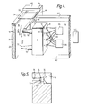
- Figure 4 this shows the construction illustrated in Figure 1 in more detail.
- Figure 5 is a sectional view of block 6.
- Each PCB 4 is mounted in top and bottom slide rails 40, 42 for permitting the PCB to be slide in and out easily from rack 2.
- the slide rails 40, 42 are secured at the rear end of rack 2 to an orthogonal framework 44 which provides reference surfaces 46.
- framework 44 has extension portions 48 for securing a rectangular frame member 50 which secures block 20 in position.
- Each PCB 4 has at its front end pusher members 52 for pushing the circuit card into the rack and for manoeuvring the circuit card, as will be explained below.
- the rear end of the circuit card carries alimi- nium rectangular block 6 which is screwed to the circuit board and which contains rows of through holes 56, which house photo detectors 10 and laser transmitters 8 respectively. These detectors and laser transmitters are coupled via short electrical leads 62 to MUX/DEMUX chips 64.
- leads 62 may be replaced by optical fibres, and the laser sources and photo detectors may be mounted on the circuit board.
- the rear end of block 6 carries two tapering conical spike members 70 which engage in registering apertures 72 in block 20.
- Pusher members 52 are held manually when circuit board 4 is inserted into rails 40, 42 and the board is manoeuvered so that block 54 comes to rest against reference surfaces 46 while projecting members 70 engage in aperture 72.
- laser diode 70 emits visible light which is collimated using a single piano-convex lens 72.
- the focal length of the lens was 1.47mm with a 30 distribution of less than 1%. Since the variation between the focal length of the lenses is small it is possible to avoid the need for an individual focusing arrangement for each lens.
- a shoulder 74 within the hole in the heat sink block is used to provide the alignment of the lens position. Since the normal operating power for the laser is 3 times the eye safe limit it is possible to use a restricted aperture 76 to reduce the astigmatism in the laser output.
- the aperture 76 was arranged to clip the large angle axis before the lens thus providing a more circular symmetric output beam but still at the required level of ⁇ 1 mW.
- the holograms 18 on a on a photographic plate are mounted to a solid polymer block 20 using an optically curing epoxy resin.
- the fast curing allowed the hologram to be aligned then bonded into position.
- the advantages of the solid structure are that it will remain aligned during use and it also prevents dust and other unwanted particles from blocking the beam.
- a polymethyl methacrylate (PMMA) polymer was used since it has good mechanical properties and has a minimum loss near the 670nm operating wavelength.
- the path length of each beam varies as a function of projected angle, between 300mm and 470mm.
- the block 20 is precision cut such that the front and back faces were parallel and perpendicular to the other faces. Then a final polish was applied to the two faces. Precision cutting and polishing processes are used to minimise the amount of stress induced in the blocks.
- reflective surface 22 is applied directly to the back surface of the block.
- the reflector is created using a high vacuum aluminium evaporation process. Since the back face has been cut and polished perpendicular no further alignment of the reflector is necessary. The reflection at the surface was measured at HeNe as 75.6%.
- the surace is cleaned rigorously before aluminiumisation so that a good adhesion to the polymer is achieved. However, a protective film or lamination is required to prevent damage from abrasion or chemical attack.
- the holograms for the backplane were fabricated using Agfa 8E75HD silver halide holographic plates.
- the output from a HeNe laser (633nm wavelength) was split into two collimated plane waves.
- the two beams were incident onto the holographic plate from the same side of the plate such that interference fringes were constructed in the photographic material ( Figure 3).
- the bright fringes exposes the silver halide releasing free silver atoms.
- Developing the plates fixes the interference fringes as a variation in the absorbtion of the photographic emulsion.
- a bleaching process is then used to convert the silver atoms back into stable silver halide thus giving the required refractive index variation.
- the holograms were recorded using beams from the same side of the plate when the hologram is replayed with a beam transmitted through the hologram the beam is steered through an angle 0.
- the angle 0 is the angle at which the reference beam illumuniates the plate in air.
- the holograms are bonded to a polymer block and a correction for the refraction at the hologram/polymer interface has to be made using Snell's law.
- the percentage of power in the desired first order beam varies with the steering angle required.
- a range of angles from 35° to 70° were tested. The range of angles available is limited by the thickness of the holographic emulsion and maximum spatial frequency achievable in the emulsion. In the plates used the emulsion thickness is ⁇ 5 f..lm, at this thickness the plates behave partly as a thick hologram and partly as a thin hologram. Thus if both the reference and object recording beams are approximately normal to the plate surface (low steering angles) the emulsion thickness 'seen' by the light is small and the hologram behaves as a thin grating.
- Each of the Holographic Optical Elements is characterised at the HeNe 633nm wavelength.
- the percentage power in the zero and first order, (straight through and the required steered beam) is measured. From this, the conversion efficiency, the ratio of power in the first order as a percentage of the input power, is calculated. The highest efficiencies are obtained in the middle of the angle range and declined at larger angles. The average conversion efficiency at 35.06° is 40% or 4dB.
Abstract
Description
- This invention relates to a system for interconnection of a stack of circuit broads, and relates particularly though not exclusively to circuit cards used in telecommunications switches or computers.
- In the field of telecommunications switches, with increased circuit density and higher switch speed rates (200 Mbits-1 increasing to 2.4 Gbits-1 in the future), many proposals have been made for more efficient interconnections of the circuit boards comprising the switch. One area of critical importance is the backplane or motherboard which provides interconnections between the circuit boards. In addition to considerations such as removing heat generated during operation, one important consideration is distribution of clock signals etc to the various boards; at such high bit rates, the problems of propagation delay, bandwidth and crosstalk arise by the clock signals being conducted along conductors in the backplane.
- It is known, see K.H. Brenner and F. Sauer "Diffractive-Reflective Optical Interconnects" Applied Optics 15th October 1988, Vol 27, No. 20 to employ hologram elements disposed on a surface to reflect or refract light between transmitters and receivers on an adjacent substrate. Usually the transmitters and receivers form part of an array of integrated circuit chips and the light is employed to distribute signals to the various chips with increased efficiency. The surface carrying the holograms is normally bonded to the chip substrate via a transparent medium to form a compact and monolithic assembly: this is required because of the high accuracy required in alignment of the various optical paths.
- It is an object of the present invention to provide a system for interconnection of a stack of circuit boards which overcomes the problems outlined above.
- The present invention provides a system for interconnection of a stack of circuit boards, wherein each of at least a plurality of the circuit boards has an end region carrying one or more light transmitters or light receivers, an optical structure forming an interconnecting backplane for the circuit boards, the optical structure comprising a first surface carrying a multiplicity of hologram elements disposed to receive light from said light transmitters and to route such light to a second reflective surface where the light is reflected back to said hologram elements for routing to said light receivers.
- Thus in accordance with the invention, by providing an optical structure which provides an interconnecting backplane for the circuit boards, the problems of known backplanes are overcome, in particular the problems with very high signal bit rates.
- A further advantage of an optical interconnection scheme is a reduction of the insertion force and the alignment requirements of the connectors. An optical connector requires only the force to mate an alignment shell and a few electrical services such as power and clock. By contrast the electrical connector has to reliably mate a large number of pins requiring a large insertion force. This force together with the long thin board design introduces considerable problems relating to flexing and bowing of the cards and connectors.
- Further a trade-off can be made between the optical power budget and the alignment requirements. By expanding the laser beam the lateral tolerance can be considerably relaxed at the expense of an accompanying power budget penalty. However, since laser sources (whose maximum power is limited only by safety considerations) are used and the transmission distances are short a considerable design margin in the power budget exists. This makes it possible to make allowance for bow in the boards, slight misalignment of connectors, or connectors not fully engaging.
- As regards environmental stability of the optical structure, free space optical interconnection techniques are susceptible to particles obscuring the beam. These can either be transient effects such as an air borne particle moving through the beam causing momentary dropout of the signal or more permanent effects such as particles becoming adhered to the surface of mirrors or lenses. The optical structure may use a solid glass or plastic structures for the majority of the beam propagation paths. In addition to confining the beam and thus preventing problems with dust this has the added advantage of giving the optical structure mechanical stability thus reducing alignment problems. The use of plastics also allow the parts to be cast or moulded at low costs. The disadvantage of using a solid medium for the optical interconnect region is, however, the reduction of ventilation routes along the back of a rack. Alternatively and as preferred free space is employed as the optical medium and a flexible (rubber) sealing surround is provided between the circuit cards and the optical backplane to prevent the ingress of dust.
- Careful mechanical design of the system is required at two main stages. First, the initial system must be straight forward to align during manufacture. Second, the system must remain aligned during shipping and use. This is particularly important for the holographic system where the sensitivity to alignment is greatest.
- A further consideration with holographic techniques relates to the temperature and the humidity range experienced by the components both during shipping and operation. Some of the high efficiency materials used for the fabrication of the holographic optical elements such as dichromated gelatin (DCG) have a high sensitivity to humidity requiring coatings to protect them.
- To this end, said first surface on which the hologram elements are mounted is formed by a transparent sheet which either carries said second reflective surface, or is bonded to another transparent sheet carrying said second reflective surface, to form a monolithic structure. Such structure is mounted securely to a framework for housing the printed circuit boards. A metal block is secured to the end of each printed circuit board adjacent the backplane and carries the transmitter and receiver optical elements which are mounted in holes accurately positioned in the metal block. The framework for the PCB stack carries reference surfaces adjacent the backplane and as each PCB is positioned into the framework, the metal block abuts the reference surfaces to accurately space the block from the holograms. In addition in accordance with a further preferred feature of the invention the metal block carries one or more projecting and tapering members, for example a spike, for registering in holes in the first surface for alignment of the optics. Alternatively the first surface may carry projecting members for registering in apertures in this block. In any event the circuit board is provided with "pusher" members for guiding and manoeuvring the board into its registering and aligned position.
- At the very high bit rates employed it will be important to minimise the distances of the electrical interface between optical transmitter and receiver and MUX/DEMUX chips respectively. For ease of construction it may then be preferable to use an optical fibre 'light pipe' to route the optical signal to a more convenient position on the printed circuit board.
- A preferred embodiment of the invention will now be described with reference to the accompanying drawings, wherein:
- Figure 1 is a schematic view of the layout of an optical backplane in accordance with the invention interconnecting a stack of circuit cards;
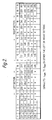
- Figure 2 is an interconnection pattern for the backplane of Figure 1;
- Figure 3 are schematic views of the manneroffor- mation of a hologram;
- Figures 4 is a more detailed view of the mechanical construction of the backplane; and
- Figure 5 is a sectional view of the block of Figure 4 secured to a circuit card carrying the optical transmitters and receivers.
- Referring now to Figure 1, a
rack 2 provides a framework for housing a stack of printedcircuit cards 4. Each card has at its rear end ablock 6 housing a plurality oftransmitters 8 andreceivers 10. Anoptical backplane 12 is rigidly mounted torack 2 byframework members 14 and comprises asurface 16 carrying a plurality ofhologram elements 18. Thesurface 16 is provided by a silver halide holographic plate which is aligned and bonded to an optically transparent solidpolymeric block 20. Aback reflector 22 is deposited directly on the back ofpolymeric plate 20. - The holograms are so arranged in relation to the
transmitters 8 andreceivers 10 that light from a transmitter is refracted by a first hologram into a predetermined direction, reflected fromreflective plate 22 to another hologram element, whence it is against refracted to a desired receiver orphoto detector 10. This is indicated schematically in Figure 1. The holographic elements are arranged such that a collimated beam entering a first hologram perpendicular to the first surface emerges perpendicular at the desired output point. Aflexible rubber cover 24 is positioned around the free space betweenrack 2 and the optical backplate in order to prevent the ingress of dirt which might interfere with the laser beams. - Referring now to Figure 4 this shows the construction illustrated in Figure 1 in more detail. In addition, Figure 5 is a sectional view of
block 6. - Each
PCB 4 is mounted in top andbottom slide rails rack 2. Theslide rails rack 2 to anorthogonal framework 44 which providesreference surfaces 46. Inaddition framework 44 hasextension portions 48 for securing arectangular frame member 50 which securesblock 20 in position. - Each
PCB 4 has at its frontend pusher members 52 for pushing the circuit card into the rack and for manoeuvring the circuit card, as will be explained below. The rear end of the circuit card carries alimi- niumrectangular block 6 which is screwed to the circuit board and which contains rows of throughholes 56, whichhouse photo detectors 10 andlaser transmitters 8 respectively. These detectors and laser transmitters are coupled via shortelectrical leads 62 to MUX/DEMUX chips 64. As an alternative construction leads 62 may be replaced by optical fibres, and the laser sources and photo detectors may be mounted on the circuit board. - The rear end of
block 6 carries two taperingconical spike members 70 which engage in registeringapertures 72 inblock 20.Pusher members 52 are held manually whencircuit board 4 is inserted intorails members 70 engage inaperture 72. - Referring to Figure 5 which shows the optics associated with a
laser transmitter 8,laser diode 70 emits visible light which is collimated using a single piano-convex lens 72. The focal length of the lens was 1.47mm with a 30 distribution of less than 1%. Since the variation between the focal length of the lenses is small it is possible to avoid the need for an individual focusing arrangement for each lens. Ashoulder 74 within the hole in the heat sink block is used to provide the alignment of the lens position. Since the normal operating power for the laser is 3 times the eye safe limit it is possible to use a restrictedaperture 76 to reduce the astigmatism in the laser output. Theaperture 76 was arranged to clip the large angle axis before the lens thus providing a more circular symmetric output beam but still at the required level of ≈ 1 mW. - The
holograms 18 on a on a photographic plate are mounted to asolid polymer block 20 using an optically curing epoxy resin. The fast curing allowed the hologram to be aligned then bonded into position. The advantages of the solid structure are that it will remain aligned during use and it also prevents dust and other unwanted particles from blocking the beam. A polymethyl methacrylate (PMMA) polymer was used since it has good mechanical properties and has a minimum loss near the 670nm operating wavelength. The path length of each beam varies as a function of projected angle, between 300mm and 470mm. - The
block 20 is precision cut such that the front and back faces were parallel and perpendicular to the other faces. Then a final polish was applied to the two faces. Precision cutting and polishing processes are used to minimise the amount of stress induced in the blocks. - After polishing
reflective surface 22 is applied directly to the back surface of the block. The reflector is created using a high vacuum aluminium evaporation process. Since the back face has been cut and polished perpendicular no further alignment of the reflector is necessary. The reflection at the surface was measured at HeNe as 75.6%. The surace is cleaned rigorously before aluminiumisation so that a good adhesion to the polymer is achieved. However, a protective film or lamination is required to prevent damage from abrasion or chemical attack. - The holograms for the backplane were fabricated using Agfa 8E75HD silver halide holographic plates. The output from a HeNe laser (633nm wavelength) was split into two collimated plane waves. The two beams were incident onto the holographic plate from the same side of the plate such that interference fringes were constructed in the photographic material (Figure 3). The bright fringes exposes the silver halide releasing free silver atoms. Developing the plates then fixes the interference fringes as a variation in the absorbtion of the photographic emulsion. A bleaching process is then used to convert the silver atoms back into stable silver halide thus giving the required refractive index variation. Since the holograms were recorded using beams from the same side of the plate when the hologram is replayed with a beam transmitted through the hologram the beam is steered through an
angle 0. As the object beam was normal to the plate theangle 0 is the angle at which the reference beam illumuniates the plate in air. The holograms are bonded to a polymer block and a correction for the refraction at the hologram/polymer interface has to be made using Snell's law. - The percentage of power in the desired first order beam varies with the steering angle required. For the type of holographic media used a range of angles from 35° to 70° were tested. The range of angles available is limited by the thickness of the holographic emulsion and maximum spatial frequency achievable in the emulsion. In the plates used the emulsion thickness is ≈ 5 f..lm, at this thickness the plates behave partly as a thick hologram and partly as a thin hologram. Thus if both the reference and object recording beams are approximately normal to the plate surface (low steering angles) the emulsion thickness 'seen' by the light is small and the hologram behaves as a thin grating. In such a case multiple orders are generated resulting in a large number of unwanted beams and a reduction in the power in the output beam. At high deflection angles the spatial frequency required in the holographic material increases. Since there is a finite grain size for the silver halide plates this sets the maximum angle through which the beam can be deviated.
- Using an alternative thicker volume hologram material such as dichromated gelatine or a photo-polymer will extend the range of angles achievable. Although this will increase the range of angles achievable other factors will limit the eventual performance.
- Each of the Holographic Optical Elements is characterised at the HeNe 633nm wavelength. The percentage power in the zero and first order, (straight through and the required steered beam) is measured. From this, the conversion efficiency, the ratio of power in the first order as a percentage of the input power, is calculated. The highest efficiencies are obtained in the middle of the angle range and declined at larger angles. The average conversion efficiency at 35.06° is 40% or 4dB.
Claims (13)
Applications Claiming Priority (2)
| Application Number | Priority Date | Filing Date | Title |
|---|---|---|---|
| GB909024713A GB9024713D0 (en) | 1990-11-14 | 1990-11-14 | Optical backplane interconnecting circuit boards |
| GB9024713 | 1990-11-14 |
Publications (2)
| Publication Number | Publication Date |
|---|---|
| EP0486208A2 true EP0486208A2 (en) | 1992-05-20 |
| EP0486208A3 EP0486208A3 (en) | 1993-03-31 |
Family
ID=10685334
Family Applications (1)
| Application Number | Title | Priority Date | Filing Date |
|---|---|---|---|
| EP19910310258 Withdrawn EP0486208A3 (en) | 1990-11-14 | 1991-11-06 | Optical backplane interconnecting circuit boards |
Country Status (11)
| Country | Link |
|---|---|
| US (1) | US5182780A (en) |
| EP (1) | EP0486208A3 (en) |
| JP (1) | JPH04286191A (en) |
| KR (1) | KR920010320A (en) |
| CN (1) | CN1063172A (en) |
| AU (1) | AU8787491A (en) |
| CA (1) | CA2055301A1 (en) |
| FI (1) | FI915357A (en) |
| GB (2) | GB9024713D0 (en) |
| IE (1) | IE913878A1 (en) |
| PT (1) | PT99510A (en) |
Cited By (11)
| Publication number | Priority date | Publication date | Assignee | Title |
|---|---|---|---|---|
| WO1994018587A1 (en) * | 1993-02-05 | 1994-08-18 | Gec-Marconi Limited | Optical backplanes |
| WO1996000919A1 (en) * | 1994-06-30 | 1996-01-11 | The Whitaker Corporation | Passively aligned bi-directional optoelectronic transceiver module assembly |
| FR2723644A1 (en) * | 1994-08-09 | 1996-02-16 | Matra Defense | Digital optical interconnector providing connection between parallel printed circuit boards |
| WO1996010201A1 (en) * | 1994-09-28 | 1996-04-04 | Siemens Aktiengesellschaft | Subrack for plug-in electric modules |
| WO1996010763A1 (en) * | 1994-09-30 | 1996-04-11 | Siemens Aktiengesellschaft | Device for interconnecting electronic apparatuses and allowing them to communicate with each other |
| WO2001050170A2 (en) * | 1999-12-29 | 2001-07-12 | Corning Incorporated | Optical communication system with pluggable wdm-module |
| US6751014B2 (en) | 2001-06-19 | 2004-06-15 | International Business Machines Corporation | Automatic gain control and dynamic equalization of erbium doped optical amplifiers in wavelength multiplexing networks |
| US6970649B2 (en) | 2001-10-30 | 2005-11-29 | International Business Machines Corporation | WDMA free space broadcast technique for optical backplanes and interplanar communications |
| US7062166B2 (en) | 2001-09-26 | 2006-06-13 | International Business Machines Corporation | First and second derivative processing of wavelength multiplexed optical signals |
| US7061944B2 (en) | 2001-05-25 | 2006-06-13 | International Business Machines Corporation | Apparatus and method for wavelength-locked loops for systems and applications employing electromagnetic signals |
| WO2012130691A1 (en) * | 2011-03-30 | 2012-10-04 | Fujitsu Technology Solutions Intellectual Property Gmbh | Rack, server and assembly comprising such a rack and at least one server |
Families Citing this family (18)
| Publication number | Priority date | Publication date | Assignee | Title |
|---|---|---|---|---|
| CA2084950A1 (en) * | 1991-12-18 | 1993-06-19 | Tsen-Hwang Lin | Compact programmable processing module |
| EP0548440A1 (en) * | 1991-12-23 | 1993-06-30 | International Business Machines Corporation | Bilithic composite for optoelectronic integration |
| US5412506A (en) * | 1992-03-09 | 1995-05-02 | At&T Corp. | Free-space optical interconnection arrangement |
| JP3326959B2 (en) * | 1994-04-25 | 2002-09-24 | 松下電器産業株式会社 | Optical fiber module |
| GB2299459B (en) * | 1995-03-29 | 1998-09-30 | Northern Telecom Ltd | Equipment practice |
| GB2311381A (en) * | 1996-03-22 | 1997-09-24 | Northern Telecom Ltd | Equipment modules and backplane with optical connection |
| DE19618149B4 (en) * | 1996-05-07 | 2005-01-20 | Daimlerchrysler Ag | Optical connection strip |
| DE69730378T2 (en) * | 1996-06-03 | 2005-08-18 | Nippon Telegraph And Telephone Corp. | Optical system to plate to plate and unit-to-unit bonding |
| US5832147A (en) * | 1996-11-27 | 1998-11-03 | Motorola, Inc. | Holographic optical interconnect system and method for board-to-board and chip-to-chip communication interconnections |
| US6125417A (en) | 1997-11-14 | 2000-09-26 | International Business Machines Corporation | Hot plug of adapters using optical switches |
| US5978526A (en) * | 1997-12-19 | 1999-11-02 | Motorola, Inc. | Method, multi-channel optical interconnect device, and a multi-channel optically interconnected electronic device for minimizing cross-talk between a plurality of optical signals |
| DE19823587A1 (en) * | 1998-05-27 | 1999-12-02 | Alcatel Sa | Optical connection and connection unit for exchanging data between devices |
| US6583902B1 (en) | 1999-12-09 | 2003-06-24 | Alvesta, Inc. | Modular fiber-optic transceiver |
| US6549027B1 (en) | 2000-02-01 | 2003-04-15 | Sun Microsystems, Inc. | Apparatus and method for testing for compatibility between circuit boards |
| US6823100B1 (en) * | 2001-08-27 | 2004-11-23 | Incucomm, Inc. | Optical backplane for use with a communications equipment chassis and method of operation therefor |
| US7416352B2 (en) * | 2005-09-08 | 2008-08-26 | Northrop Grumman Corporation | Optical multi-channel free space interconnect |
| US7277611B1 (en) * | 2006-08-30 | 2007-10-02 | Fujitsu, Limited | Optical interconnect platform including Bragg diffractive gratings in a bulk material |
| US8452137B2 (en) | 2011-01-10 | 2013-05-28 | Avago Technologies General Ip (Singapore) Pte. Ltd. | Optical backplane having at least one optical relay element for relaying light from an input facet of the backplane to an output facet of the backplane |
Citations (3)
| Publication number | Priority date | Publication date | Assignee | Title |
|---|---|---|---|---|
| WO1985003179A1 (en) * | 1984-01-09 | 1985-07-18 | Hase Klaus Ruediger | Circuit with optical bus |
| EP0268404A2 (en) * | 1986-11-14 | 1988-05-25 | AT&T Corp. | Optical interconnection of devices on chips |
| US4946253A (en) * | 1989-10-16 | 1990-08-07 | Arizona Board Of Regents For And On Behalf Of The University Of Arizona | Reconfigurable substrate-mode holographic interconnect apparatus and method |
Family Cites Families (9)
| Publication number | Priority date | Publication date | Assignee | Title |
|---|---|---|---|---|
| US4671603A (en) * | 1983-11-17 | 1987-06-09 | Pilkington P.E. Limited | Optical filters and multiplexing-demultiplexing devices using the same |
| FR2590995B1 (en) * | 1985-02-26 | 1988-08-19 | Thomson Csf | DEVICE FOR OPTICALLY INTERCONNECTING ELECTRONIC COMPONENT BOARDS IN A BOX AND MANUFACTURING METHOD |
| US4807955A (en) * | 1987-08-06 | 1989-02-28 | Amp Incorporated | Opto-electrical connecting means |
| US4838630A (en) * | 1987-12-21 | 1989-06-13 | Physical Optics Corporation | Holographic planar optical interconnect |
| EP0335104A3 (en) * | 1988-03-31 | 1991-11-06 | Siemens Aktiengesellschaft | Arrangement to optically couple one or a plurality of optical senders to one or a plurality of optical receivers of one or a plurality of integrated circuits |
| EP1187227A3 (en) * | 1989-05-31 | 2002-08-28 | Osram Opto Semiconductors GmbH & Co. OHG | Surface-mountable optical element and method of fabrication |
| US5073000A (en) * | 1990-05-21 | 1991-12-17 | Motorola, Inc. | Optical interconnect printed circuit structure |
| US5101465A (en) * | 1990-08-07 | 1992-03-31 | At&T Bell Laboratories | Leadframe-based optical assembly |
| US5061027A (en) * | 1990-09-04 | 1991-10-29 | Motorola, Inc. | Solder-bump attached optical interconnect structure utilizing holographic elements and method of making same |
-
1990
- 1990-11-14 GB GB909024713A patent/GB9024713D0/en active Pending
-
1991
- 1991-11-06 EP EP19910310258 patent/EP0486208A3/en not_active Withdrawn
- 1991-11-06 IE IE387891A patent/IE913878A1/en not_active Application Discontinuation
- 1991-11-06 GB GB9123577A patent/GB2253317B/en not_active Expired - Fee Related
- 1991-11-12 CA CA002055301A patent/CA2055301A1/en not_active Abandoned
- 1991-11-13 US US07/791,458 patent/US5182780A/en not_active Expired - Fee Related
- 1991-11-13 FI FI915357A patent/FI915357A/en not_active Application Discontinuation
- 1991-11-14 JP JP3326422A patent/JPH04286191A/en active Pending
- 1991-11-14 KR KR1019910020257A patent/KR920010320A/en not_active Application Discontinuation
- 1991-11-14 AU AU87874/91A patent/AU8787491A/en not_active Abandoned
- 1991-11-14 CN CN91111548A patent/CN1063172A/en active Pending
- 1991-11-14 PT PT99510A patent/PT99510A/en not_active Application Discontinuation
Patent Citations (3)
| Publication number | Priority date | Publication date | Assignee | Title |
|---|---|---|---|---|
| WO1985003179A1 (en) * | 1984-01-09 | 1985-07-18 | Hase Klaus Ruediger | Circuit with optical bus |
| EP0268404A2 (en) * | 1986-11-14 | 1988-05-25 | AT&T Corp. | Optical interconnection of devices on chips |
| US4946253A (en) * | 1989-10-16 | 1990-08-07 | Arizona Board Of Regents For And On Behalf Of The University Of Arizona | Reconfigurable substrate-mode holographic interconnect apparatus and method |
Non-Patent Citations (1)
| Title |
|---|
| APPLIED OPTICS vol. 27, no. 20, 15 October 1988, pages 4251 - 4254 BRENNER, SAUER 'Diffractive-reflective optical interconnects.' * |
Cited By (16)
| Publication number | Priority date | Publication date | Assignee | Title |
|---|---|---|---|---|
| WO1994018587A1 (en) * | 1993-02-05 | 1994-08-18 | Gec-Marconi Limited | Optical backplanes |
| WO1994018589A1 (en) * | 1993-02-05 | 1994-08-18 | Gec-Marconi Limited | Optical backplanes |
| WO1994018588A1 (en) * | 1993-02-05 | 1994-08-18 | Gec-Marconi Limited | Optical backplanes |
| WO1996000919A1 (en) * | 1994-06-30 | 1996-01-11 | The Whitaker Corporation | Passively aligned bi-directional optoelectronic transceiver module assembly |
| FR2723644A1 (en) * | 1994-08-09 | 1996-02-16 | Matra Defense | Digital optical interconnector providing connection between parallel printed circuit boards |
| WO1996010201A1 (en) * | 1994-09-28 | 1996-04-04 | Siemens Aktiengesellschaft | Subrack for plug-in electric modules |
| WO1996010763A1 (en) * | 1994-09-30 | 1996-04-11 | Siemens Aktiengesellschaft | Device for interconnecting electronic apparatuses and allowing them to communicate with each other |
| US5923451A (en) * | 1994-09-30 | 1999-07-13 | Siemens Aktiengesellschaft | Means for connecting electronic devices for communication with one another |
| WO2001050170A2 (en) * | 1999-12-29 | 2001-07-12 | Corning Incorporated | Optical communication system with pluggable wdm-module |
| WO2001050170A3 (en) * | 1999-12-29 | 2002-02-14 | Corning Inc | Optical communication system with pluggable wdm-module |
| US7061944B2 (en) | 2001-05-25 | 2006-06-13 | International Business Machines Corporation | Apparatus and method for wavelength-locked loops for systems and applications employing electromagnetic signals |
| US6751014B2 (en) | 2001-06-19 | 2004-06-15 | International Business Machines Corporation | Automatic gain control and dynamic equalization of erbium doped optical amplifiers in wavelength multiplexing networks |
| US7062166B2 (en) | 2001-09-26 | 2006-06-13 | International Business Machines Corporation | First and second derivative processing of wavelength multiplexed optical signals |
| US6970649B2 (en) | 2001-10-30 | 2005-11-29 | International Business Machines Corporation | WDMA free space broadcast technique for optical backplanes and interplanar communications |
| WO2012130691A1 (en) * | 2011-03-30 | 2012-10-04 | Fujitsu Technology Solutions Intellectual Property Gmbh | Rack, server and assembly comprising such a rack and at least one server |
| US9582450B2 (en) | 2011-03-30 | 2017-02-28 | Fujitsu Technology Solutions Intellectual Property Gmbh | Rack, server and assembly comprising such a rack and at least one server |
Also Published As
| Publication number | Publication date |
|---|---|
| IE913878A1 (en) | 1992-05-20 |
| GB9024713D0 (en) | 1991-01-02 |
| GB9123577D0 (en) | 1992-01-02 |
| CA2055301A1 (en) | 1992-05-15 |
| JPH04286191A (en) | 1992-10-12 |
| GB2253317A (en) | 1992-09-02 |
| AU8787491A (en) | 1992-05-21 |
| KR920010320A (en) | 1992-06-26 |
| EP0486208A3 (en) | 1993-03-31 |
| US5182780A (en) | 1993-01-26 |
| GB2253317B (en) | 1994-10-19 |
| FI915357A (en) | 1992-05-15 |
| FI915357A0 (en) | 1991-11-13 |
| PT99510A (en) | 1993-12-31 |
| CN1063172A (en) | 1992-07-29 |
Similar Documents
| Publication | Publication Date | Title |
|---|---|---|
| US5182780A (en) | Optical backplane interconnecting circuit boards | |
| EP0322218B1 (en) | Holographic planar optical interconnect | |
| US5202567A (en) | Optical information transmitting device and method of manufacturing same | |
| US5500523A (en) | Optical information transmitting device and method of manufacturing same | |
| US5204866A (en) | Bidirectional free-space optical bus for electronics systems | |
| US5113403A (en) | Bidirectional free-space optical bus for electronics systems | |
| JPH06259800A (en) | Optical device | |
| WO1998023981A1 (en) | Holographic optical interconnect system and method | |
| Haumann et al. | Optoelectronic interconnection based on a light-guiding plate with holographic coupling elements | |
| US5987198A (en) | Optical bus and optical bus production method including a plurality of light transmission paths | |
| US6172783B1 (en) | Optical bus and signal processor | |
| US5515462A (en) | Optical interconnect in optical packages using holograms | |
| CN109116469A (en) | Optical module | |
| US6498875B1 (en) | Optical connector for connecting a plurality of light sources to a plurality of light sinks | |
| US10782480B2 (en) | Integrated optoelectronic chip and lens array | |
| JP2576473B2 (en) | Optical wiring circuit unit | |
| Kawai et al. | Two-dimensional optical buses for massively parallel processing | |
| Kim et al. | Optical interconnects for multiprocessors in computer backplane | |
| Kostuk et al. | Multiprocessor optical bus | |
| Plawsky et al. | Photochemically machined, glass ceramic, optical fiber interconnection components | |
| JPH11183757A (en) | Optical bus system and signal processor | |
| GB2487105A (en) | An optical backplane for propagating a light beam | |
| JPS59149069A (en) | Light-receiving element for optical communication | |
| HAMANAKA et al. | OPTICAL BUS INTERCONNECTION SYSTEM (OBIS) | |
| Mukherjee | Opto-Electronic Multi-Chip Modules (OE-MCMs): Current R&D and Applications to Microelectronic Interconnections |
Legal Events
| Date | Code | Title | Description |
|---|---|---|---|
| PUAI | Public reference made under article 153(3) epc to a published international application that has entered the european phase |
Free format text: ORIGINAL CODE: 0009012 |
|
| AK | Designated contracting states |
Kind code of ref document: A2 Designated state(s): BE DE DK ES FR GR IT LU NL SE |
|
| PUAL | Search report despatched |
Free format text: ORIGINAL CODE: 0009013 |
|
| AK | Designated contracting states |
Kind code of ref document: A3 Designated state(s): BE DE DK ES FR GR IT LU NL SE |
|
| 17P | Request for examination filed |
Effective date: 19930908 |
|
| 17Q | First examination report despatched |
Effective date: 19950316 |
|
| STAA | Information on the status of an ep patent application or granted ep patent |
Free format text: STATUS: THE APPLICATION IS DEEMED TO BE WITHDRAWN |
|
| 18D | Application deemed to be withdrawn |
Effective date: 19950727 |